A silicon spin vacuum: isotopically enriched 28silicon-on-insulator and 28silicon from ultra-high fluence ion implantation
Abstract
Isotopically enriched silicon (Si) can greatly enhance qubit coherence times by minimizing naturally occurring 29Si which has a non-zero nuclear spin. Ultra-high fluence 28Si ion implantation of bulk natural Si substrates was recently demonstrated as an attractive technique to ultra-high 28Si isotopic purity. In this work, we apply this 28Si enrichment process to produce 28Si and 28Si-on-insulator (SOI) samples. Experimentally, we produced a 28Si sample on natural Si substrate with 29Si depleted to 7 ppm (limited by measurement noise floor), that is at least 100 nm thick. This is achieved with an ion energy that results in a sputter yield of less than one and a high ion fluence, as supported by simulations. Further, our simulations predict the 29Si and 30Si depletion in our sample to be less than 1 ppm. In the case of SOI, ion implantation conditions are found to be more stringent than those of bulk natural Si in terms of minimizing threading dislocations upon subsequent solid phase epitaxy annealing. Finally, we report the observation of nanoscopic voids in our 28SOI and 28Si samples located in the depth region between the surface and 70 nm. These voids appear to be stabilized by the presence of gold impurities and can be annealed out completely by a standard SPE annealing protocol at 620∘C for 10 minutes in the absence of gold.
I Introduction
Ultra-high fluence 28Si self-implantation ( cm-2) can be used as a means to isotopically enrich natural silicon (natSi) substrates to unprecedented purity levels. [1, 2] With the fast growing interest in quantum technology research, 28Si substrates are important to Si-based quantum information processing (QIP) platforms such as gate-defined quantum dot qubits, [3, 4, 5] flip-flop donor qubits, [6, 7, 8] and Er-doped Si quantum emitters [9, 10] due to the zero nuclear spin of 28Si isotopes and weak spin-orbit coupling in Si. natSi consists of 4.7 at.% of the non-zero nuclear spin isotope 29Si , leading to decoherence of qubits by spectral diffusion. [11] The other stable isotope, 30Si, present to 3.1 at.% has and does not contribute to decoherence via magnetic interactions, however, it can introduce higher order perturbations to the Hamiltonian via strain interactions. [12] An ideal substrate would therefore consist of isotopically pure monocrystalline 28Si, the much sought-after ‘semiconductor spin vacuum’. [13]
The ultra-high fluence 28Si self-implantation process, which we refer to as the ‘28Si enrichment process’, presents itself as a cost-effective and competitive alternative to existing 28SiF4-based growth techniques [14, 15, 16, 17, 18, 19, 20] and molecular beam epitaxy (MBE). [21] 28SiF4-based techniques rely on toxic and expensive isotopically pure 28SiF4 gas as its source material. The resultant Si purity is limited by that of the source and can result in purities as low as 50 ppm 29Si. This material has been used in the Avogadro project to define the kilogram. [22] A similar level of isotopic purity can also be achieved through solid source MBE (50 ppm 29Si) which uses 28Si wafers as its source material. [21] In contrast, the 28Si enrichment process employed in the present work uses natSi as both its source and starting materials. A natSi ion beam is accelerated through a standard magnetic field-based charge-to-mass analyzer and the 28Si ion beam is mass selected. Through the continuous bombardment of this 28Si ion beam into a natSi substrate, 29Si and 30Si are gradually sputtered away, resulting in isotopically purified 28Si surface layers with a thickness of nm. [1] The ion bombardment results in a transformation to the amorphous silicon phase and a subsequent moderate to high temperature anneal leads to solid phase epitaxial (SPE) regrowth of single crystal silicon with negligible diffusion of the implanted atoms expected. [23, 24, 25] A four to five-fold improvement in the 31P donor electron spin coherence time as compared to natSi has been achieved with a 0.3 at.% 29Si (3000 ppm) sample produced by 28Si enrichment. [1] Indeed, the donor coherence time measured in Ref. 26 was limited by inter-donor coupling/instantaneous diffusion, thus leading one to expect even longer qubit coherence times in these isotopically enriched 28Si samples. [25]
Recently, a 29Si depletion of 2.3 ppm has been achieved using the 28Si enrichment process simply by increasing the ion implantation fluence to cm-2.[2] This will presumably yield an improved semiconductor vacuum and surpass depletion levels attainable with the 28SiF4-based technique. To achieve such a high purity with the 28Si enrichment process, a high ion beam flux and fluence are typically required. Previous work in Refs. 1 and 2 employed a flux of /cm2 and /cm2, respectively, and fluences between to . However, it is unclear whether the use of high ion fluxes and fluences will negate the benefits of isotopic purity via the formation of microstructural defects as a result of increased damage production rates, localized beam heating, and dynamic annealing during ion implantation. [27, 28, 29, 30, 26]
Furthermore, it is well-known from both simulations and experiments that there is a spatial separation between the vacancy and interstitial distributions generated by the ion collisions during implantation. [31, 32] An excess of vacancies is expected near the surface up to approximately half the ion projected range () while an excess of interstitials is expected deeper in the substrate up to around one to two times the ion projected range (1 to ). For Si implanted under non-amorphizing conditions, this spatial separation results in the formation of open volume defects (vacancy clusters, voids) and interstitial clusters (loops, rods, dislocations) in these depth ranges, respectively. [33, 34, 35, 36, 37] These defects have been observed experimentally and are stable up to temperatures of 850 to 900∘C. For Si implanted under amorphizing conditions, to our knowledge, there is no experimental evidence for the presence of similar complex defect clusters. [29, 38, 39, 40] Nevertheless, we expect the same spatial separation of vacancies and interstitials in Si following amorphizing ion implantation, especially in high fluence implantation such as that considered in this work. The interplay between point defect generation (determined by the ion flux), clustering (determined by the ion flux and sample temperature) and annihilation (influenced by the sample temperature) rates will therefore dictate whether open volumes can form and stabilize near the sample surface. [28] Further, these open volumes (if present) will be in close proximity to qubits (usually located within 20 nm of the surface) and thus it is important to investigate the possibility of their formation and thermal stability under further processing, as explored in this work.
In this work, we investigate the 28Si enrichment process using a range of ion beam flux and fluence values. We also consider the impact of ion implantation energy and sample temperature on both the 28Si enrichment and the crystal quality after SPE annealing. Importantly, the 28Si enrichment process is also applied to natSi-on-insulator (natSOI) substrates. SOI substrates are of particular interest for optical interfacing with Er spins [9, 10] and mechanical resonators [41, 42], and for gate-defined quantum dot architectures [3, 4] where isotopic purity may be advantageous. We find that, although the 28Si enrichment process is successfully applied to SOI, a more stringent set of ion implantation conditions must be observed to achieve successful single crystal enriched 28Si due to flux and temperature effects (collectively referred to as ‘thermal effects’ in this work). This work also leads to improved modeling of the 28Si enrichment process and to materials with 7 ppm 29Si, which is the detection limit of our measurement system, using a fluence under .
II Experimental and simulation details
Both natSi substrates (float zone (FZ)-grown, , Topsil) and natSOI substrates with a nm Si device layer (Cz-grown, B-doped) and thick buried oxide (Smart-cut) were processed with an ion implanter equipped with a source of negative ions by Cesium sputtering (SNICS) and a 90∘ mass analyzing magnet (as described in Ref. 1). A 28Si- ion beam was selected by the magnet, focused to a beam diameter of mm and raster scanned across a mm2 square aperture made from intrinsic Si. This prevented any possible forward recoils of undesirable atom species. The beam divergence resulted in an implanted area of mm2. The sample chamber vacuum was maintained by a cryopump to between Torr. The sample stage was tilted by 7∘ off the ion beam axis and the sample rotated by 15∘ in the sample stage plane to minimize ion channeling.
Various implantation parameters were explored including the ion energy and fluence, which were varied between keV and cm-2, respectively. The target sample was held at either room temperature (292 K) or liquid nitrogen temperature (77 K). Finally, the ion flux was either maintained above or below /cm2 (obtained by dividing the ion beam current by the ion beam area), and is referred to here as high (/cm ions/cm2/s) or low flux, respectively.
After implantation, samples were cleaned by a degrease (acetone, IPA, DI water), Piranha (H2SO4+H2O2), RCA-2 (HCl+H2O2+H2O), and a dilute HF dip ( HF). This was proceeded by an SPE anneal using a Modularpro RTP-600xp rapid thermal annealing furnace or a quartz tube furnace at 620∘C for 10 minutes under an Ar ambient.
Samples were characterized with cross-sectional transmission electron microscopy (TEM, FEI Tecnai F20) and selected area electron diffraction (SAED) on lamellas prepared by Ga+ milling with a focus-ion-beam (ThermoFisher Aquilos G2 cryoFIB). Prior to milling, carbon (C) and platinum (Pt) protective layers were sputter coated and electron and/or ion beam deposited.
The concentration-depth profiles for the three Si isotopes (28Si, 29Si, 30Si) were obtained by time-of-flight secondary ion mass spectroscopy (ToF-SIMS) with a IONTOF GmbH, TOF.SIMS 5 instrument. A 1 keV Cs+ beam was used for sputtering while a 30 keV Bi+ beam was used for analysis in negative polarity mode. The depth scale was calibrated using the location of the buried Si-SiO2 interface measured from TEM.
To infer the presence of any open volume defects resulting from the enrichment process, we perform a ‘gold decoration’ experiment as follows. A 0.2 nm thick film of gold (Au) was deposited onto the sample surface with an electron beam evaporator immediately after a diluted HF dip to remove the native oxide. The samples were then subjected to a 620∘C anneal for 10 minutes in an Ar atmosphere. Samples were then examined with TEM (as detailed above) and Rutherford backscattering spectrometry with channeling analysis (RBS-C). To measure the gold distribution, RBS-C was performed with 1 MeV He+ ions. A Si solid-state detector (18 keV resolution) was placed at an angle of 10∘ from the incident beam to measure the energy of the backscattered He ions. The portion of the measured RBS spectrum that corresponds to the surface gold distribution was then converted to a depth profile using the RBS analysis software, RUMP. [43]
The SRIM-2008 simulation package [44] was used to calculate the projected ion range, , and damage profiles. Surface sputtering and 29Si depletion analyses were performed with the TRIDYN-2022 simulation package. [45] Unless specified otherwise, all TRIDYN calculations were performed with the angle of incidence between the ion beam and sample surface normal set to ∘and the following simulation control parameters: (1) precision factor , (2) relaxation interval 1415, and (3) initial depth interval 1 nm. The substrate was modeled to be a semi-infinite body of Si (single layer) or a two-layered Si/SiO2 stack with natural Si isotopic composition. Thermal and dynamic defect annealing effects arising from varying the substrate temperature and ion flux are not captured by SRIM nor TRIDYN simulations.
III Results and discussion
III.1 SPE annealing

TEM images of selected SOI samples implanted at either 77 K or RT (both under high ion flux conditions) are shown in Fig. 1. A TEM image of pristine SOI is shown for reference [Fig. 1(a)]. Erosion or accumulation caused during the enrichment process are characterized with a change in thickness with reference to this pristine sample, , where indicates erosion, and accumulation. All samples in Fig. 1 exhibit accumulation with and nm for the samples shown Fig. 1(b) and (d), respectively. The of the corresponding samples after SPE annealing [Fig. 1(c) and (e)] are and . We note that the density of amorphous Si is 1.8% less than that of crystalline Si [46] and therefore in our crystalline Si samples should be 2 to 4 nm less than the corresponding amorphous Si samples. This, however, was not observed in our TEM presumably due to small variations in the Si layer thickness across the SOI substrate as indicated by the supplier. The surface sputter yield, , quantifies the number of sputtered Si atoms per incident ion and can be calculated assuming negligible changes to the Si atomic density using the equation , where refers to the implanted 28Si ion fluence in units of cm-2 and has units of nm. 111Derived assuming a Si atomic density of atoms/cm3 and when the sputter yield is zero, nm for an ion fluence of cm-2. We will discuss the ion flux, fluence and energy dependencies of and later in Sec. III.2.
In Fig. 1(b), it is clear that the ultra-high fluence 28Si ion implantation (50 keV cm-2, high flux, 77 K) resulted in the formation of a continuous amorphous layer that extends from the surface to almost all the way through the entire Si device layer (labeled ‘a-28Si’). The amorphous nature of this implanted layer is confirmed by SAED measurements (diffuse rings, not shown). Importantly, a 20 nm thick crystalline seed underneath this amorphous layer is retained (labeled ‘c-natSi’). During SPE annealing, this crystal silicon provides a seed for the complete recrystallization of the amorphous layer, as confirmed by TEM [Fig. 1(c)] and SAED measurements (clear bright diffraction spots, not shown). A thin dark band of end-of-range (EOR) interstitial-rich defect complexes is also observed at the same depth location as the original amorphous/crystalline-interface (a/c-interface) [see Figs. 1(b-c)]. Upon SPE annealing at 620∘C, these interstitials accumulate to form larger and more stable defect complexes/clusters (Ostwald ripening) which can further evolve into loops and rods upon higher temperature annealing at or above 900∘C. [23] These rods and loop-type defects are visible at the EOR region of our samples under higher magnification TEM [data shown in Supplementary Material]. Other than this region, the recrystallized layer appears to be free from microscopic defects (to within the resolution of our TEM). However, we will demonstrate that defects may in fact remain in the form of nanoscopic voids within this amorphized 28Si layer using gold decoration experiments below.
In Fig. 1(d), we show the TEM image of a RT implanted SOI sample (50 keV cm-2, high flux). As compared with the 77 K implanted sample shown previously in Fig. 1(b), the RT implantation also resulted in the formation of a continuous amorphous layer but with a few notable differences. First, the location of the a/c-interface is shallower in the sample shown in Fig. 1(d) as compared to Fig. 1(b) due to a lower ion implantation energy (50 keV and 60 keV, respectively). In general, for sub-100 keV implantation, the location of the a/c-interface is located at a depth of around from the initial surface (), where is the projected ion range calculated from SRIM and is proportional to the ion energy. For example, for keV, = 87 nm (observed a/c = nm) while for keV, = 74 nm (observed a/c = nm). Second, there is a 20 nm thick dark band of defects located at the broadened a/c-interface in the RT implanted sample (Fig. 1(d)). This is in contrast to the 77 K sample which has a much sharper a/c-interface [Fig. 1(b)]. This dark band of defects may be a result of the accumulation and clustering of a high density of Si interstitials at the a/c-interface during implantation [30] and/or dynamic annealing at room temperature which broadens the transition between the amorphous and crystalline phase, as will be discussed later. The TEM image of the same sample after the SPE annealing is shown in Fig. 1(e). Here, threading dislocations were observed to emanate from this dark defect band all the way towards the surface. This was confirmed by TEM where there is evidence for strain. In addition, SAED measurements in the crystalline 28Si layer show clear bright diffraction spots (data not shown).
The observed threading dislocations are unique to the SOI substrate matrix and are caused by the high ion flux and higher substrate temperature (collectively referred to as ‘thermal effects’). To elucidate the influence of these thermal effects on the SPE annealing characteristics of our enriched SOI samples, we performed two additional ion implantation experiments: (1) RT implantation on SOI but with a low ion flux and (2) RT and high ion flux implantation on bulk Si. We will describe the results from these two additional experiments here while their associated TEM measurements are shown in the Supplementary Material. In both these cases, the implantation resulted in the formation of an amorphous layer with a sharp a/c-interface. Subsequent SPE annealing resulted in a recrystallized 28Si layer that is free from microscopic defects and threading dislocations.
The dependence of the a/c-interface microstructure (sharp or broadened) on the specific implantation conditions (temperature, flux) and substrate type (bulk Si or SOI) can be explained by considering the competition between the generation rate of vacancy-interstitial pairs (a.k.a. Frenkel pairs) and their dynamic annealing. To clarify, dynamic annealing here may refer to the complete annihilation of vacancies and interstitials through a pair-recombination mechanism or their migration to the front/back Si surfaces (referred to as ‘annihilation’), and/or the formation of larger and less mobile complex defect clusters (referred to as ‘clustering’). [28] Under ion irradiation, Frenkel pairs are generated along the ion track and near the projected ion range in the Si at a rate that is proportional to the ion flux. At 77 K, the mobilities of vacancies and interstitials are reduced as compared to RT. Thus, for the same ion flux, dynamic annealing of point defects at 77 K is suppressed, favoring amorphization. Therefore, for samples implanted under high flux, the a/c-interface is sharp for the 77 K implantation [Fig. 1(b)] due to a reduction in dynamic annealing, while for RT implantation the a/c-interface is broadened [Fig. 1(d)] due to enhanced dynamic annealing (the interstitial clustering rate exceeding its annihilation). In the case where the implantation was performed at RT and under low flux, due to a lower defect generation rate, defect annihilation exceeds its generation and clustering rates and thus the a/c-interface is also sharp [Supplementary Material Fig. S2].
The subsequent SPE annealing characteristics depend crucially on the sharpness of the a/c-interface. The SPE annealing of SOI samples with a sharp or broadened a/c-interface resulted in either high quality single crystal Si free from microscopic defects or threading dislocations, respectively. The latter is most likely caused by an uneven crystalline Si seed plane and/or poor quality of the underlying crystalline Si layer in the presence of a high density of stable interstitial clusters at the a/c-interface as well as strain relaxation effects. [23] The C, N, O impurities might also be expected to influence the nature of the SPE process (e.g., by retarding the SPE rate and resulting in defective growth [23]). However, their presence [see SIMS measurements in Supplementary Material] does not appear to play a role in the formation of these threading dislocations. We also do not expect these threading dislocations to disappear/dissolve completely upon annealing at high temperatures (∘C) and/or over a longer duration. Rather, further annealing may result in clustering and Ostwald ripening of the interstitials into more stable defect structures. [23]
The buried Si-SiO2 interface in SOI also plays an important role in the dynamic annealing of interstitial defects generated at or near the a/c-interface. Unlike SOI, when bulk Si samples were implanted at RT under the same high flux conditions, subsequent SPE annealing resulted in the complete recovery of single crystal Si without microscopic defects [Supplementary Material Fig. S2]. This may suggest that the buried oxide in SOI is acting as a physical barrier for mobile interstitials to diffuse and migrate towards the underlying bulk of the substrate, confining the interstitials to a relatively thin Si layer (200 to 300 nm) at the top of the substrate. Further, SOI samples may suffer from a greater degree of localized beam heating [26] due to poorer thermal conduction to the sample stage as compared to bulk Si substrates. This may enhance the formation of stable interstitial clusters during dynamic annealing.
In summary, the sample temperature and ion flux strongly affect subsequent SPE of enriched 28SOI samples. This dependence on temperature and flux is unique to the SOI substrate due to the presence of a buried oxide and was not observed in similarly prepared 28Si samples in bulk Si. For QIP applications, implantation conditions that lead to threading dislocations should be avoided. It remains unclear whether these dislocations will contribute to the surrounding spin bath and lead to further qubit decoherence through spectral diffusion. However, these dislocations are expected to getter undesirable impurities along the threading dislocations within the 28Si layer which may subsequently form other paramagnetic defect centers. They may also lead to undesirably high diode leakage currents and charge noise, decreased donor activation yields (for example, due to enhanced transient-enhanced diffusion of donors), spatially non-uniform lattice strain fields, and modifications to luminescence spectra. [48, 23, 49, 50, 51]
III.2 Surface sputtering
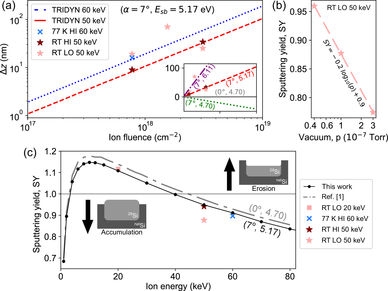
In Fig. 2(a), we show TRIDYN simulations of as a function of ion fluence fitted to experimental data from this work and plotted on a log scale. The experimentally measured values for were obtained through TEM analysis of various SOI samples implanted under different implantation temperatures (RT or 77 K), ion flux (high/HI or low/LO) and energies (50 keV or 60 keV), as described earlier. We note that it was not possible to determine for bulk Si substrates from TEM analysis due to the lack of a buried oxide reference but this should be possible through other surface profiling techniques not performed in this work. As for the simulations, the surface binding energy, , which is the surface potential that an atom has to overcome to escape the surface, was chosen as the fitting parameter. The simulations shown in Fig. 2(a) were calculated assuming eV and a two-layered Si/SiO2 stack. We note that, for 50 keV and 60 keV ions, changing the substrate definition to a single layer of Si increased by less than 1%. This corresponds to a decrease in , which depends linearly on the ion fluence [see Fig. 2], by up to 6% for fluences up to cm-2. The bulk binding energy, , is set to the recommended value of 0 eV in our simulations, [45] noting that setting eV had a similar effect as increasing by 2 %. The displacement threshold energy, , had negligible effect on the simulations performed at 50 keV and 60 keV.
In general, we obtain a reasonable agreement between simulations and our experiments by setting eV, which is a 10% increase from its default value of 4.70 eV. As shown in Fig. 2(a) for 50 keV and 60 keV Si ions, is expected to increase linearly with ion fluence. The large discrepancy between the 50 keV simulated curve (red dashed line) and the 50 keV low flux data points (pink stars) in Fig. 2(a) is due to undesirably high levels of surface contamination from the sample chamber vacuum for these particular implants. Indeed, our experiments indicate that becomes increasingly sensitive to the sample chamber vacuum level as the ion flux decreases. As shown in Fig. 2(b), under low ion flux conditions, we observe a logarithmic relationship between the surface sputtering yield, , and the sample chamber vacuum level, . A decrease in (i.e., increase in ) is observed as the sample chamber background pressure increases, resulting in larger values of . This is due to the incoming flux of residual gas atoms (contamination) approaching the same order of magnitude as the flux of 28Si ions. Thus, accurate modeling of and for a low ion flux and poor vacuum conditions require further adjustments to as illustrated in the inset figure of Fig. 2(a). In the inset figure, we plot on a linear scale the same relationship between and the ion fluence for 50 keV ions but with and set to different values (labeled as ‘’).
Vacuum contamination effects are far less significant under high flux conditions and a reasonable agreement between experiment and simulations is achieved by setting eV as shown in Fig. 2(a). Nevertheless, we believe that the need to increase by 10% from its default value to fit our experimental data is mainly due to low levels of residual gas contamination. Other possible explanations for the need to adjust to fit our experiments (high flux) include modifications to due to surface damage during implantation, [52, 53] higher than expected sample temperatures due to beam heating [26] and a poor thermal conduction between the SOI substrate and sample stage, as well as void swelling effects that we will discuss later.
In Fig. 2(c), we show the TRIDYN simulated relationship for as a function of the ion energy under a fixed ion fluence of cm-2 and corresponding experimental data from this work. Our simulations (black circles) were performed by setting ∘and eV, and assuming a semi-infinite Si substrate. The black curve is a cubic spline fitted to the simulated data to guide the eye. We note that reducing without changing shifts the simulated curve up without significantly changing its lineshape (data not shown for clarity). The sensitivity of and to the choice of and was previously demonstrated in the inset of Fig. 2(a). Importantly, a sputtering yield of one in our simulated curve occurs at 3.3 keV and 40.0 keV. For comparison, we also show another curve (gray dash-dot line) simulated using the same parameters used in Ref. 1 (∘, eV, precision factor 0.1, initial depth interval 0.5 nm, ion fluence cm-2). The one-for-one sputtering mode in this case occurs at 3.0 keV and 44.4 keV ion energies, in good agreement with Ref. 1. Clearly, there is a better agreement between our simulated curve (black line) with our experiments. The large discrepancy observed in the 50 keV low flux experiment (pink star) is attributed to vacuum contamination effects discussed previously.
In short, we show that a better agreement between experiments and simulations can be obtained by making small adjustments to . In the next section [Sec.III.3], we show that the 29Si depletion characteristics from our experiments can also be accurately modeled in TRIDYN by making the same modifications to .
III.3 29Si depletion
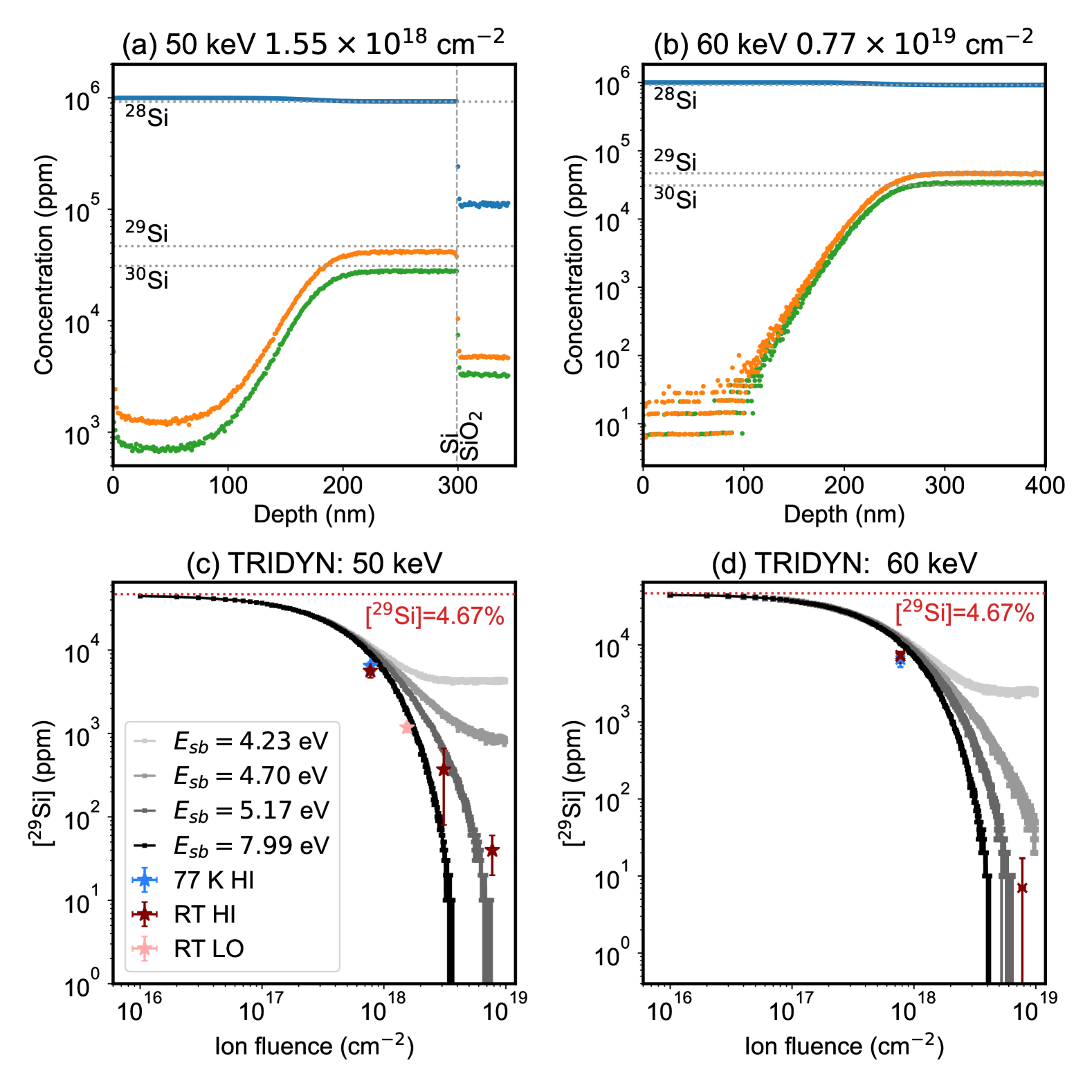
The SIMS measured Si isotopic profiles of selected SOI and Si samples are shown in Figs. 3(a) and (b), respectively. First, we note that the sharp concentration spike in the SIMS profiles at the surface is due to a measurement artifact partly related to the native oxide and transient effects. [54] In Fig. 3(a), the abrupt steps in the concentration profiles at a depth location of around 300 nm are due to measurement of the buried oxide interface in the SOI (note nm in this sample) and are indicated by vertical dashed lines and text labels. In all our samples, the region between the surface and a depth of around 100 nm shows significant depletion of both the 29Si and 30Si isotopes, with a tail extending to around 200 nm before returning to their natural isotopic levels (or very close to it) indicated by the horizontal dotted lines in Fig. 3(a). Note that SIMS measurements on SOI substrates are more susceptible to surface charging and thus are expected to have larger errors than measurement on Si. We believe that this surface charging effect is responsible for the deviation of the 29Si and 30Si concentrations from their natural isotopic level in the deeper regions between 200 nm and 300 nm of the SIMS profiles shown in Fig. 3(a). We define the 29Si (30Si) depletion levels, [29Si] ([30Si]), as the minimum 29Si (30Si) concentration in the sample; for the sample shown in Fig. 3(a), [29Si] = ppm and [30Si] = ppm. On the other hand, the sample shown in Fig. 3(b) is a Si sample implanted under 60 keV cm-2, high flux, RT conditions. Here, both the 29Si and 30Si isotopes were depleted below the SIMS instrument noise floor of approximately 7 ppm. We note that 50 nm of the surface of this sample was oxidized during device fabrication experiments prior to SIMS measurement and the Si isotope profiles shown in Fig. 3(b) exclude this oxidized region (no oxide etching performed). Thus, the expected thickness of the 28Si layer with [29Si] and [30Si] ppm is approximately 150 nm.
In Figs. 3(c) and (d), we plot the TRIDYN curves for [29Si] as a function of ion fluence for 50 keV and 60 keV ion energies, simulated under different values of . Measurements of [29Si] from both SOI and Si samples from our experiments are also shown as scattered data points, where different colors are used to represent the different flux and temperature conditions. A complete data table that summarizes the sample implantation conditions and measured [29Si] levels can be found in the Supplementary Material. We first note that the simulations shown here assume a semi-infinite Si medium (single layer). When simulating 50 keV and 60 keV ions, we observed little to no difference in the [29Si] vs. ion fluence curves when changing the substrate definition to a two-layered Si/SiO2 stack in TRIDYN. Generally, the experimentally measured Si isotope profiles agree with our TRIDYN simulations within one standard error. Larger deviations between experiment and simulations (especially at the tail of the isotopic profiles) are observed when the ion fluence exceeds cm-2, presumably due to vacuum-related contamination. A reasonable agreement between data and simulations is obtained when eV, in good agreement with results from our surface sputtering analyses discussed previously. Importantly, this agreement appears to be independent of the substrate type (Si or SOI). This suggests that local beam heating and thermal conduction to the sample stage play only a minor role (if any) in the 29Si depletion process. Larger discrepancies between experimental and simulated data are observed in samples that were implanted under low flux conditions (for example, the 50 keV cm-2 data point in Fig. 3(c)) due to vacuum contamination effects discussed previously.
For a 60 keV cm-2 implantation, TRIDYN predicts a 29Si depletion of less than 1 ppm, in good agreement with our (noise floor limited) SIMS measurements shown in Fig. 3(b). Additional simulations reveal that 29Si depletion levels of less than 1 ppm can only be achieved when the ion energy results in surface accumulation. As shown in Fig. 2(c), surface accumulation in our experiments occurs when the ion energy is less than 3 keV or higher than 40 keV. Under these ion energy conditions, the 29Si depletion in the sample decreases rapidly as a function of ion fluence and reaches a value of about 1 ppm when the ion fluence is around to cm-2 [details in Supplementary Material]. Furthermore, by increasing the ion energy from 40 keV to 80 keV, the ion fluence required to achieve 29Si depletion levels of 1 ppm or less can be lowered from cm-2 to cm-2. These ion implantation conditions can be easily and realistically achieved as shown by our experiments, demonstrating the competitiveness and attractiveness of our 28Si enrichment process for producing Si spin vacuum substrates required by QIP. In the next section [Sec.III.4], we show that the isotopically enriched 28Si sub-surface layer contains nanoscopic voids that can be easily removed under moderate temperature annealing. The observation of these open volumes was enabled by the gettering of fast diffusing impurities such as gold and copper to the defects during thermal processing, [37] where the fast diffuser was deliberately introduced into the sample surface prior to thermal annealing.
III.4 Open volume defects
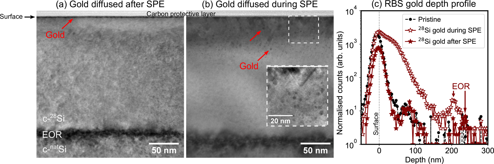
Our experiments indicate that the observation of open volume defects (vacancies or voids) through gold decoration depends crucially on at which stage the gold is introduced. In Fig. 4(a) and (b), we show TEM results from the 28Si enriched bulk Si sample (60 keV cm-2, high flux, RT) where the gold decoration (diffusion anneal) was performed either after or during the SPE annealing stage. Specifically, the sample in Fig. 4(a) was prepared by first performing the SPE anneal (after ion implantation) followed by gold deposition and subsequent annealing to in-diffuse the surface gold. On the other hand, the sample in Fig. 4(b) was prepared by first depositing gold on the sample surface (after ion implantation) followed by SPE annealing. In this case, the gold in-diffusion occurs at the same time as the SPE recrystallization.
In the sample where the gold is diffused into the sample after SPE annealing [Fig. 4(a)], TEM shows a fully recrystallized Si layer (supported by SAED measurements, not shown) with no evidence of gold-decorated open volumes. Rather, the gold appears as a thin dark layer segregated at the surface underneath the carbon protective layer. This is confirmed by RBS profiling of the gold that we will discuss later. On the contrary, in the sample where the gold is in-diffused during the SPE annealing stage [Fig. 4(b)], the open volume defects (voids) can be clearly observed up to a depth of 70 nm from the sample surface. They appear as circular regions of darker contrast in the TEM images due to the high mass contrast of gold (confirmed by energy dispersive X-ray spectroscopy mapping, data not shown) and the gold atoms preferentially clustering within these voids. [35] Two such examples are indicated by the red arrows. The diameter of these voids range from 1 nm to 7 nm. Both the size and density distribution of these gold-decorated voids achieve a maximum at/near the surface and decrease deeper into the sample. These voids are no longer visible under TEM at depth regions beyond 70 nm. Additionally, we also observe stacking-like defects at the surface. An example of this is highlighted by the white dashed region in Fig. 4(b). A higher magnification TEM image of this region is shown in the inset image. These stacking-like defects were not observed in our other samples that were SPE annealed in the absence of gold at the surface [see, for example, Fig. 1(c) and Fig. 4(a)]. Thus, we attribute these stacking defects to the distortion of the SPE planar growth front due to local modifications to the SPE rate in the presence of gold. [55, 23] The dark band of defects located at 200 nm from the surface are the EOR defects, as observed and discussed previously [Fig. 1]. We note that the TEM images shown in Fig. 4(a) and (b) were taken under the same magnification settings and the slight difference (7 nm) in the EOR depth location observed between them can be accounted for by TEM scale calibration errors (5%).
RBS-C measurements of the gold depth profiles in the same gold-decorated 28Si samples shown in Fig. 4(a) and (b) are shown in Fig. 4(c). A reference gold profile obtained from an un-implanted sample (‘Pristine’) diffused with gold under the same annealing conditions (620∘C for 10 min) is also shown. The vertical axis (‘Normalized counts’) is proportional to the gold concentration. In the pristine case, the gold remains predominantly at the surface with a diffusion tail that is 100 times smaller in magnitude that is discernible between the surface and a depth region of 100 nm. This is expected since gold is a fast diffuser and is known to preferentially segregate at the front and back surfaces of Si. [56] We note that the gold surface peak appears slightly broadened at the surface (depth = 0 nm) due to the energy resolution of our RBS detector. On the other hand, the gold distribution for the gold-decorated 28Si samples depends on when the Au diffusion annealing was performed. If the gold diffusion is performed after the SPE annealing step, we observed no significant difference between the pristine sample and 28Si gold profiles (solid black circles and red stars, respectively), except a small gold peak that is observed in the 28Si sample at a depth location greater than 200 nm caused by gold gettering at the EOR defects. The EOR gold gettering peak was observed in both 28Si samples irrespective of when the gold diffusion anneal was performed and is indicated by the arrows and text in Fig. 4(c). The depth location of the EOR gold gettering observed in RBS ( nm) is in good agreement with TEM ( nm).
If the gold diffusion and SPE annealing are performed simultaneously, we observe in RBS significant accumulation of gold between the surface and 50 nm as compared to the pristine sample, with a concentration tail that decreases and extends deeper into the Si layer. Unsurprisingly, the depth region where the gold is accumulating the most (0 to nm) overlaps completely with the TEM depth region where the nanoscopic gold-decorated voids were observed (0 to nm) in Fig. 4(b). Thus, the RBS gold distribution in this sample also reflects the depth profile of the gold-decorated voids. Both of these RBS and TEM observed depth regions are also in good agreement with the calculated depth region for excess vacancies, that is, between the surface and . For the samples shown in Fig. 4, nm and nm calculated from SRIM and TRIDYN, respectively, and thus excess vacancies are expected up to a depth of 60 nm.
Our experiments above suggest that the nanoscopic voids observed in Fig. 4(b) were formed from vacancy excesses during implantation and fully stabilized from gold-vacancy interactions in amorphous Si following 28Si ion implantation. In the sample where the SPE annealing and gold diffusion occurred simultaneously [Fig. 4(b)], the direction of the SPE recrystallization growth front (towards the surface) and gold diffusion (away from the surface) are directly opposite to each other. At an annealing temperature of 620∘C, the SPE growth rate and the diffusion coefficient of gold in amorphous Si are estimated to be 2 nm/s and 1 nm2/s, respectively. [57, 58]. For an a/c-interface (EOR) that is 220 nm deep, the SPE growth front and gold diffusion tail are therefore expected to meet at a depth location of about 48 nm from the surface after 86 s of annealing. Both the further diffusion of gold in crystalline Si beyond the SPE growth front and EOR (towards the Si back surface) and the complete recrystallization of the amorphous Si layer subsequently occur over the remaining annealing duration (about 9 minutes). The competition between gold diffusion and SPE growth and their meeting at around 48 nm may therefore explain the observed abrupt decrease in the gold concentration at 50 nm and the size distribution of the gold-decorated voids in our sample (‘ gold during SPE’).
To obtain a better understanding of the physical origin of these open volumes (vacancies and voids), we performed additional gold decoration experiments on selected 28SOI samples implanted under different temperature and flux conditions where the gold was introduced during the SPE annealing stage. The experimental data for these samples are shown in the Supplementary Material but the key results will be described here. RBS gold profiling indicates that gold had accumulated between the surface and about 50 nm in all of our implanted 28SOI samples. The gold distribution in these samples also appears to depend on the ion flux and sample temperature. Higher fluxes and lower temperatures during implantation result in a higher total gold concentration accumulating below the surface. Indeed, the excess vacancy concentration in the amorphous Si phase is expected to depend on both the ion flux (which dictates the point defect production and clustering rates) and sample temperature (which controls the defect annihilation and clustering rates). Higher stable vacancy excesses due to high ion flux and/or lower sample temperatures may then promote subsequent formation of voids that are revealed by gold decoration during gold diffusion in amorphous Si. [58] Whether the voids are fully formed from vacancy excesses in amorphous Si during implantation, or vacancy/void clustering is enabled by gold interactions is not known. However, we note that even if these open volumes were formed during the ion implantation process, they can be completely removed by a 620∘C 10 minute anneal and are only stabilized by the presence of external impurities such as gold. Further experiments will be required to determine the exact physical origin of these open volumes.
Finally, we note that it may also be possible for the nanoscopic voids and/or high vacancy excesses to cause some degree of surface swelling and a more positive value. Void swelling, as it is termed in the literature, is unfortunately difficult to quantify and is rarely addressed in the published literature. [59, 60, 61] Although these voids can be readily removed by SPE annealing, it may partially account for the observed larger values and the slightly larger surface binding energies required to fit the simulated curve to our experiments.
IV Concluding remarks
Our experiments and simulations demonstrate the ability of the 28Si enrichment process to precisely control the purity of 28Si layers formed on bulk Si and SOI substrates. We note that it was necessary to increase the surface binding energy by 10% to a value of 5.17 eV in TRIDYN to obtain a better agreement with experimentally observed surface sputtering and 29Si depletion characteristics. Key requirements to produce 28Si surface layers with residual 29Si and 30Si concentrations below 1 ppm and at least 100 nm thick include choosing ion implantation energies that result in surface accumulation ( keV or keV) and ion fluences exceeding cm-2. We produce one such sample with 60 keV 28Si ions implanted in bulk Si up to a fluence of cm-2, where the 29Si and 30Si isotopes were depleted to less than 7 ppm, a value limited by our SIMS resolution. Further, our experiments emphasize the importance of performing 28Si enrichment experiments under high vacuum ( Torr) and high ion flux conditions to minimize contamination from background residual gas atoms. High ion fluxes also reduces the overall implantation duration and is desirable for producing samples with larger areas for scaling up. For SOI substrates, high flux ion implantation above A/cm2 performed at RT results in significant broadening of the a/c-interface and interstitial clustering which, after subsequent SPE annealing, resulted in the formation of threading dislocations throughout the 28Si layer. This was not observed in bulk Si substrates and can be circumvented by performing the ion implantation in SOI at 77 K to suppress dynamic annealing. We also report the direct observation of gold-decorated voids in our 28Si samples. The observation of these voids depend critically on when the gold diffusion anneal is performed. In this work, they were only observed when gold is introduced into the amorphous layer during SPE annealing before the growth front catches up to the gold diffusion tail. These voids are no longer visible if the gold atoms are introduced after complete SPE recrystallization of the amorphous implanted layer, which is performed under moderate temperature annealing at 620∘C for 10 minutes. Future low energy positron annihilation spectroscopy experiments may reveal further information related to the excess vacancy distribution in our samples. From a Si device technology and QIP application perspective, our work provides a clear pathway towards realizing large-scale 28Si and 28SOI spin vacuum substrates for ultra-long qubit coherence applications. Spin resonance and qubit spectroscopy experiments are currently underway to uncover the coherent lifetimes of donor qubits embedded in our 28Si and 28SOI substrates.
V Acknowledgments
This research was supported by the Australian Government through the Australian Research Council Centre of Excellence for Quantum Computation and Communication Technology (CE170100012) and Discovery Projects funding scheme (DP220103467). We acknowledge the use of the NCRIS Heavy Ion Accelerator platform (HIA) for access and support to the low energy implanter equipment at the Australian National University, the Bio21 institute for the use of FIB and TEM facilities at the University of Melbourne, and the surface analysis laboratory (SSEAU, MWAC) for access and support to the SIMS equipment at UNSW. TRIDYN calculations were performed with multi-thread parallelization using the Spartan High Performance Computing (HPC) system supported by the University of Melbourne’s Research Computing Services and the Petascale Campus Initiative. SQL and JCM thank Wolfhard Moller, Benoit Voisin, Gabriele de Boo, Alexey Lyasota, and Sven Rogge for useful discussions. We are grateful to Juha Mohonen for providing the SOI substrates.
References
- Holmes et al. [2021] D. Holmes, B. C. Johnson, C. Chua, B. Voisin, S. Kocsis, S. Rubanov, S. Robson, J. C. McCallum, D. R. McCamey, S. Rogge, et al., Isotopic enrichment of silicon by high fluence 28 Si- ion implantation, Physical Review Materials 5, 014601 (2021).
- Acharya et al. [2024] R. Acharya, M. Coke, M. Adshead, K. Li, B. Achinuq, R. Cai, A. B. Gholizadeh, J. Jacobs, J. L. Boland, S. J. Haigh, J. L. Boland, S. J. Haigh, K. L. Moore, D. N. Jamieson, and R. J. Curry, Highly 28Si enriched silicon by localised focused ion beam implantation, Communications Materials 5, 57 (2024).
- Maurand et al. [2016] R. Maurand, X. Jehl, D. Kotekar-Patil, A. Corna, H. Bohuslavskyi, R. Laviéville, L. Hutin, S. Barraud, M. Vinet, M. Sanquer, et al., A CMOS silicon spin qubit, Nature communications 7, 13575 (2016).
- Veldhorst et al. [2017] M. Veldhorst, H. G. J. Eenink, C.-H. Yang, and A. S. Dzurak, Silicon CMOS architecture for a spin-based quantum computer, Nature communications 8, 1766 (2017).
- Gilbert et al. [2020] W. Gilbert, A. Saraiva, W. H. Lim, C. H. Yang, A. Laucht, B. Bertrand, N. Rambal, L. Hutin, C. C. Escott, M. Vinet, and A. S. Dzurak, Single-electron operation of a silicon-CMOS 2 2 quantum dot array with integrated charge sensing, Nano Letters 20, 7882 (2020).
- Morello et al. [2009] A. Morello, C. C. Escott, H. Huebl, L. H. Willems van Beveren, L. C. L. Hollenberg, D. N. Jamieson, A. S. Dzurak, and R. G. Clark, Architecture for high-sensitivity single-shot readout and control of the electron spin of individual donors in silicon, Physical Review B—Condensed Matter and Materials Physics 80, 081307 (2009).
- Tosi et al. [2017] G. Tosi, F. A. Mohiyaddin, V. Schmitt, S. Tenberg, R. Rahman, G. Klimeck, and A. Morello, Silicon quantum processor with robust long-distance qubit couplings, Nature communications 8, 450 (2017).
- Savytskyy et al. [2023] R. Savytskyy, T. Botzem, I. Fernandez de Fuentes, B. Joecker, J. J. Pla, F. E. Hudson, K. M. Itoh, A. M. Jakob, B. C. Johnson, D. N. Jamieson, A. S. Dzurak, and A. Morello, An electrically driven single-atom “flip-flop” qubit, Science advances 9, eadd9408 (2023).
- Yin et al. [2013] C. Yin, M. Rancic, G. G. de Boo, N. Stavrias, J. C. McCallum, M. J. Sellars, and S. Rogge, Optical addressing of an individual erbium ion in silicon, Nature 497, 91 (2013).
- Gritsch et al. [2022] A. Gritsch, L. Weiss, J. Früh, S. Rinner, and A. Reiserer, Narrow optical transitions in erbium-implanted silicon waveguides, Physical Review X 12, 041009 (2022).
- Witzel et al. [2010] W. M. Witzel, M. S. Carroll, A. Morello, Ł. Cywiński, and S. Das Sarma, Electron spin decoherence in isotope-enriched silicon, Physical Review Letters 105, 187602 (2010).
- Itoh and Watanabe [2014] K. M. Itoh and H. Watanabe, Isotope engineering of silicon and diamond for quantum computing and sensing applications, MRS communications 4, 143 (2014).
- Steger et al. [2012] M. Steger, K. Saeedi, M. L. W. Thewalt, J. J. L. Morton, H. Riemann, N. V. Abrosimov, P. Becker, and H.-J. Pohl, Quantum information storage for over 180 s using donor spins in a 28si “semiconductor vacuum”, Science 336, 1280 (2012).
- Becker et al. [2010] P. Becker, H.-J. Pohl, H. Riemann, and N. Abrosimov, Enrichment of silicon for a better kilogram, physica status solidi (a) 207, 49 (2010).
- Abrosimov et al. [2017] N. V. Abrosimov, D. G. Aref’Ev, P. Becker, H. Bettin, A. D. Bulanov, M. F. Churbanov, S. V. Filimonov, V. A. Gavva, O. N. Godisov, A. V. Gusev, T. V. Kotereva, D. Nietzold, M. Peters, A. M. Potapov, H.-J. Pohl, A. Pramann, H. Riemann, P.-T. Scheel, R. Stosch, S. Wundrack, and S. Zakel, A new generation of 99.999% enriched 28Si single crystals for the determination of Avogadro’s constant, Metrologia 54, 599 (2017).
- Ager et al. [2005] J. W. Ager, J. W. Beeman, W. L. Hansen, E. E. Haller, I. D. Sharp, C. Liao, A. Yang, M. L. W. Thewalt, and H. Riemann, High-purity, isotopically enriched bulk silicon, Journal of the Electrochemical Society 152, G448 (2005).
- Mazzocchi et al. [2019] V. Mazzocchi, P. G. Sennikov, A. D. Bulanov, M. F. Churbanov, B. Bertrand, L. Hutin, J. P. Barnes, M. N. Drozdov, J. M. Hartmann, and M. Sanquer, 99.992% 28Si CVD-grown epilayer on 300 mm substrates for large scale integration of silicon spin qubits, Journal of Crystal Growth 509, 1 (2019).
- Liu et al. [2022] Y. Liu, S. Rinner, T. Remmele, O. Ernst, A. Reiserer, and T. Boeck, 28Silicon-on-insulator for optically interfaced quantum emitters, Journal of Crystal Growth 593, 126733 (2022).
- Itoh et al. [2003] K. M. Itoh, J. Kato, M. Uemura, A. K. Kaliteevskii, O. N. Godisov, G. G. Devyatych, A. D. Bulanov, A. V. Gusev, I. D. Kovalev, P. G. Sennikov, H.-J. Pohl, N. V. Abrosimov, and H. Riemann, High purity isotopically enriched 29Si and 30Si single crystals: Isotope separation, purification, and growth, Japanese Journal of Applied Physics 42, 6248 (2003).
- Devyatykh et al. [2008] G. G. Devyatykh, A. D. Bulanov, A. V. Gusev, I. D. Kovalev, V. A. Krylov, A. M. Potapov, P. G. Sennikov, S. A. Adamchik, V. A. Gavva, A. P. Kotkov, M. F. Churbanov, E. M. Dianov, A. K. Kaliteevskii, O. N. Godisov, H. J. Pohl, P. Becker, H. Riemann, and N. V. Abrosimov, High-purity single-crystal monoisotopic silicon-28 for precise determination of Avogadro’s number, Doklady Chemistry 421, 157 (2008).
- Klos et al. [2024] J. Klos, J. Tröger, J. Keutgen, M. P. Losert, N. V. Abrosimov, J. Knoch, H. Bracht, S. N. Coppersmith, M. Friesen, O. Cojocaru-Mirédin, L. R. Schreiber, and D. Bougeard, Atomistic Compositional Details and Their Importance for Spin Qubits in Isotope-Purified Silicon Quantum Wells, Advanced Science 11, 2407442 (2024).
- Becker [2012] P. Becker, The new kilogram definition based on counting the atoms in a 28si crystal, Contemporary Physics 53, 461 (2012).
- Johnson et al. [2015] B. C. Johnson, J. C. McCallum, and M. J. Aziz, Solid-phase epitaxy, in Handbook of Crystal Growth (Elsevier, 2015) pp. 317–363.
- Radek et al. [2015] M. Radek, H. Bracht, B. C. Johnson, J. C. McCallum, M. Posselt, and B. Liedke, Atomic transport during solid-phase epitaxial recrystallization of amorphous germanium, Applied Physics Letters 107, 082112 (2015).
- Bracht et al. [1998] H. Bracht, E. E. Haller, and R. Clark-Phelps, Silicon self-diffusion in isotope heterostructures, Physical Review Letters 81, 393 (1998).
- Holland et al. [1996] O. W. Holland, L. Xie, B. Nielsen, and D. S. Zhou, Implantation of Si under extreme conditions: the effects of high temperature and dose on damage accumulation, Journal of electronic materials 25, 99 (1996).
- Williams et al. [1983] J. S. Williams, D. J. Chivers, R. G. Elliman, S. T. Johnson, E. M. Lawson, I. V. Mitchell, K. G. Orrman-Rossiter, A. P. Pogany, and K. T. Short, The Production of Porous Structures on Si, Ge and GaAs by High Dose Ion Implantation, MRS Online Proceedings Library (OPL) 27, 205 (1983).
- Williams [1994] J. S. Williams, Ion Induced Damage and Dynamic Annealing Processes, in Laser and Ion Beam Modification of Materials (Elsevier, 1994) pp. 417–423.
- Zhu et al. [1997] X. Zhu, J. S. Williams, D. J. Llewellyn, and J. C. McCallum, Microstructure of Ultra High Dose Self Implanted Silicon, MRS Online Proceedings Library 504, 27 (1997).
- Goldberg et al. [1999] R. D. Goldberg, J. S. Williams, and R. G. Elliman, Preferential amorphization at extended defects of self-ion-irradiated silicon, Physical Review Letters 82, 771 (1999).
- Mazzone [1986] A. M. Mazzone, Defect distribution in ion-implanted silicon, Physica Status Solidi. A, Applied Research 95, 149 (1986).
- Pellegrino et al. [2001] P. Pellegrino, P. Leveque, J. Wong-Leung, C. Jagadish, and B. G. Svensson, Separation of vacancy and interstitial depth profiles in ion-implanted silicon: Experimental observation, Applied Physics Letters 78, 3442 (2001).
- Brown et al. [1998] R. A. Brown, O. Kononchuk, G. A. Rozgonyi, S. Koveshnikov, A. P. Knights, P. J. Simpson, and F. Gonzalez, Impurity gettering to secondary defects created by MeV ion implantation in silicon, Journal of Applied Physics 84, 2459 (1998).
- Venezia et al. [1998] V. C. Venezia, D. J. Eaglesham, T. E. Haynes, A. Agarwal, D. C. Jacobson, H.-J. Gossmann, and F. H. Baumann, Depth profiling of vacancy clusters in MeV-implanted Si using Au labeling, Applied Physics Letters 73, 2980 (1998).
- Williams et al. [2001] J. S. Williams, M. J. Conway, B. C. Williams, and J. Wong-Leung, Direct observation of voids in the vacancy excess region of ion bombarded silicon, Applied Physics Letters 78, 2867 (2001).
- Peeva et al. [2000] A. Peeva, R. Koegler, G. Brauer, P. Werner, and W. Skorupa, Metallic impurity gettering to defects remaining in the RP/2 region of MeV-ion implanted and annealed silicon, Materials Science in Semiconductor Processing 3, 297 (2000).
- Williams and Wong-Leung [2009] J. S. Williams and J. Wong-Leung, Voids and nanocavities in silicon, Materials Science with Ion Beams , 113 (2009).
- Zhu et al. [1999] X. Zhu, J. S. Williams, D. J. Llewellyn, and J. C. McCallum, Instability of nanocavities in amorphous silicon, Applied Physics Letters 74, 2313 (1999).
- Zhu et al. [2001] X. F. Zhu, J. S. Williams, M. J. Conway, M. C. Ridgway, F. Fortuna, M.-O. Ruault, and H. Bernas, Direct observation of irradiation-induced nanocavity shrinkage in Si, Applied Physics Letters 79, 3416 (2001).
- Kudriavtsev et al. [2020] Y. Kudriavtsev, A. Hernandez-Zanabria, C. Salinas, and R. Asomoza, The formation of porous silicon by irradiation with low-energy ions, Vacuum 177, 109393 (2020).
- Aspelmeyer et al. [2014] M. Aspelmeyer, T. J. Kippenberg, and F. Marquardt, Cavity optomechanics, Reviews of Modern Physics 86, 1391 (2014).
- Kumar et al. [2022] A. S. Kumar, J. Nätkinniemi, H. Lyyra, and J. T. Muhonen, Single-laser feedback cooling of optomechanical resonators, arXiv preprint arXiv:2209.06029 (2022).
- Doolittle [1985] L. R. Doolittle, Algorithms for the rapid simulation of Rutherford backscattering spectra, Nuclear Instruments and Methods in Physics Research Section B: Beam Interactions with Materials and Atoms 9, 344 (1985).
- Ziegler et al. [2008] J. F. Ziegler, J. P. Biersack, M. D. Ziegler, et al., The stopping and range of ions in matter (SRIM Chester, Maryland, 2008).
- Möller et al. [1988] W. Möller, W. Eckstein, and J. P. Biersack, Tridyn-binary collision simulation of atomic collisions and dynamic composition changes in solids, Computer Physics Communications 51, 355 (1988).
- Custer et al. [1994] J. S. Custer, M. O. Thompson, D. Jacobson, J. M. Poate, S. Roorda, W. C. Sinke, and F. Spaepen, Density of amorphous Si, Applied Physics Letters 64, 437 (1994).
- Note [1] Derived assuming a Si atomic density of atoms/cm3 and when the sputter yield is zero, nm for an ion fluence of cm-2.
- Woo et al. [2016] S. Woo, M. Bertoni, K. Choi, S. Nam, S. Castellanos, D. M. Powell, T. Buonassisi, and H. Choi, An insight into dislocation density reduction in multicrystalline silicon, Solar Energy Materials and Solar Cells 155, 88 (2016).
- Haunschild et al. [2010] J. Haunschild, M. Glatthaar, M. Demant, J. Nievendick, M. Motzko, S. Rein, and E. R. Weber, Quality control of as-cut multicrystalline silicon wafers using photoluminescence imaging for solar cell production, Solar Energy Materials and Solar Cells 94, 2007 (2010).
- Arguirov et al. [2009] T. Arguirov, T. Mchedlidze, M. Kittler, M. Reiche, T. Wilhelm, T. Hoang, J. Holleman, and J. Schmitz, Silicon based light emitters utilizing radiation from dislocations; electric field induced shift of the dislocation-related luminescence, Physica E: Low-dimensional Systems and Nanostructures 41, 907 (2009).
- Stowe et al. [2003] D. J. Stowe, S. A. Galloway, S. Senkader, K. Mallik, R. J. Falster, and P. R. Wilshaw, Near-band gap luminescence at room temperature from dislocations in silicon, Physica B: Condensed Matter 340, 710 (2003).
- Sigmund [1969] P. Sigmund, Theory of sputtering. I. Sputtering yield of amorphous and polycrystalline targets, Physical Review 184, 383 (1969).
- Almén and Bruce [1961] O. Almén and G. Bruce, Sputtering experiments in the high energy region, Nuclear Instruments and Methods 11, 279 (1961).
- Stevie [2005] F. A. Stevie, Focused ion beam secondary ion mass spectrometry (FIB-SIMS), Introduction to Focused Ion Beams: Instrumentation, Theory, Techniques and Practice , 269 (2005).
- Jacobson et al. [1986] D. C. Jacobson, J. M. Poate, and G. L. Olson, Zone refining and enhancement of solid phase epitaxial growth rates in Au-implanted amorphous Si, Applied Physics Letters 48, 118 (1986).
- Graff [2013] K. Graff, Metal impurities in silicon-device fabrication, Vol. 24 (Springer Science & Business Media, 2013).
- Roth et al. [1990] J. A. Roth, G. L. Olson, D. C. Jacobson, and J. M. Poate, Kinetics of solid phase epitaxy in thick amorphous Si layers formed by MeV ion implantation, Applied Physics Letters 57, 1340 (1990).
- Frank et al. [1996] W. Frank, W. Gustin, and M. Horz, Diffusion of gold and platinum in amorphous silicon and germanium, Journal of non-crystalline solids 205, 208 (1996).
- Wang et al. [2016] J. Wang, M. B. Toloczko, N. Bailey, F. A. Garner, J. Gigax, and L. Shao, Modification of SRIM-calculated dose and injected ion profiles due to sputtering, injected ion buildup and void swelling, Nuclear Instruments and Methods in Physics Research Section B: Beam Interactions with Materials and Atoms 387, 20 (2016).
- Getto et al. [2016] E. Getto, K. Sun, S. Taller, A. M. Monterrosa, Z. Jiao, and G. S. Was, Methodology for determining void swelling at very high damage under ion irradiation, Journal of Nuclear Materials 477, 273 (2016).
- David et al. [2008] C. David, B. K. Panigrahi, S. Balaji, A. K. Balamurugan, K. G. M. Nair, G. Amarendra, C. S. Sundar, and B. Raj, A study of the effect of titanium on the void swelling behavior of D9 steels by ion beam simulation, Journal of Nuclear Materials 383, 132 (2008).