Abstract
Measurement of signals generated by superconducting Josephson junction (JJ) circuits require ultra-fast components located in close proximity to the generating circuitry. We report a detailed study of optimal design criteria for a JJ-based sampler which balances the highest sampler bandwidth (shortest 10%–90% rise time) with minimal sampled waveform distortion. We explore the impacts on performance of a sampler, realized using a single underdamped JJ as the logical sampling element (the comparator), due to the type of signal-comparator coupling scheme that is utilized (galvanic, inductive, or capacitive). In these simulations we emulate the entire waveform reconstruction sampling process, via comparator threshold detection, while sweeping the time location at which the waveform is being sampled. We extract the sampled waveform rise time (or FWHM) as a function of the comparator’s Stewart-McCumber parameter and as a function of the coupling strength between the device under test and comparator. Based on our simulation results we design, fabricate, and characterize a cryocooled (3.6 K operating temperature) JJ sampler utilizing the NIST state-of-the-art Nb/amorphous-Si/Nb junctions. We separately sample a step signal and impulse generator co-located on-chip with the comparator and sampling strobe generator by implementing the same binary search comparator threshold detection technique during sampler operation as is used in simulation. With this technique the system is fully-digital and automated and operation of the fabricated device directly mirrors simulation. Our sampler technology shows a 10%–90% rise time of 3.3 ps and the capability to measure transient pulse widths of 2.5 ps FWHM. A linear systems analysis of sampled waveforms indicate a 3 dB bandwidth of 225 GHz, but we demonstrate effective measurement of signals well above this – as high as 600 GHz.
I Introduction
Circuits based on superconducting Josephson junctions (JJs) have wide applications ranging from signal metrology Rüfenacht, Flowers-Jacobs, and Benz (2018); Bauer et al. (2022), low-noise amplification Castellanos-Beltran and Lehnert (2007); Roy and Devoret (2018); Macklin et al. (2015), to novel computation (superconducting super- Fourie (2018); Fourie et al. (2019) and quantum- computers Blais et al. (2021); Krantz et al. (2019); Leonard et al. (2019); Howe et al. (2022); Castellanos-Beltran et al. (2023)) arising from their low power consumption, the nonlinear Josephson inductance, and area quantization of the single flux quantum (SFQ) pulses they can generate. Metrology of signal waveforms generated by JJ-based circuits is challenging due to the short duration of an SFQ pulse (a few picoseconds), and the fact the circuits are embedded in cryogenic systems – precluding direct access using short cabling lengths. Despite these challenges, JJ-based samplers have successfully been used to diagnose operation of complex superconducting circuits via integration at key circuit nodes Ketchen, Herrell, and Anderson (1985).
To minimize dispersion, and thus faithfully detect JJ-generated signals, an appropriate measurement technology must be located in close proximity to the superconducting circuits. An obvious choice is to incorporate a single JJHamilton (1979); Wolf, Van Zeghbroeck, and Deutsch (1985); Van Zeghbroeck (1985) or superconducting quantum interference device (SQUID) Faris (1979) as a logical comparator on the same chip with the target circuitry. This strategy is beneficial in terms of ease-of-integration – the sampler can be co-fabricated on the same chip as the device under test (DUT) – and simplicity of the experimental setup. Furthermore, this strategy provides a wide parameter space for the DUT-comparator coupling in terms of strength and type – galvanic, inductive, or capacitive – which can be easily defined and fixed during the design and fabrication phases.
Electro-optic (EO) sampling strategies Kolner and Bloom (1986); Seitz et al. (2006); Wang et al. (1995) present another viable path to sampling waveforms generated by superconducting circuits and, due to the femtosecond timescale routinely available in pulsed laser systems today, can potentially offer rise times beyond that available to Nb-based superconducting samplers Hegmann et al. (1995); Keil and Dykaar (1992). However, a major limitation of EO sampler implementations arises from the need to incorporate an EO transduction element such as lithium- or niobium-tantalate. These transduction elements typically have large dielectric constants, e.g. for LiTaO3 Kolner and Bloom (1986), and are frequently coupled to the electric field in an on-chip microwave transmission line, resulting in significant distortion of the target waveform (signal). Multiple reflections of the laser pulse from the substrate’s top and bottom surfaces also confound the goal of low-distortion sampling Seitz et al. (2006); Kolner and Bloom (1986). A final concern is the interplay between the EO sensitivity (or signal-to-noise ratio) and laser power, which has the potential for significant quasiparticle generation and degradation of the performance of the superconducting DUT circuitry. Nonetheless, EO sampling is a demonstrated technique for measurement of JJ-generated signals – e.g. SFQ pulses Wang et al. (1995).
Initial JJ sampler efforts focused on Nb-based underdamped (latching) junctions, i.e. with Stewart-McCumber parameter Wolf, Van Zeghbroeck, and Deutsch (1985); Tuckerman (1980); Faris (1980); Whiteley et al. (1988); Akoh et al. (1983, 1985); Sakai, Akoh, and Hayakawa (1983); Harris, Wolf, and Moore (1982), which still hold the highest bandwidth and shortest rise time of all clearly-demonstrated sampling techniques Wolf, Van Zeghbroeck, and Deutsch (1985). In the late 1980s, a commercial sampling oscilloscope and time domain reflectometer with advertised 70 GHz bandwidth and 5 ps risetime was developed based on this technologyWhiteley (1988); Andrews (1989); Whiteley et al. (1988) – however these bandwidths and rise times are insufficient for our applications targeting precision voltage metrology of circuits with rise times and pulse FHWM of ps. More recent efforts have been made using high temperature superconductors (HTSs) Maruyama et al. (2005); Hidaka et al. (1999) in attempts to leverage the increased gap frequency Suzuki et al. (2005) to yield a faster sampler response Maruyama et al. (2007). Because these realizations of HTS JJs were intrinsically shunted, and either critically- () or over-damped (), a latching comparator could not be implemented. Instead, it was necessary to incorporate additional complexity in the form of SFQ-to-dc readout SQUIDs to determine comparator switching. As we will show in Sec. III.1, shunting JJs into the critically-damped regime also increases their switching time and limits the bandwidth of such a sampler. Indeed, damping in HTS JJ samplers has served to significantly reduce the achieved bandwidth compared to expectations based simply on the increased gap frequency.
The ultimate goal of our sampler development lies in voltage and waveform metrology of JJ-based circuits generating signals with characteristic timescales of a few picoseconds, so the target sampling technology must have similar rise times and dynamic bandwidths of hundreds of gigahertz – ideally faster and wider bandwidth than the target circuitry. To this end we pursue a latching JJ sampler co-located with the target-signal-generating circuits as this technology possesses the most straightforward, and flexible path to high-bandwidth, low-distortion sampling. Using NIST’s state-of-the-art JJ process using Nb electrodes and amorphous-silicon (a-Si) barriers Olaya et al. (2023a, b) we design a sampler prototype similar to [(15)] and demonstrate this strategy has sufficient speed for measuring circuits based on SFQ pulses.
In this paper we present both simulations and test results of sampling the picosecond-duration output waveforms of two different DUTS with all JJs realized using underdamped (latching) Nb/a-Si/Nb JJs with a critical current density, , of 0.22 mA/m2. We demonstrate a novel technique for comparator threshold detection using a binary search that we apply in both simulation of the full sampling operation and measurement of fabricated devices. This allows us to fully simulate the entire sampling process in the same manner it is performed in the laboratory – for the first time ever in Josephson sampler technology – and enables strong agreement between our modeling and measurement results. In Sec. II we first review the operation of a latching Josephson sampler. In Sec. III we simulate a JJ sampler comprised of a single comparator with a critical current mA, a pulse-generating strobe circuit, and the circuit generating the target signal (the DUT). The first DUT that we consider outputs a step signal and the second outputs a finite-duration impulse. We implement these circuits in simulation with physically realizable components: a latching SQUID for the step signal DUT, and a Faris pulser Faris (1980) for the impulse generator DUT Wolf, Van Zeghbroeck, and Deutsch (1985). We will show there exists an interplay between the intrinsic sampler rise time / bandwidth and the dynamics of the DUT used to characterize it. In Sec. IV we describe our experimental setup and present cryogenic measurements of sampler devices operated at 3.6 K for both the step function and impulse DUTs. Sec. V details a first-order linear systems analysis to extract an approximate sampler bandwidth. Additional simulation and measurement details are included in the Appendices.
II Latching Josephson Sampler Operation
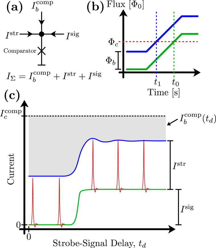
The principle of operation of a latching Josephson sampler is shown in Fig. 1. A JJ with a large critical current, (the comparator) is dc-biased with current . The comparator is attached to an on-chip sampling pulse generator, the strobe, and a number of DUT circuits. The comparator and the strobe generator make up the sampler; where the strobe is used to selectively drive the total comparator current above at a specified time. In general, only a single DUT circuit is operated and sampled at a time. When the sum () of the dc bias (), the strobe current pulse (), and the DUT signal () exceeds the comparator (the threshold), the comparator voltage rapidly latches to the superconducting gap voltage. In this way, the entire DUT signal waveform can be sampled by changing the delay of the strobe relative to the DUT signal, as illustrated in Fig 1. The comparator remains latched at the Nb gap voltage of 2.8 mV until is dropped below the comparator return current – making it an experimentally straightforward task to both determine whether the comparator has latched and to reset it for the next sampling event. We define the interval between setting and resetting all biases, during which the strobe and DUT are triggered and the comparator is allowed to latch (depending on ), as a sampling period. Due to this required reset, the dc biases are actually square pulses.
Latching JJ samplers have historically operated with sampling periods on the order of a few microseconds inside a slower feedback loop (with integration times 0.1 s–1 s) configured to maintain the total current into the comparator exactly at on slow timescalesWolf, Van Zeghbroeck, and Deutsch (1985); Tuckerman (1980); Whiteley et al. (1988); Akoh et al. (1983); Askerzade (2006). A secondary bias current is typically applied at the slower timescale which sweeps the relative delay between triggering the strobe and DUT by causing one to generate its waveform slightly earlier on the rising edge of the flux pulse. Thus the sweep bias causes the strobe and signal to traverse one another at the slower integrator feedback timescale, resulting in full sampling of the target waveform at the sweep generator frequency.
Note that the purpose of the integrator feedback is to determine the change in bias required to latch the comparator at a given relative timing delay, shown as the gray region in Fig. 1, due to the value of the target signal when the strobe arrives. In this work, we omitted the sweep bias and feedback loop in favor of a digitizer and two programmable current sources. One current source is used to first set a fixed delay by setting a small added current bias to the DUT flux trigger. Then the digitizer timestream mean voltage – windowed over a portion of a single sampling period after the strobe is known to have triggered – can be used as a simple metric to determine if the comparator has latched. The second current source, supplying , is dithered to determine the (e.g. 50%) latching threshold for each programmed delay. In practice we implement a binary search algorithm to determine . This experimental procedure is deliberately chosen to mirror the simulation strategy described in the following section to permit us to much more accurately simulate experimentally-realized samplers Van Zeghbroeck, Howe, and Hopkins (2024).
III Sampler Performance Simulations
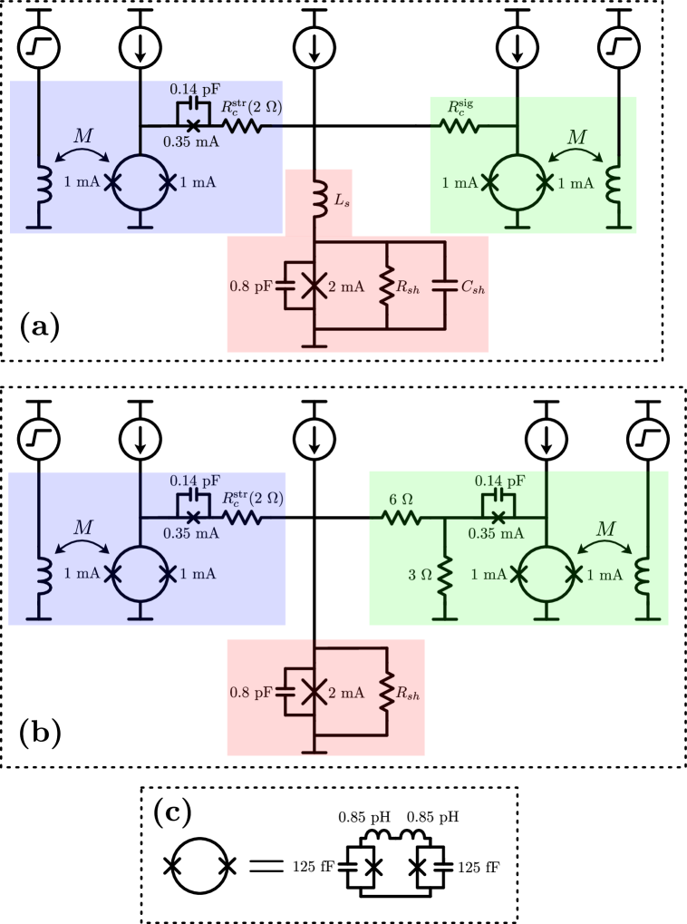
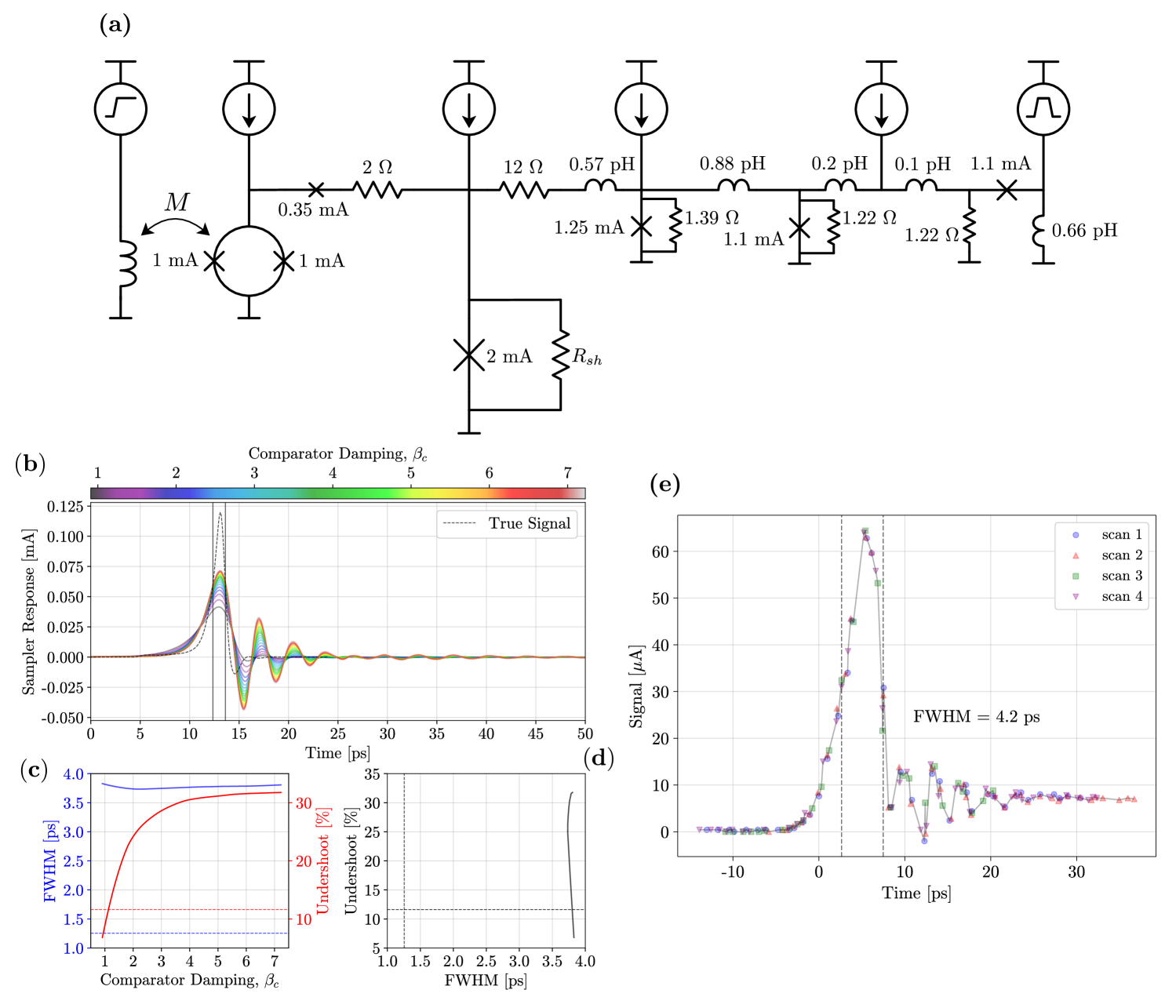
Simulations of the ideal and ultimate JJ sampler performance using a delta function strobe and zero-rise-time step signal have recently been performed Van Zeghbroeck, Howe, and Hopkins (2024); Van Zeghbroeck (2024) so here we focus on physically realizable circuits and signals. To extract rise time we simulate the circuit shown in Fig. 2(a) – where the DUT is a latching SQUID. To simulate sampling of a finite-duration pulse we use the circuit shown in Fig. 2(b). For a step signal the important metrics are the 10%–90% rise time – defined as the rise time, – and the distortion of the sampled signal – which is quantified as the overshoot during the initial rise in sampler signal relative to the asymptotic, or steady-state, sampler response after the SQUID has latched Åström and Murray (2007). When considering the response for imaging an impulse we consider the full width at half maximum (FWHM) and the undershoot following the main peak to benchmark performance. In both cases there is an effective speed limit imposed by the intrinsic dynamics of the target signal generators beyond which the sampler cannot be characterized. For the step signal DUT this is the 10–90% rise time of the SQUID itself, and for the impulse generator DUT this is the FWHM of the Faris pulser pulse directly at its output. These effects are due to the fact that the sampler output is the convolution of the comparator response and the DUT signal.
We use the WRspice circuit simulation package NIS ; wrs to perform our simulations and use the built-in resistive- and capacitively-shunted junction (RCSJ) model. We choose the WRspice quasiparticle model giving a quasiparticle contribution with an exponential dependence on the bias current wrs ; xic ; Fourie (2018). We use JJ parameters characteristic to our Nb/a-Si/Nb fabrication process Olaya et al. (2019) (Appendix C): a specific capacitance of 80 fF/m2, characteristic voltage of mV, and a subgap resistance of 60 . We remove the implicit JJ shunts in WRspice and provide explicit shunts in the circuit definition when needed. To determine the threshold comparator bias at each strobe-signal delay we implement a binary search technique in which only single sampling periods at a time are simulated and comparator latching is determined by a simple voltage threshold in the absence of noise (see Appendix A).
III.1 Step Signal Response
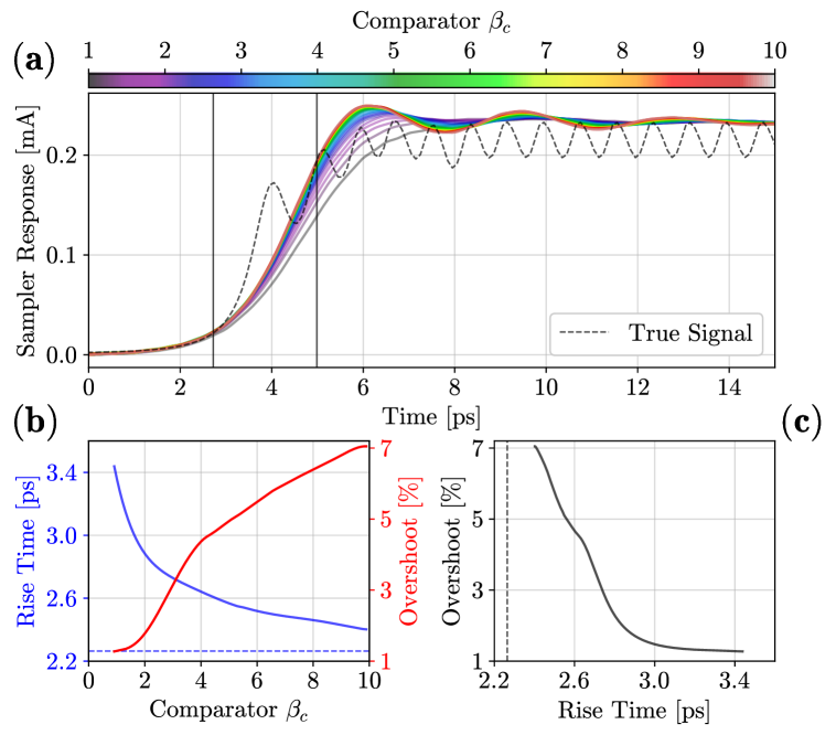
First we consider the sampler dynamics when sampling the step signal created by the latching SQUID, shown in Fig. 2(a), while various circuit parameters are swept. As previously mentioned, the goal of this study is to determine optimal design considerations for a JJ sampler – specifically in terms of an ideal target for the comparator Stewart-McCumber parameter in the presence of an external coupling network , and the most favorable signal coupling method: galvanic, capacitive, or inductive. Here and are the equivalent capacitance and resistance shunting the comparator due to the addition of the connected circuits in Fig. 2. First we perform a sweep, by tuning the value of the explicit comparator shunt resistor , and extract and the overshoot from the sampled output waveform. The comparator is , and is thus effectively bounded above by for our case. Results of this simulation sweep are shown in Fig. 3 and reveal a clear tradeoff between minimal distortion sampling of the SQUID signal and the rise time. Indeed, low-distortion sampling – corresponding to an overshoot of – requires a nearly critically-damped comparator. Given the weaker relation between and it is more favorable to enforce , as this is effectively the “knee" in Fig. 3(b,c) above which small gains in rise time result in significant distortion of the signal when sampled.
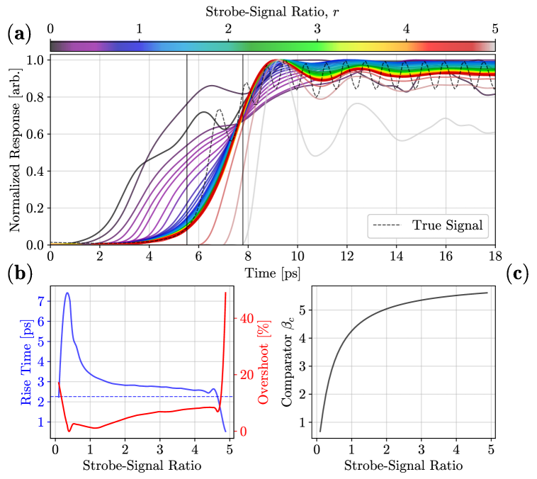
The next obvious question in Josephson sampler design is how large the relative amplitudes of the strobe and signal should be. Previous Josephson sampler implementationsFaris (1980); Maruyama et al. (2007); Tuckerman (1980) have operated with strobe-to-signal ratios, , from unity to over 10 – with the most successful samplerWolf, Van Zeghbroeck, and Deutsch (1985) possessing two DUTs with strobe-to-signal ratios of and . To determine the sampler response as a function of the strobe-to-signal ratio we choose the coupling resistor as our free parameter and conduct a rise time simulation, as detailed above, and with (maximum ). For these simulations, because we sweep over an order of magnitude, the amount of SQUID bias current which branches upon latching of the SQUID and is then injected into the comparator is significant. This reduces the amplitude of the signal current relative to the full range of comparator bias needed to ensure never latches the comparator while always latches. To compensate for these effects we peak-normalize the sampler output for each trace.
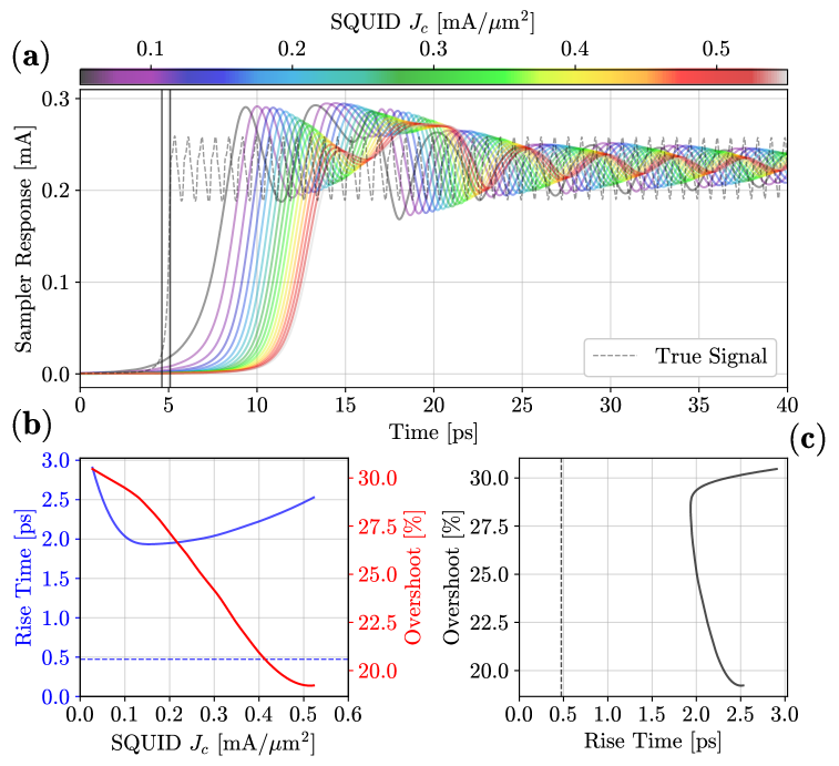
Fig. 4 shows the simulated sampler output while varying . Significant signal distortion and degradation in the rise time is evident in Fig. 4(a) for . Additionally, for we see that the sampler is unable to reconstruct the target signal with appreciable fidelity. This is due to the finite, non-zero tail produced by Faris pulsers, i.e. the strobe, implemented with large sub-gap resistance JJs Cui et al. (2017). When the relative height of the strobe’s post-pulse tail is approximately equal to the SQUID DUT signal amplitude the sampler instead attempts to measure both the target waveform and the strobe pulse tail simultaneously. Our cutoff of indicates the post-pulse tail amplitude is approximately 1/5th the peak pulse height, which is in good agreement with the strobe Faris pulser output seen in simulation. Clearly, for our implementation, the strobe-signal ratio has an optimum value of 2–3 as this optimizes the rise time while allowing variation in without compromising performance.
III.1.1 High Current Density JJs: Faster DUTs and Sampler
The extracted sampler rise times in the simulations in Sec. III.1 are a result of the convolution of the sampler response and the finite-width of the SQUID DUT step-function outputMaruyama et al. (2007). The sampler response is limited by the comparator dynamics and the finite-width of the strobe pulse; both can be improved by increasing the ratio of the critical current to junction capacitance, as shown elsewhereVan Zeghbroeck, Howe, and Hopkins (2024); Van Zeghbroeck (2024, 1985); Harris (1979); Whiteley et al. (2023). The rise time of the SQUID DUT output is limited by the SQUID Harris, Wolf, and Moore (1982); Van Zeghbroeck (2024) and both the and rise times. The relevant resistances for are both the SQUID normal resistance and the DUT-comparator coupler .
Here we explore the feasibility of creating a real circuit (DUT) which could be used to measure the true ultimate rise time of the comparator. Namely we explore avenues to increase the SQUID latching speed, while making no changes to the comparator+strobe (sampler) circuit, and test whether we can observe improved sampled rise times compared to those presented in Sec. III.1. Decreasing the SQUID self-inductance, , and JJ capacitance yields a significantly faster SQUID response. In our simulations we can reduce the SQUID switching time by over a factor of 4.5, resulting in a 10%–90% rise time of 0.47 ps, by lowering to 0.19 pH and the SQUID JJ capacitance to 50 fF. These values are a reduction by a factor of 10 and 2.5 relative to and used in Sec. III.1, respectively. Both reductions are physically possible by (a) moving to a geometry where the SQUID loop axis is in the plane of the substrate rather than orthogonal Wolf, Van Zeghbroeck, and Deutsch (1985), and (b) varying the JJ process critical current density Olaya et al. (2023a) at fixed specific capacitance (80 fF/m2).
We simulated the sampled rise time of this faster SQUID DUT, fixing at 0.19 pH and sweeping the SQUID while the sampler circuit remained unchanged ( held fixed at 0.2 mA/m2). In WRspiceNIS this is accomplished by fixing and sweeping the JJ self-capacitance – i.e. a JJ fabricated in a higher process will have a smaller area for a fixed and thus a smaller capacitance. Fig. 5 shows the results of this “multi-" device with a comparator of 10 (fastest sampler response of Fig. 3). We observe from these results that, even with the SQUID a factor of two below our original design point of 0.2 mA/m2, the reduction in still allows us to measure and demonstrate a sampler which is faster than that obtained in the simulations of Sec. III.1; note however, that without changing the sampler circuit parameters, the minimum measured rise time is ps even with a SQUID rise time of ps. Thus we may interpret these results as revealing the intrinsic sampler rise time is approximately 1.9 ps
The dependence of the minimum quantifiable sampler rise time on the SQUID is nontrivial and is actually deleterious once the SQUID exceeds mA/m2. I.e., the most fruitful path to produce a DUT whose rise time is less than the intrinsic comparator capability, and guarantees we may fully explore this contribution to the sampler’s , is to reduce the SQUID self-inductance. Of course, care must be taken to produce DUTs whose response is fast enough that the ultimate limiting behavior of the sampler (and not the DUT-sampler system convolution) may be faithfully characterized. Co-fabricating a DUT with a higher than that of the comparator is purely a technique for extracting the intrinsic sampler rise time and bandwidth, at a cost of more processing steps, and is not of large practical import.
III.2 Finite Impulse Response
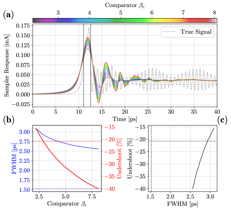
To conclude our design studies of latching JJ samplers we focus on the sampler’s finite impulse response – in this case realized using a Faris pulser identical to the strobe generator and coupled to the comparator using a current divider comprised of a 6 series resistance, and 3 parallel resistance to ground. The current divider is chosen to make for the Faris pulser DUT and strobe approximately the same while enforcing a strobe-signal ratio of . Here we perform a single comparator sweep and characterize the reconstructed waveform FWHM and undershoot. Fig. 6 shows a much higher sensitivity to signal distortion at the sampler output relative to the SQUID DUT step signal response case. While the sampled Faris pulser pulse FWHM is nearly static as is tuned, significant improvement in distortion is achieved when the comparator is close to critically damped.
III.3 Reactive Coupling
Leveraging the learnings of Sec. III.1 we conclude that an optimally flexible JJ sampler, capable of reconstructing the fastest signals with minimal distortion is achieved when –4 and with a strobe-signal ratio of 2–3. However, this is in the case of galvanically-coupled DUTs. It is certainly possible to reactively-couple the DUTs using either capacitors in parallel or inductors in series with the comparator ( and in Fig. 2(a)). Such a coupling scheme is attractive in scenarios where the sampler and DUTs are housed on separate chips – such as a scanning SQUID sampler Cui et al. (2017) or in the case of a flip-chip bonded sampler-DUT multi-chip-module. However, bounds on the magnitudes of the reactive couplers need to be established from a perspective of shortest rise time/ highest bandwidth and minimum signal distortion. Intuition suggests that the couplers should behave as small perturbations to the comparator – i.e. by only weakly modifying its , time, or time. Indeed, the results of our simulations (detailed in Appendix D) place upper bounds on the coupler capacitance and inductance of pF and nH, respectively, which corresponds almost exactly to the values of the comparator JJ self-capacitance and its Josephson inductance. Despite these relatively small limits on coupler reactance, sufficient signal coupling is possible at these levels due to the speed of the signals of interest.
IV Experimental Results
IV.1 Device Design, Fabrication, and Packaging
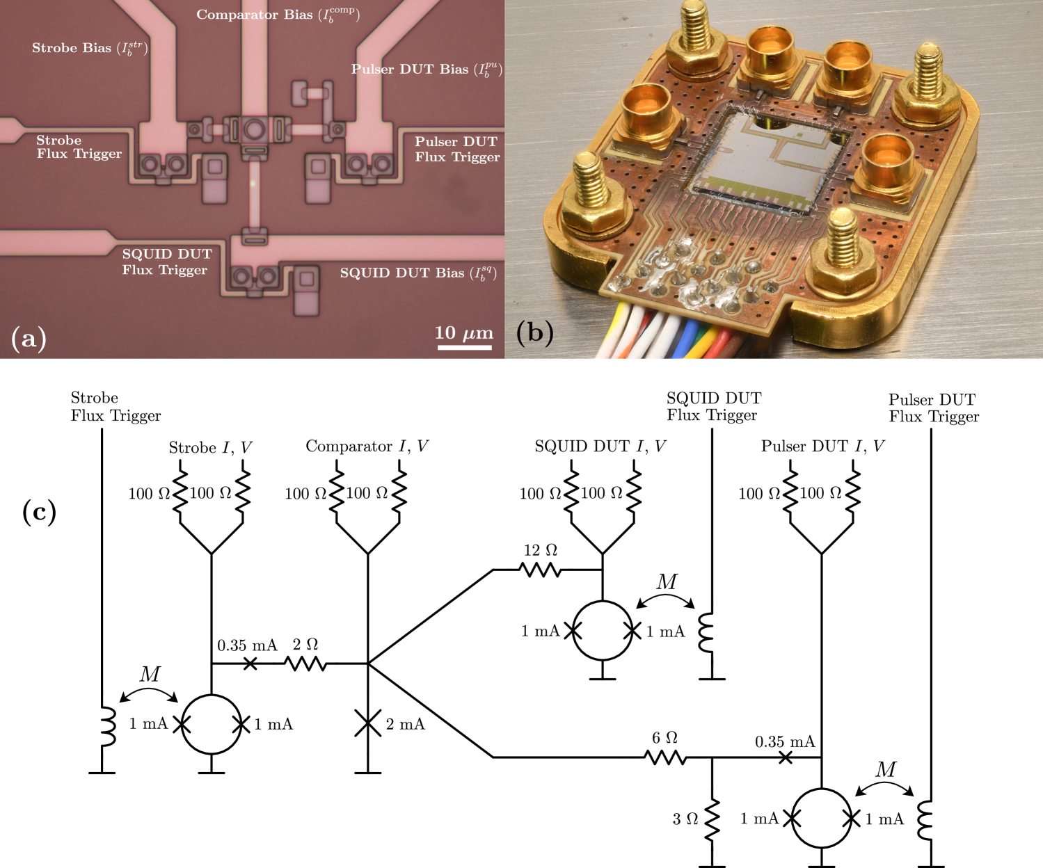
As a launching point for developing a flexible JJ sampler technology for waveform metrology and diagnostics of SFQ digital logic circuits, we fabricated a sampler using unshunted amorphous silicon barrier (Nb/a-Si/Nb) JJs with a critical current density of mA/m2. The fabricated circuit is shown in Fig 7(a) and the packaged 1 cm1 cm chip is shown in Fig 7(b). We select this junction technology due to its potential to scale to significantly higher , a critical parameter in increasing latching junction operating speed Harris (1979); Van Zeghbroeck (2024), when compared to more common Nb/Al-AlOx/Nb JJs Olaya et al. (2023a); Tolpygo et al. (2017).
The chosen topology is shown in Fig 7(c) and is similar to [(15)]. The sampler circuit is comprised of four primary components: the comparator ( mA), a strobe pulse generator, a step signal DUT, and an impulse generator DUT. The strobe pulse and impulse generator DUT are realized using Faris pulsers Faris (1980), consisting of a two-junction, symmetric dc SQUID (single junction mA), and a smaller output pulser junction with A. The SQUIDs comprising the Faris pulsers are identical to the SQUID DUT. The strobe and DUT signals are triggered using fast current pulses carried to the sampler circuit on high-bandwidth lines (coaxial cables off-chip, CPW on-chip). Further fabrication details may be found in Appendix C. Including all coupling resistors (), and using fabrication parameters stated in Sec. III, we obtain an expected comparator for the fabricated devices.
The sampler die is soldered using 52In/48Sn solder Howe et al. (2012); Schwall et al. (2011); Chong, Dresselhaus, and Benz (2003) inside a copper enclosure which is mounted on the second stage of a Gifford-McMahon-cooled cryostat and operated at 3.6 K. The device package possesses four high speed lines, used for applying flux trigger pulses, and 14 low-speed current bias and voltage tap leads. High speed lines exit the package via SMP connectors and are converted to SMA-connectorized semi-flex and rigid coaxial cables. We thermalize the flux trigger lines using 10 dB attenuators at 3.6 K. All low-speed lines are combined in a multi-wire cryogenic loom and are thermalized with two sets of 100 series resistors at 3.6 K. Additionally a set of on-chip 100 series resistors are fabricated as a final thermalization step and to create a stiff current bias in proximity to the sampler subcircuits.
Our choice of Nb/a-Si/Nb JJs permits operation over a wide temperature range thanks to the temperature-insensitivity of for this JJ technology – which is reduced to half its asymptotic low-temperature value (i.e. below 4 K) at around 7 K Howe et al. (2022); Olaya et al. (2023a). Power dissipation () becomes the primary consideration for sampler operation in terms of the low-temperature bound and limits operation of samplers using JJs with an of order 1 mA to around 1 K. Samplers using lower JJs may easily be constructed to permit operation at dilution refrigerator temperatures Leonard et al. (2019); Di Marino et al. (2024); Yohannes et al. (2023).
IV.2 Experimental Setup
We apply current biases using a series of low-speed (1 GSa/s) AWGs configured to output square voltage pulses at a frequency of 20 kHz, with edge times of 30 s, and a duty cycle of 0.8. The strobe and DUT flux triggers are supplied using step function voltage pulses from a multichannel, high-speed AWG (65 GSa/s, 25 GHz analog bandwidth). Discarding the bandwidth limit of cabling and interconnects, this means the trigger pulse rise time is of order 15 ps. Delay (advancement) of the firing time of the DUT relative to the strobe is accomplished by applying a negative (positive) dc level to the flux trigger by means of a dc voltage source, bias tee, and mechanical phase shifter (delay line) Wolf, Van Zeghbroeck, and Deutsch (1985). In our case we apply flux offsets to advance the DUT while the strobe trigger time is held constant. As a dc flux bias reduces the critical current of the SQUIDs in the DUTs and strobe, this technique is limited in the maximum strobe-DUT traversal of approximately 30–100 ps; depending on the proximity of to (less traversal is possible the higher the DUT bias). For timing calibration and system tuneup we operate the strobe and DUT triggers on independent channels, allowing us to program arbitrary strobe-DUT delays and determine optimal alignment parameters for the flux trigger waveform data. In this configuration we treat the flux trigger AWG sample clock as a master timing reference and perform a delay calibration of the mechanical delay line. Next, and to eliminate channel-to-channel jitter, we move to single output configuration where the strobe and DUT flux triggers are split with a power divider at the AWG output (with the bias tee and delay line following the divider for the DUT trigger line).
Rather than adopt the analog approach of historical JJ sampler demonstrations using a slow feedback loop, we implement a fully digital system for acquiring DUT waveforms using our sampler device. The comparator voltage is captured on a 125 MSa/s digitizer and we implement the same binary search algorithm used in our simulations Van Zeghbroeck, Howe, and Hopkins (2024). The data from the full sampling period is post-processed to select the trace segment known to follow the arrival of the flux triggers, and use this voltage to determine if the comparator has switched for a given bias. Implementation of the binary search is thus straightforward with the single caveat that, in the presence of noise, we must collect multiple sampling events and enforce a switching probability threshold for each programmed strobe-signal delay (dc flux offset). Empirically, we find 1000 sampling events and a switching probability threshold of 0.5 to provide high-quality, repeatable sampled waveforms. With these settings and 10 binary search steps, the acquisition time is s per commanded delay – limited by data transfer and post-processing. The advantage of this technique is that it directly mirrors the sampling process as performed in simulation, facilitating strong agreement between simulated and measured results.
IV.3 Sampled Waveforms: DUT Current Bias Sweep
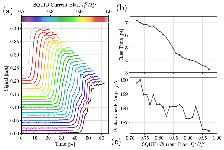
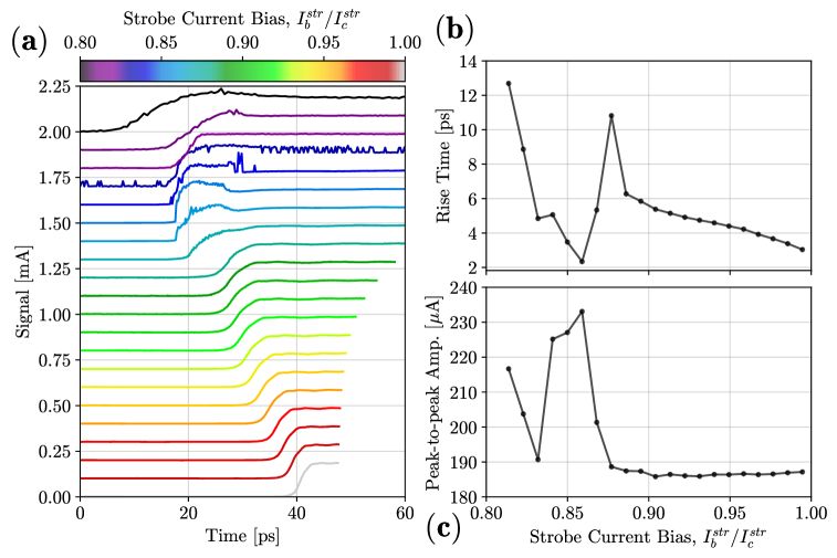
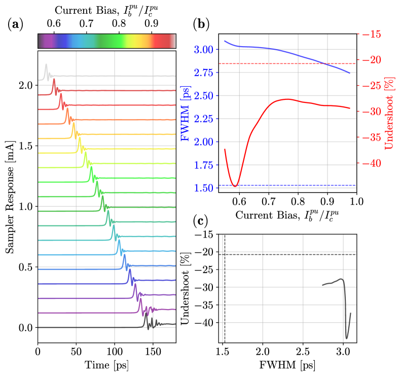
After initial tune-up and dc characterization of the device subcircuits (Appendix B), we perform a series of sweeps to fully explore the sampler and DUT dynamics. We begin by selecting a fixed strobe current bias of 2.2 mA; close to its practical maximum of mA to provide the sharpest strobe pulse Donnelly et al. (2020); Van Zeghbroeck (2024). Noise- and thermal-oscillation-induced spurious switching is not present in our sampler even with the strobe bias this close to its critical current via sufficient filtering of the bias lines and the negligible temperature sensitivity of Nb/a-Si/Nb at 3.6 K Olaya et al. (2023a). We then sample the SQUID DUT waveform for a variety of DUT current biases. All of the sampler measurements presented in Fig. 8 and Fig. 10 were collected by advancing the DUT relative to the strobe.
Calibration of the delay as a function of the flux trigger offset voltage (i.e. in ps/V corresponding to the signal advancement as depicted in Fig. 1(b)) is performed as in [(15)] using a mechanical delay line (phase shifter). This procedure involves sampling the DUT (at fixed current bias) waveform at two different delay line settings and measuring the separation between the curves, in flux offset voltage units, corresponding to the known delay induced by the two shifter positions. Using this technique the delay, per volt applied as a flux offset, may be known to sub-picosecond levels. This delay calibration is linear and reproducible with respect to the full range of applied DUT trigger dc flux offsets used to gather the sampled waveforms shown in Fig. 8 and Fig. 10. We obtain a constant value of 17.8 ps/V using a 1 k current-defining resistor. See Fig. 16 in the appendix for more details.
In Fig. 8 and Fig. 10, the sampled waveforms each have approximately 600 points over a span of 40–60 ps. At each point the sampler performs a binary search depth of 10, where each binary step consists of comparator decisions, for a total of comparator decisions made for each signal data point. The full scale search range selected for these signal data was 300 A, which gives a current resolution of nA. To characterize repeatability and uncertainty of these measurements, we sampled and recorded several complete signal waveforms with identical settings for all control parameters. At each programmed delay we calculate the Type A uncertainty Possolo (2015) for the signal values. On the steepest regions of the curves corresponding to the largest uncertainty, we determine the DUT current Type A uncertainty for a 95% confidence interval () of 1.2 A (). This is a relative uncertainty of in Fig. 8 and in Fig. 10. The error in the commanded delay arises from the uncertainty in the delay-to-dc-flux-offset calibration applied to the DUT flux trigger line. These uncertainties result in an expansion or compression of the waveforms by less than 0.3%.
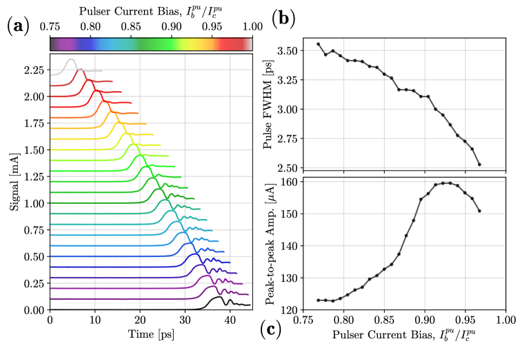
The family of sampled waveforms for the latching SQUID are shown in Fig 8. At low DUT bias the sampled waveform shows two “bumps” in the rising edge of the step waveform that disappear with increasing . Fast oscillations near the top of the rising edge also disappear and are replaced with slower oscillations. We may quantify the frequency of these oscillations by performing a polynomial and sinusoidal fit to the signal above its 90% threshold via
| (1) |
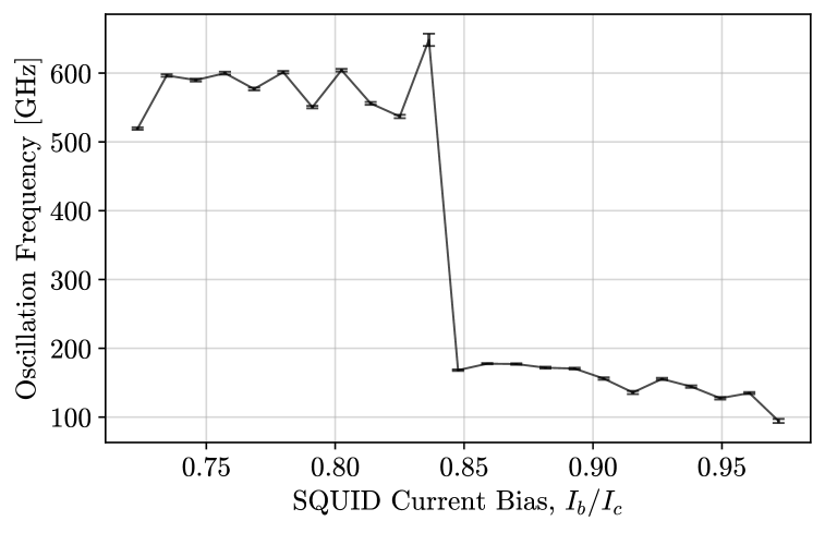
Fig. 9 shows the behavior of the SQUID DUT’s oscillations as a function of its current bias. From this we see the comparator responds to oscillating signals with periods shorter than the extracted rise time of ps; demonstrating our sampler is sensitive to signals in excess of 600 GHz. In this case, the measured value of the sampler is in fact partially limited by the SQUID DUT dynamics and its intrinsic rise time (as discussed in Sec. III.1.1).
These results, notably for DUT current biases of are in good agreement with oscillations sampled in [(15)]. The physical dynamics giving rise to the two oscillation frequencies arise from the small delay in latching time of each of the SQUID junctions – which in turn is a function of the SQUID bias and decreases as the bias increases (see Appendix G). This time delay, ranging from 1.1 ps to 0.7 ps (from low to high bias), causes an appreciable beat oscillation between each SQUID JJ, which is detectable by our sampler even though this frequency is above the sampler bandwidth as extracted using a linear systems treatment. At high bias, the observed oscillations are reduced in frequency and are due to intrinsic oscillations of the underdamped comparator.
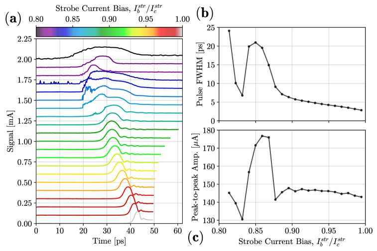
Next we perform the same measurement as above, but this time with the Faris pulser DUT. The strobe bias is again held at 2.2 mA and we sample the pulser DUT signal as a function of its bias current . These results, in tandem with the fast oscillations shown in Fig. 8(a), demonstrate the intrinsic response time of the sampler is actually faster than what is extracted via the 10%–90% rise time while sampling the SQUID DUT. Again we observe features on faster timescales than the minimum shown in Fig. 8(b) and whose dynamics change as a function of the impulse DUT bias – demonstrating they are sourced by the DUT and are not resulting from the convolution of the comparator dynamics. This is further evidenced by the fact the measured pulser DUT amplitude increases, reaches a measured maximum, and then begins to decrease – while the FWHM monotonically decreases with increasing . Similar to the variation in the sampled oscillation for the step signal DUT, the reduction in FWHM is the result of a reduction in the time delay between the switching of the two JJs comprising the SQUID of the Faris pulser. As the time between each JJ switching event is minimized, the pulse amplitude is expected to monotonically increase. Our observation of a maximum pulse amplitude at , corresponding to a DUT FWHM of 2.8 ps, shows this is the regime where the intrinsic speed of the comparator is exceeded by the speed of the pulser DUT signal. Beyond this point the reduction in the sampled DUT FWHM is expected as, at this point, the sampler has entered the regime of a bandwidth-limited detector.
V Sampler Bandwidth
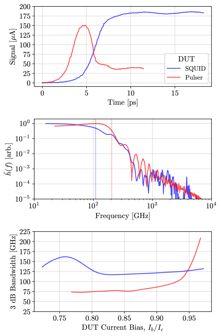
The 3 dB bandwidth, , of the sampler may be approximated using the measurements in the previous section by treating the sampler as a first-order linear system Åström and Murray (2007). We perform this analysis on the data in Fig. 8 and Fig. 10 where the strobe current bias is held fixed as each DUT current bias is swept. To extract we compute the transfer function corresponding to each and trace by Fourier transforming the sampled response and locating the point where the transfer function drops by 3 dB from its dc value. In our case, we choose the dc value to be the lowest frequency in the transfer function. Due to the steep rolloff in the transfer function no windowing is necessary to suppress ringing at high frequencies. As the SQUID DUT traces are of non-uniform length the data must be zero-padded so each record has a length equal to the longest un-padded trace. Additionally, because the transfer function applies only to periodic (or finite-duration) pulses, we differentiate the SQUID DUT data after zero-padding. Neither procedure is needed for the pulser DUT bandwidth extraction Åström and Murray (2007).
Fig. 11 shows the results of this analysis. Note that, because the DUT signals are not infinitely sharp, these measurements extract the convolution, , of the DUT signal with the sampler’s true transfer function, . We observe that is clearly not saturating at the highest DUT biases (narrowest pulses and fastest rise time step signals), which demonstrates a lower bound of 175 GHz for the intrinsic sampler bandwidth. This agrees well with the fitted oscillation frequencies in the sampler reconstruction of the SQUID DUT waveforms as a function of DUT bias (Fig. 8) and, were it possible to realize a sharper Faris pulser DUT pulse, would be expected to display a rolloff near 600 GHz. While it is true that the system dynamics are still increasing even at the highest DUT biases measured, it is not possible to further increase the bias and still fully sample the target waveform. This is because the dc flux offset delay technique also reduces the DUT critical current and, for a given , this sets a limit on how much the DUT may be advanced before it latches during the set bias phase of the sampling period.
VI Conclusions
We have performed detailed simulations using a novel binary search threshold detection algorithm to understand the critical design criteria for optimizing the performance of a JJ-based sampler realized via a single latching comparator junction and two galvanically-connected DUTs: a latching SQUID and Faris pulser. The JJ parameters chosen in simulation closely match those observed using NIST’s 0.2 mA/m2 Nb/a-Si/Nb JJ process Olaya et al. (2023a). Using the latching SQUID DUT to provide a step signal we establish bounds on the expected intrinsic sampler rise time to be approximately 2.4–3.4 ps. With the Faris pulser we find the minimum pulse FWHM the sampler can resolve is 2.5–3.0 ps. Via full simulation of the sampling process we reveal a tradeoff between a small increase in the sampler speed at the expense of significant (10% peak signal amplitude) distortion when pushing to the lower limit of (FWHM) by increasing the comparator . Exploration of the relative coupling strengths of the strobe pulse and DUT signal, , showed a relative narrow optimum range of . In these simulations we note that the fastest response (minimum and FWHM) is, in some cases, limited by the DUT dynamics and not those of the comparator. Using a SQUID DUT model optimized to provide a 0.47 ps 10%–90% rise time, we demonstrate the comparator speed limit is actually expected to be 1.9 ps for the 0.2 mA/m2 process. We also simulated capacitive and inductive DUT-comparator coupling schemes (Appendix D) to determine upper bounds on the coupler capacitance and inductance below which the sampler performance (bandwidth, signal distortion) is not significantly compromised.
As an experimental realization of JJ sampler technology, we have designed and fabricated a latching Josephson sampler galvanically-connected to two DUTs using our modern JJ tri-layer process with niobium electrodes and amorphous silicon barriers (Nb/a-Si/Nb). Waveforms of both DUTs were experimentally measured at 3.6 K using the same binary search technique employed in simulation, each as a function of DUT and strobe bias. Our experimental results are in good agreement with simulation and showed the fastest response corresponding to a rise time and FWHM of 3.3 ps and 2.5 ps when measuring the SQUID and Faris pulser DUTs, respectively. These values correspond to the rise time and FWHM for sampled waveforms with the sampler operating in a distortion-minimizing state (high strobe bias, see Appendix E). A linear-systems analysis of the sampled SQUID and pulser waveforms yield a sampler bandwidth of 160 GHz and 210 GHz, respectively. However, we measure oscillatory signals above 600 GHz which transition to a lower frequency as DUT bias is increased. This dependence on DUT bias indicates the oscillations source from the DUT itself and are thus a real component of the signal rather than an artifact of the comparator dynamics convolved with the true signal. Observation of these high frequency signals both supports the assertion that our characterization of the intrinsic sampler speed limit is limited by the DUT circuits, not the comparator, and demonstrates potential bandwidth capabilities well beyond the previous best-in-field demonstrations. This simulation framework and laboratory demonstration provides a concrete path forward for ultra-fast and high-precision on-chip waveform metrology for superconducting electronics.
Acknowledgements.
L. Howe thanks M. Castellanos-Beltran for numerous fruitful discussions lending greatly to the success of this work. This work is a contribution of the U.S. government and is not subject to U.S. copyright.Data Availability Statement
The data that support the findings of this study are openly available in Josephson Samplers: Optimal Design and Demonstration at https://datapub.nist.gov/od/id/mds2-3649, with DOI doi:10.18434/mds2-3649.
References
- Rüfenacht, Flowers-Jacobs, and Benz (2018) A. Rüfenacht, N. E. Flowers-Jacobs, and S. P. Benz, “Impact of the latest generation of Josephson voltage standards in ac and dc electric metrology,” Metrologia 55, S152 (2018).
- Bauer et al. (2022) S. Bauer, R. Behr, J. Herick, O. Kieler, M. Kraus, H. Tian, Y. Pimsut, and L. Palafox, “Josephson voltage standards as toolkit for precision metrological applications at PTB,” Measurement Science and Technology 34, 032001 (2022).
- Castellanos-Beltran and Lehnert (2007) M. Castellanos-Beltran and K. Lehnert, “Widely tunable parametric amplifier based on a superconducting quantum interference device array resonator,” Applied Physics Letters 91, 083509 (2007).
- Roy and Devoret (2018) A. Roy and M. Devoret, “Quantum-limited parametric amplification with Josephson circuits in the regime of pump depletion,” Physical Review B 98, 045405 (2018).
- Macklin et al. (2015) C. Macklin, K. O’brien, D. Hover, M. Schwartz, V. Bolkhovsky, X. Zhang, W. Oliver, and I. Siddiqi, “A near–quantum-limited Josephson traveling-wave parametric amplifier,” Science 350, 307–310 (2015).
- Fourie (2018) C. J. Fourie, “Digital superconducting electronics design tools—Status and roadmap,” IEEE Transactions on Applied Superconductivity 28, 1300412 (2018).
- Fourie et al. (2019) C. J. Fourie, K. Jackman, M. M. Botha, S. Razmkhah, P. Febvre, C. L. Ayala, Q. Xu, N. Yoshikawa, E. Patrick, M. Law, et al., “ColdFlux superconducting EDA and TCAD tools project: Overview and progress,” IEEE Transactions on Applied Superconductivity 29, 1300407 (2019).
- Blais et al. (2021) A. Blais, A. L. Grimsmo, S. M. Girvin, and A. Wallraff, “Circuit quantum electrodynamics,” Reviews of Modern Physics 93, 025005 (2021).
- Krantz et al. (2019) P. Krantz, M. Kjaergaard, F. Yan, T. P. Orlando, S. Gustavsson, and W. D. Oliver, “A quantum engineer’s guide to superconducting qubits,” Applied Physics Reviews 6, 021318 (2019).
- Leonard et al. (2019) E. Leonard, M. A. Beck, J. Nelson, B. Christensen, T. Thorbeck, C. Howington, A. Opremcak, I. Pechenezhskiy, K. Dodge, N. Dupuis, M. Hutchings, J. Ku, F. Schlenker, J. Suttle, C. Wilen, S. Zhu, M. Vavilov, B. Plourde, and R. McDermott, “Digital Coherent Control of a Superconducting Qubit,” Phys. Rev. Appl. 11, 014009 (2019).
- Howe et al. (2022) L. Howe, M. A. Castellanos-Beltran, A. J. Sirois, D. Olaya, J. Biesecker, P. D. Dresselhaus, S. P. Benz, and P. F. Hopkins, “Digital Control of a Superconducting Qubit Using a Josephson Pulse Generator at 3 K,” PRX Quantum 3, 010350 (2022).
- Castellanos-Beltran et al. (2023) M. Castellanos-Beltran, A. Sirois, L. Howe, D. Olaya, J. Biesecker, S. P. Benz, and P. Hopkins, “Coherence-limited digital control of a superconducting qubit using a Josephson pulse generator at 3 K,” Applied Physics Letters 122, 192602 (2023).
- Ketchen, Herrell, and Anderson (1985) M. Ketchen, D. Herrell, and C. Anderson, “Josephson cross-sectional model experiment,” Journal of Applied Physics 57, 2550–2574 (1985).
- Hamilton (1979) C. A. Hamilton, U.S. Patent No. 4245169 (14 Mar 1979).
- Wolf, Van Zeghbroeck, and Deutsch (1985) P. Wolf, B. Van Zeghbroeck, and U. Deutsch, “A Josephson sampler with 2.1 ps resolution,” IEEE Transactions on Magnetics 21, 226–229 (1985).
- Van Zeghbroeck (1985) B. Van Zeghbroeck, “Model for a Josephson sampling gate,” Journal of Applied Physics 57, 2593–2596 (1985).
- Faris (1979) S. M. Faris, U.S. Patent No. 4401900 (20 Dec 1979).
- Kolner and Bloom (1986) B. Kolner and D. Bloom, “Electrooptic sampling in GaAs integrated circuits,” IEEE Journal of quantum electronics 22, 79–93 (1986).
- Seitz et al. (2006) S. Seitz, M. Bieler, G. Hein, K. Pierz, U. Siegner, F. Schmückle, and W. Heinrich, “Characterization of an external electro-optic sampling probe: Influence of probe height on distortion of measured voltage pulses,” Journal of Applied Physics 100, 113124 (2006).
- Wang et al. (1995) C.-C. Wang, M. Currie, D. Jacobs-Perkins, M. J. Feldman, R. Sobolewski, and T. Y. Hsiang, “Optoelectronic generation and detection of single-flux-quantum pulses,” Applied Physics Letters 66, 3325–3327 (1995).
- Hegmann et al. (1995) F. Hegmann, D. Jacobs-Perkins, C.-C. Wang, S. Moffat, R. Hughes, J. Preston, M. Currie, P. Fauchet, T. Hsiang, and R. Sobolewski, “Electro-optic sampling of 1.5-ps photoresponse signal from YBa2Cu3O7- thin films,” Applied Physics Letters 67, 285–287 (1995).
- Keil and Dykaar (1992) U. Keil and D. Dykaar, “Electro-optic sampling and carrier dynamics at zero propagation distance,” Applied Physics Letters 61, 1504–1506 (1992).
- Tuckerman (1980) D. B. Tuckerman, “A Josephson ultrahigh-resolution sampling system,” Applied Physics Letters 36, 1008–1010 (1980).
- Faris (1980) S. M. Faris, “Generation and measurement of ultrashort current pulses with Josephson devices,” Applied Physics Letters 36, 1005–1007 (1980).
- Whiteley et al. (1988) S. Whiteley, E. Hanson, G. Hohenwarter, F. Kuo, and S. Faris, “Technologies for a superconducting sampling oscilloscope/time domain reflectometer,” Proceedings, Interconnection of High Speed and High Frequency Devices and Systems 0947, 138–145 (SPIE,1988).
- Akoh et al. (1983) H. Akoh, S. Sakai, A. Yagi, and H. Hayakawa, “A direct coupled Josephson sampler,” Japanese Journal of Applied Physics 22, L435 (1983).
- Akoh et al. (1985) H. Akoh, S. Sakai, A. Yagi, and H. Hayakawa, “Real time fluxon dynamics in Josephson transmission line,” IEEE Transactions on Magnetics 21, 737–740 (1985).
- Sakai, Akoh, and Hayakawa (1983) S. Sakai, H. Akoh, and H. Hayakawa, “Fluxon observation using a Josephson sampler,” Japanese Journal of Applied Physics 22, L479 (1983).
- Harris, Wolf, and Moore (1982) R. E. Harris, P. Wolf, and D. Moore, “Electronically adjustable delay for Josephson technology,” IEEE Electron Device Letters 3, 261–263 (1982).
- Whiteley (1988) S. Whiteley, U.S. Patent No. 4789794 (26 Sep 1986); U.S. Patent No. 4866302 (7 July 1988).
- Andrews (1989) J. R. Andrews, “Comparison of Ultra-Fast Rise Sampling Oscilloscopes,” Picosecond Pulse Labs Application Note AN-2a (Feb 1989).
- Maruyama et al. (2005) M. Maruyama, H. Suzuki, T. Hato, H. Wakana, K. Nakayama, Y. Ishimaru, O. Horibe, S. Adachi, A. Kamitani, K. Suzuki, et al., “Observation of 45 GHz current waveforms using HTS sampler,” Physica C: Superconductivity and its applications 426, 1661–1667 (2005).
- Hidaka et al. (1999) M. Hidaka, T. Satoh, M. Koike, and S. Tahara, “High-resolution measurement by a high-Tc superconductor sampler,” IEEE Transactions on Applied Superconductivity 9, 4081–4086 (1999).
- Suzuki et al. (2005) H. Suzuki, T. Hato, M. Maruyama, H. Wakana, K. Nakayama, Y. Ishimaru, O. Horibe, S. Adachi, A. Kamitani, K. Suzuki, et al., “Progress in HTS sampler development,” Physica C: Superconductivity and its applications 426, 1643–1649 (2005).
- Maruyama et al. (2007) M. Maruyama, H. Wakana, T. Hato, H. Suzuki, K. Tanabe, K. Uekusa, T. Konno, N. Sato, and M. Kawabata, “Observation of SFQ pulse using HTS sampler,” Physica C: Superconductivity and its applications 463, 1101–1105 (2007).
- Olaya et al. (2023a) D. I. Olaya, J. Biesecker, M. A. Castellanos-Beltran, A. J. Sirois, P. F. Hopkins, P. D. Dresselhaus, and S. P. Benz, “Nb/a-Si/Nb Josephson junctions for high-density superconducting circuits,” Applied Physics Letters 122, 182601 (2023a).
- Olaya et al. (2023b) D. Olaya, J. Biesecker, M. Castellanos-Beltran, A. Sirois, L. Howe, P. Dresselhaus, S. Benz, and P. Hopkins, “Nb/a-Si/Nb-Junction Josephson Arbitrary Waveform Synthesizers for Quantum Information,” IEEE Transactions on Applied Superconductivity 33, 1400205 (2023b).
- Askerzade (2006) I. Askerzade, “Josephson-effect samplers: A review,” Technical physics 51, 393–400 (2006).
- Van Zeghbroeck, Howe, and Hopkins (2024) B. J. Van Zeghbroeck, L. Howe, and P. F. Hopkins, “Josephson Sampler Response using a Binary Search Algorithm,” IEEE Transactions on Applied Superconductivity 34, 1701206 (2024).
- Van Zeghbroeck (2024) B. J. Van Zeghbroeck, “Switching Time Versus DC Current Overdrive of a Josephson Junction Sampler,” IEEE Transactions on Applied Superconductivity 34, 1101604 (2024).
- Åström and Murray (2007) K. J. Åström and R. M. Murray, Feedback systems:An Introduction for Scientists and Engineers (Princeton University Press, 2007) pp. 27–64.
- (42) Commercial instruments and software are identified in this paper in order to adequately specify the experimental procedure. Such identification does not imply recommendation or endorsement by NIST, nor does it imply that the product identified is necessarily the best available for the purpose.
- (43) Whiteley Research Inc., WRspice (v4.3.17): IC design sofware for Linux, OSX, and Windows.
- (44) Whiteley Research Inc., XicTools (v4.3.17) source code repository.
- Olaya et al. (2019) D. Olaya, M. Castellanos-Beltran, J. Pulecio, J. Biesecker, S. Khadem, T. Lewitt, P. Hopkins, P. Dresselhaus, and S. Benz, “Planarized process for single-flux-quantum circuits with self-shunted Nb/NbxSi1-x /Nb Josephson junctions,” IEEE Transactions on Applied Superconductivity 29, 1101708 (2019).
- Cui et al. (2017) Z. Cui, J. R. Kirtley, Y. Wang, P. A. Kratz, A. J. Rosenberg, C. A. Watson, G. W. Gibson, M. B. Ketchen, K. Moler, et al., “Scanning SQUID sampler with 40-ps time resolution,” Review of Scientific Instruments 88, 083703 (2017).
- Harris (1979) E. Harris, “Turn-on delay of Josephson interferometer logic devices,” IEEE Transactions on Magnetics 15, 562–565 (1979).
- Whiteley et al. (2023) S. Whiteley, A. Barker, E. Mlinar, J. Kawa, S. S. Meher, J. Ravi, and A. Inamdar, “Observations in Use of a Tunnel Junction Model in Simulations of Josephson Digital Circuits,” IEEE Transactions on Applied Superconductivity 33, 1300509 (2023).
- Tolpygo et al. (2017) S. K. Tolpygo, V. Bolkhovsky, S. Zarr, T. J. Weir, A. Wynn, A. L. Day, L. M. Johnson, and M. A. Gouker, “Properties of Unshunted and Resistively Shunted Nb/AlOx-Al/Nb Josephson Junctions With Critical Current Densities From 0.1 to 1 mA/m2,” IEEE Transactions on Applied Superconductivity 27, 1100815 (2017).
- Howe et al. (2012) L. Howe, C. J. Burroughs, P. D. Dresselhaus, S. P. Benz, and R. E. Schwall, “Cryogen-free operation of 10 V programmable Josephson voltage standards,” IEEE transactions on applied superconductivity 23, 1300605–1300605 (2012).
- Schwall et al. (2011) R. E. Schwall, D. Zilz, J. Power, C. J. Burroughs, P. D. Dresselhaus, and S. P. Benz, “Practical operation of cryogen-free programmable Josephson voltage standards,” IEEE transactions on applied superconductivity 21, 891–895 (2011).
- Chong, Dresselhaus, and Benz (2003) Y. Chong, P. Dresselhaus, and S. Benz, “Thermal transport in stacked superconductor–normal metal–superconductor Josephson junctions,” Applied physics letters 83, 1794–1796 (2003).
- Di Marino et al. (2024) L. Di Marino, L. Di Palma, M. Riccio, M. Arzeo, and O. Mukhanov, “Control of a Josephson Digital Phase Detector via an SFQ-based Flux Bias Driver,” arXiv preprint arXiv:2412.11961 (2024).
- Yohannes et al. (2023) D. Yohannes, M. Renzullo, J. Vivalda, A. Jacobs, M. Yu, J. Walter, A. Kirichenko, I. Vernik, and O. Mukhanov, “High density fabrication process for single flux quantum circuits,” Applied Physics Letters 122 (2023).
- Donnelly et al. (2020) C. A. Donnelly, N. E. Flowers-Jacobs, J. A. Brevik, A. E. Fox, P. D. Dresselhaus, P. F. Hopkins, and S. P. Benz, “1 GHz Waveform Synthesis With Josephson Junction Arrays,” IEEE Transactions on Applied Superconductivity 30, 1400111 (2020).
- Possolo (2015) A. Possolo, “Nist technical note 1900: Simple guide for evaluating and expressing the uncertainty of nist measurement results,” Tech. Rep. (NIST, 2015).
Picosecond Josephson Samplers: Modeling and Measurements – Supplemental Information
Appendix A Binary Search Algorithm and Implementation
The binary search algorithm Van Zeghbroeck, Howe, and Hopkins (2024) starts with the selection of a minimum and maximum bias current that will be applied to the comparator. These are to be chosen such that the range of amplitudes in the signal of interest is smaller than the difference between those two currents and with an appropriate offset to avoid clipping of the response. Properly chosen, the max (min) biases will result in the comparator always (never) latching for all delays – i.e for all delays which align the strobe to sample any portion of the signal.
First, two initial simulations are run with and to guarantee the maximum and minimum biases are appropriately chosen. We then define, for iteration number ,
| (2) |
| (3) |
| (4) |
set the bias for the first binary search step to
| (5) |
and determine if the junction latches under this dc bias (a “1") or not (a “0"). If the result of simulation was a 1 we select the lower bias midpoint by setting
| (6) |
| (7) |
and conversely for simulation yielding the 0 result we select the upper midpoint:
| (8) |
| (9) |
Thus, the bias at simulation step is
| (10) |
We implement this technique in simulation using WRspice NIS ; wrs . To simulate a full sampling reconstruction of the target waveform with respect to a given circuit parameter, we simulate only single sampling periods at a time, of duration 200–1200 ps depending on the parameter sweep being run, and adjust only the comparator bias or signal trigger delay. We first fix the signal trigger delay and perform a binary search to determine the new value at which results in latching of the comparator. Latching of the comparator is determined when the mean voltage over a fixed time window exceeds a threshold (typically the gap voltage). The number of steps in the binary search is chosen to yield an resolution of nA. Next the signal trigger delay is adjusted, we repeat the search, and iterate until the entire target waveform is sampled. Finally, to characterize the response of the full sampler output with respect to a given circuit parameter, we adjust this parameter and repeat the full sampling operation described above.
Simulations of the sampling process using the binary search are significantly faster than simulations that implement the slow (of order 10–100 Hz) feedback circuit method used in the experiments by (15). The speedup can be as large as a factor of or more. Furthermore, our binary search simulation strategy yields high-resolution ( nA, ps) simulations of complete target waveforms in minutes Van Zeghbroeck, Howe, and Hopkins (2024).
Appendix B DC Subcircuit Characterization
As shown in in the circuit diagram of Fig. 7(c), the designed sampler has current and voltage taps for each subcircuit on the sampler die (comparator, strobe, SQUID DUT, and pulser DUT). This feature allows us to easily characterize each individual component of the sampler via - and vs. curves. One such curve for the strobe generator is shown in Fig. 12 where a dc flux is applied via the strobe’s high speed flux trigger line, and the bias current is then ramped up and down from zero to measure . We repeat these measurements for the comparator (only an - curve as there is no flux control of the comparator), SQUID, and Faris pulser DUTs to determine appropriate bias currents and flux pulse amplitudes. Note that the effect of applying a flux pulse to trigger waveform emission is to traverse the critical current in the vertical direction in Fig. 12.
As an additional characterization we confirm the design of the SQUIDs internal to all on-chip signal generators by measuring the screening parameter and extracting the SQUID loop inductance. The SQUID screening parameter is estimated Van Zeghbroeck, Howe, and Hopkins (2024) by ramping the dc flux bias through the flux trigger line while measuring the SQUID critical current, and using
| (11) |
We obtain and a total SQUID loop inductance of pH. Electromagnetic simulations estimated this value to be pH and we attribute this discrepancy to the apodization near the SQUID loop pinhole during photolithography – resulting in a smaller open area than was designed. The designed geometry was a m square, which is near the minimum feature size for optical lithography in our fabrication process. From the micrograph in Fig. 7(a) we obtain a geometry closer to m m which can explain a lower screening parameter as a smaller effective SQUID loop lowers .
Appendix C Device Fabrication
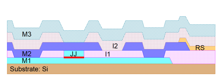
The fabrication process for the sampler circuits, shown in Fig. 13, is based on the process for SFQ circuits developed at NIST and described in [(45)], with a few modifications. In this case, the substrate was 76 mm intrinsic silicon with no thermal oxide. Three superconducting Nb layers were used, M1 to M3 from bottom to top, all deposited by dc sputtering and patterned by reactive ion etching using sulfur hexafluoride gas. The junction barrier was sputtered amorphous silicon, deposited in situ with the base electrode (M1) and junction counter electrode (M2). The barrier thickness was chosen to obtain a junction critical current density of 0.2 mA/m2. The insulating layers, consisting of silicon oxide, were deposited by electron cyclotron resonance plasma enhanced chemical vapor deposition (ECR-PECVD). Only one planarization step, on insulator layer I1, was done. The resistors, of palladium gold alloy and defined by lift-off, were deposited on top of M2 layer, as shown in the schematic.
Appendix D Reactive Coupling Simulations – Detailed Results
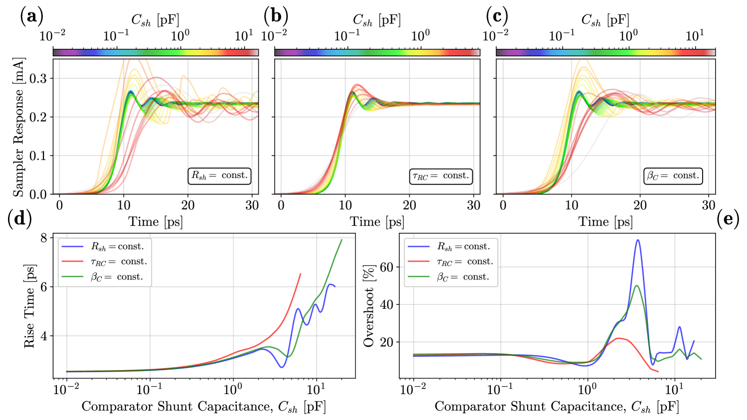
In some instances a galvanic comparator-DUT coupling may be undesirable, e.g. in the event a scanning sampler is the preferred system Cui et al. (2017). For the topology of Fig. 2, reactive coupling may be achieved either by a capacitance in parallel (shunt), , with the comparator junction, or with an inductance in series, . First we examine the case of a parallel capacitive coupling by performing a simulation while sweeping . To keep the DUT output signal constant during the simulation, the galvanic connection was kept () in order to enforce a fixed strobe-to-signal ratio and avoid any complications detailed in the results of Fig. 4. Note that in a true capacitively-coupled sampler the circuit topology would be the same as in Fig. 2 except that would be replaced by a coupling capacitor ; in this case the equivalent shunt capacitance of the comparator is (in this simplified simulation we ignored the capacitance to ground in the DUT). For typical coupling capacitances of pF and voltage slew rates of mV/ps, the peak current through the capacitor is mA – demonstrating signals with sufficient amplitudes may be applied to the comparator via capacitive couplers.
The coupling capacitance is expected to have negligible effect on the sampler operation in the regime pF. In these simulations, however, once approaches the comparator junction capacitance it perturbs both the comparator Stewart-McCumber parameter and the time constant . As we anticipate requiring couplers with close to 1 pF of capacitance we explore two options to compensate for these effects: (i) adjust the explicit shunt resistance to keep constant, and (ii) adjust to keep constant – as well as the case where no compensation is performed. In both cases must be reduced as increases so we begin these simulations with a negligible pF and (baseline ) to permit compensation over the widest range of while maintaining an underdamped comparator. Fig. 14 shows the results of these simulations and, as expected, little impact is seen for pF. For above 1 pF both the uncompensated and constant- case show adverse distortion relative to the constant- case but do yield small gains in preserving the low- rise time compared to the constant- results. Nevertheless, all three parameter sweeps clearly demonstrate that, for optimal performance in a capacitively-coupled device, care must be taken to ensure the comparator junction capacitance is dominant.
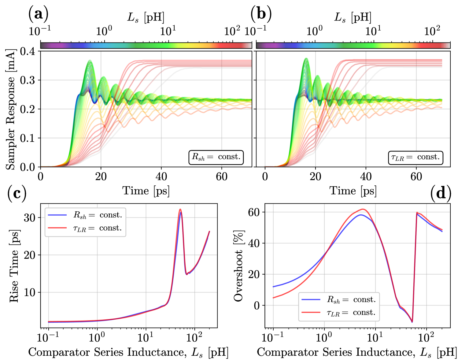
Next we consider inductive coupling via a series inductance (i.e. a pickup coil). As before, values of far below the comparator Josephson inductance pH should not affect operation. Similar to the capacitive coupling case, we may choose to adjust to compensate for shifts in the comparator time constant. In this case the greatest tunable range is yielded by starting with the lowest value that still enforces an underdamped comparator: . Results are shown in Fig. 15 for both a constant shunt of and for an adjusted shunt which maintains the time of the case. The sampler performance is quite similar for both cases and, as in the capacitive-coupling case above, the onset of distortion and degradation occurs once the reactive element (coupling inductor) is no longer a small perturbation compared to the comparator. I.e., the rise time and overshoot are nearly constant until the coupling inductance approaches the comparator’s Josephson inductance pH. Increasing to approximately ten times the comparator results in a moderate reduction in rise time (with little to no impact in overshoot) but for the sampler’s performance is severely impacted.
Appendix E Sampled Waveforms: Strobe Current Bias Sweep
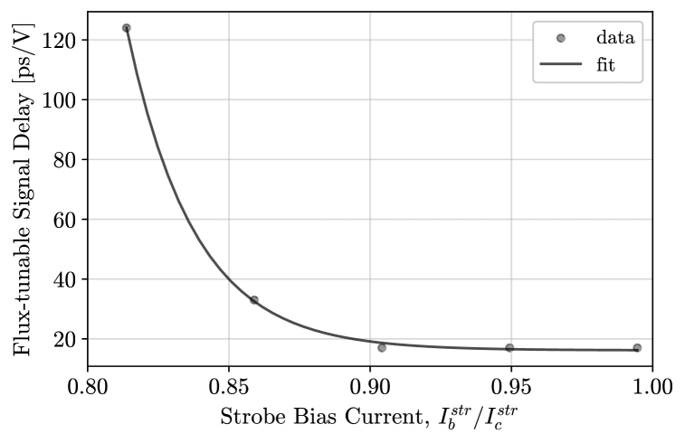
To fully characterize the sampler experimentally, we explore the sampler behavior not only by tuning the DUT current bias as in Sec. IV.3, but also as we vary the strobe current bias, while holding the DUT biases fixed. I.e. the reverse scenario as covered in Sec. IV.3. Strobe and signal alignment in this scenario is more challenging over an instructive range of due to a significant flux-offset-delay calibration nonlinearity. Indeed, the amount of DUT signal advancement (negative delay) per milliamp of dc flux bias applied to the DUT trigger line can be a strong function of the dc strobe current bias. Fig. 16 shows the results of calibrating this effect, performed at each strobe bias point using a tunable mechanical delay line and an exponential fit.
Fig. 17 shows the results of sampling the SQUID DUT, with a fixed SQUID bias, while sweeping the strobe bias. Note the curve in Fig. 17(a) corresponding to (starting y-axis value of 1.5 mA) and its resemblance to measurements in [(15)]. This also corresponds to both the shortest extracted rise time in our device of 3.3 ps and the maximal signal amplitude. However, this waveform displays appreciable distortion relative to the expected dynamics of an underdamped latching SQUID. The analogous measurement of the pulser DUT is shown in Fig. 18. In both cases we observe that for the sampler to accurately reconstruct the target waveform the strobe bias must be and biases below this result in highly distorted sampled waveforms with slow rise (and fall) times.
Appendix F Sampling SFQ Pulses
As an extension to the simulation results detailed in Sec. III.2 we also simulate sampling of an alternate finite time-duration pulse DUT in the form of a DC/SFQ converter. Simulating and experimentally verifying that a Josephson sampler can measure the SFQ output of this type of circuit without significant distortion is most relevant to efforts in superconducting digital logic, computation, and signal generation performed using critically damped JJs. In designing the DC/SFQ converter we chose to maximize the amplitude of the SFQ pulse which results in a pulse with a rise time near the practical maximum for the 0.2 mA/m2JJ process. We maximize the SFQ pulse amplitude by increasing the JJ as this also increases the characteristic voltage and thus the peak voltage of the output SFQ pulse. Pulse-area-quantization means this also shortens the total duration of the SFQ pulse. This is expected to be beneficial in both maximizing the rise time Askerzade (2006) and, in the case such an impulse generator is used to supply the sampling strobe, providing an even larger maximum amplitude pulse than is possible using a Faris pulser. For comparison, our simulated Faris pulser strobe delivers, through the 2 strobe coupling resistor, a peak current pulse of 400 A while the DC/SFQ converter achieves a 600 A pulse.
As in the Faris pulser DUT case, we simulated sampler reconstruction of the target signal as a function of the comparator via tuning . Fig. 19 shows the simulated circuit and simulation results, which echo the findings of Fig. 6. Again, a notable observation is that the sampler is expected to fail to reconstruct the pulser DUT amplitude but should be relatively faithful in measuring the signal FWHM. Finally, we note the similar strong dependence on distortion for sampling finite-duration signals when the comparator is appreciably underdamped ().
Different device variants using all permutations of Faris pulsers and DC/SFQ converters as both the strobe and impulse DUT, designed according to Fig. 19(a), were fabricated on the same wafer as the sampler and DUTs presented in the rest of the text. Measuring the chip variant with a Faris pulser strobe and DC/SFQ DUT, we successfully sample the output of a DC/SFQ converter while operating at 3.6 K. Rather than apply a dc flux offset to the DUT trigger we realize a programmable, tunable strobe-signal delay using a motor-controlled mechanical delay line installed on the strobe trigger. This delay line has a maximum delay of 170 ps and is equipped with a variable follower resistor whose resistance is proportional to the delay.
To minimize hysteresis and position jitter the motor is first driven to its maximum and then minimum delay, after which we begin the sampling measurement. For each strobe-signal trigger delay we step the delay line motor by its minimum increment and only in the forward (increasing strobe delay) direction. The follower resistance is measured to determine the programmed delay at each motor position. The data in Fig. 19(e) were acquired in this manner over three separate scans. Reverse scans were also explored with no observable difference in sampler output. The repeatability of these individual scans is surprisingly consistent but it is clear the minimum motor step is insufficient for sampler measurements targeting a minimum relative delay spacing of ps. We are investigating other methods for sweeping delay to provide 0.1 ps or smaller delay intervals over a wide ( 100 ps) time sweep. The raw sampled pulse data included a small (0 A–7 A), slowly-varying background signal due to on-chip ground bounce and capacitive feedthrough of the trigger signal. This was subtracted from the data presented in Fig. 19(e). To measure this spurious signal the DC/SFQ DUT was sampled both with its dc bias current on (SFQ pulse is output) and with it set to zero (no SFQ pulse is output). For both cases the same input square wave (125 ps period, 50% duty cycle) trigger signal amplitude was provided.
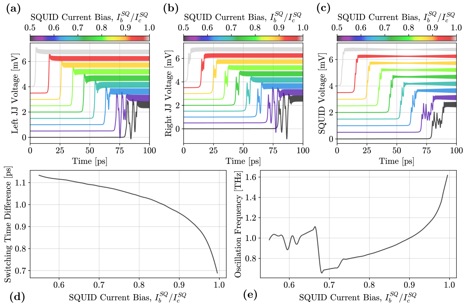
Appendix G SQUID Latching Dynamics
To verify the oscillatory features on the rising edge of the latching SQUID signal observed in Sec. IV.3 we perform simulations, as a function of current bias, of the SQUID DUT alone with its 12 coupling resistor shorted to ground. The SQUID is symmetric with each JJ mA and the flux trigger is a step function pulse with a rise time of 100 ps. Using this simulation we may track each junction’s voltage independently, as well as the total SQUID voltage. These results are shown in Fig. 20, clearly demonstrating that oscillations on the rising edge of the SQUID signal are expected. Furthermore, we also show that these oscillations arise from the delay in switching time – defined here as the time at which the JJ voltage exceeds 10% of the gap voltage of 2.8 mV – between the left and right JJ. Indeed, with the simulated flux coupling inductor polarity and the direction of the screening current, the right JJ switches as much as 1.1 ps before the left JJ switches (Fig. 20(d)) and this delay decreases as is increased. As a final check we again perform a polynomial and sinusoidal fit to the rising edge of the simulated SQUID voltage, this time to the 50%–90% voltage, and obtain the fitted oscillation frequency shown in Fig. 20(e); which also display a distinct transition in frequency. We choose the 50%–90% portion of the SQUID step function in simulation and the portion in measurement to more accurately target the SQUID JJ beat frequency oscillations. In measurement (Fig. 8) these oscillations arise in the central portion of the step and persist at the same frequency up to the very top of the step. For the simulations the beat frequency of interest also appears in the step rising edge, however, once the SQUID has reached it’s asymptotic maximum each JJ is undergoing persistent Josephson oscillations at a frequency above the sampler bandwidth and this masks the beat oscillation. Finally, it is difficult to fit a polynomial to a sharp step function without a large number of terms and this is the reason for choosing only a portion of the signal for performing the fit.
Appendix H Simulations of Sampling Faris Pulser DUT
Our simulation framework is also capable of performing full sampling simulations as a function of DUT bias. This allows us to compare the experimental results of Fig. 8 and Fig. 10 to simulation. As an example we perform a Faris pulser DUT current bias sweep sampler simulation to track the evolution of the sampled waveform. The strobe bias is fixed at . Fig. 21 shows the results of these simulations and we observe high quality agreement with the measurements of Fig. 10. Additionally there is correspondence with the SQUID dynamics simulations detailed in Fig. 20 where at low bias we see multiple complex post-pulse oscillations due to interference in the voltages sources from the two JJs in the Faris pulser’s SQUID. These oscillations become coherent at high bias and are still visible in simulation even at high DUT bias. In experiment we cannot resolve these features once the bias exceeds and we attribute this to the smoothing effects arising from the comparator dynamics convolution with the DUT signal.