Approaching Unity Photon Collection from NV Centers via Ultra-Precise Positioning of Nanodiamonds in Hybrid Nanoantennas
Abstract
Efficient readout of nitrogen-vacancy (NV) centers in diamond is crucial for various quantum information technologies. However, achieving high-fidelity, single-shot readout at room temperature remains challenging due to limited photon collection efficiency (CE) and background noise. In this work, we enhance the readout efficiency of NV centers by integrating them into hybrid metal-dielectric bullseye nanoantennas using ultra-precise deterministic positioning. This approach enables highly directional emission while minimizing optical losses, resulting in a measured CE of 82% into a numerical aperture (NA) as low as 0.5, and approaching unity for NA0.8. This marks a substantial improvement over previous realizations using nanodiamonds, highlighting the advantage of combining hybrid nanoantennas with precise positioning. Our results mark a substantial advancement towards efficient single-shot readout of NV centers by significantly improving readout fidelity and efficiency in a simple on-chip configuration.
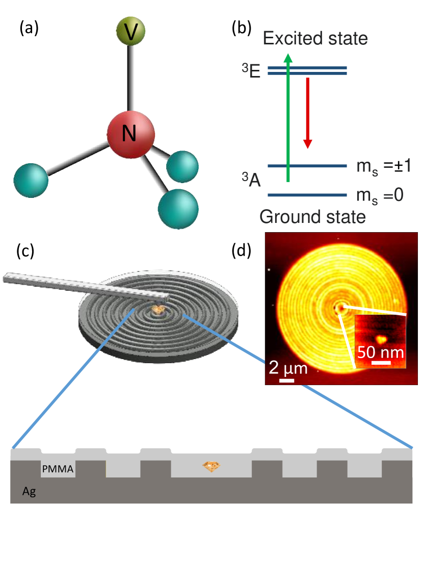
Efficient readout of the spin state of an NV center in diamond is a fundamental challenge in the development of quantum technologies based on NV centers 1. NV centers are point defects in the diamond lattice, characterized by a substitutional nitrogen atom adjacent to a lattice vacancy, as depicted in Figure 1(a). The distinct atomic structure and associated energy levels of an NV center yield a unique combined spin and optical properties, including long spin coherence times as well as spin-dependent fluorescence, as illustrated in Figure 1(b). This combination makes the NV platform a promising candidate for quantum metrology and information processing 2, 3.
However, the emission from the optical transitions of an NV center is inherently non-directional, leading to low photon collection efficiency (CE) and restricting its usability in high-fidelity readout applications. Enhancing CE for low NA optical elements is essential to improve readout fidelity and enable scalable integration of NV centers in quantum devices 4, 5, 6. While previous works have explored various strategies, including dielectric antennas and plasmonic structures, achieving near-unity CE at room temperature remains a challenge due to optical losses and misalignment issues 7, 8, 9, 10.
In this work, we employ a hybrid metal-dielectric nanoantenna combined with ultra-precise deterministic positioning to significantly enhance photon collection from NV centers in nanodiamonds. This approach achieves a measured CE of 82% for NA = 0.5 and CE that approaches unity for NA0.8, demonstrating a substantial improvement in photon extraction efficiency.
Various near-field coupling configurations have been explored to enhance the directionality of quantum emitters. Metal-based nanoantennas 11, 12, 13, 14, 15 provide broadband enhancement due to their small mode volumes and low-quality factors, but suffer from significant ohmic losses 15. Dielectric nanoantennas, while highly directional and low-loss, are inherently limited to narrow-band emitters and often experience strong emission into the high-index dielectric substrate, reducing practical collection efficiency 16, 17, 18, 19.
A hybrid metal-dielectric bullseye nanoantenna offers a unique solution by combining the strengths of both metallic and dielectric structures, achieving high directionality and near-unity CE over a broad spectral range at room temperature 20, 21, 22, 23, 24, 25. The metallic structure enables efficient diffraction over a broad spectral range, enhancing directionality, while the dielectric waveguide layer facilitates photon extraction with minimal nonradiative losses. By integrating NV-containing nanodiamonds into such nanoantennas with ultra-precise positioning, we achieve optimal coupling, resulting in record-high photon extraction efficiencies.
The hybrid metal-dielectric bullseye nanoantenna configuration allows for precise control over the emission pattern, directing the photons into a narrow angular cone, thereby enhancing overall emission efficiency. The rotational symmetry of the bullseye nanoantenna is particularly attractive as it effectively directs the emission of dipole emitters regardless of their XY orientation, ensuring high directivity 22. This dipole orientation insensitive directivity is crucial for NV-based quantum applications requiring high CE, making such a system well-suited for integration with optical fibers and other photonic devices 24. We therefore utilize here ND integrated with such a hybrid metal-dielectric bullseye nanoantenna.
Effective coupling between a quantum emitter and a nanoantenna requires a precise positioning method. Several techniques have been explored for different antenna configurations, such as near-field optical lithography, scanning probe manipulation, and nanowire-based techniques 26, 27, 28, 29, 30, 31, 32, 33. In this study, we utilized a scanning probe-based pick-and-place method, as detailed in the work by Nikolay et al. 34, to deterministically and reproducibly place the NDs onto the nanoantennas with nanometric precision. This technique is both fast and versatile, allowing for high-accuracy placement even on opaque structures. It also enables precharacterization of the emitter, facilitating the selection of suitable emitters for specific applications. Moreover, this method allows for iterative adjustments to the nanoparticle’s position, ensuring deterministic coupling and optimal device performance.
We selected NDs containing NV centers, with a focus on those that house ensembles of NV centers, which are known to enhance sensitivity in sensing applications 35, 36. Additionally, NDs with single NV centers were chosen for their quantum optical characterization. These NDs were then placed on dielectric polymethylmethacrylate (PMMA) coated Ag bullseye antennas developed and detailed in Refs. 37, 23, 21, as shown schematically in Fig 1. An Atomic force microscopy (AFM) scan confirming the successful placement of the ND in the center of the bullseye antenna is shown in Figure 1(d).
After the precise placement of the ND, another PMMA layer is spin-coated on top of the hybrid nanoantenna, forming a complete waveguide layer that contributes to the hybrid metal-dielectric nanostructure. This additional layer enhances the collimation of the emission from the ND, as described in 23. The final configuration, including the ND embedded in the device, is depicted in Figure 1(c), which provides a schematic representation of the ND placement approach and the bullseye antenna structure.
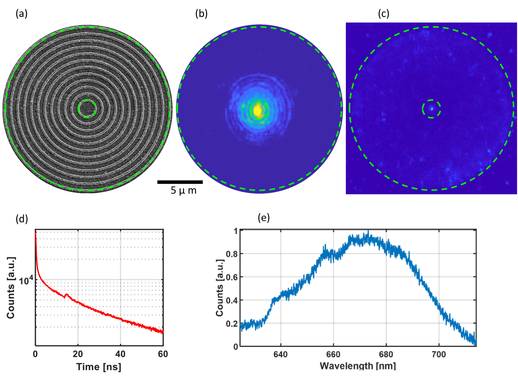
In Figure 2, we present key results from our bullseye nanoantenna coupled with a single ND. Figure 2(a) shows an scanning electron microscope (SEM) image of the fabricated metal part of the bullseye nanoantenna before the deposition of dielectric layers and the positioning of the ND. This image provides a reference for the structural features of the nanoantenna.
Figures 2(b) and 2(c) display a spatial photoluminescence (PL) map and a confocal scan of the antenna with the ND at its center, respectively. These measurements were performed with a single nanodiamond (ND), which contains one or more NV centers. Figure 2(b) was obtained using a tightly focused 532 nm continuous-wave (CW) diode laser for excitation, while Figure 2(c) was obtained using a pulsed laser with a repetition rate of 5 MHz, omitting counts during the first 2 nanoseconds after each laser pulse to reduce background noise. The NV center emission was filtered using a combination of a 620 nm short-pass and a 720 nm long-pass filter and collected using an objective lens with a NA of 0.9. The consistent scaling and centering across these images, along with the SEM image in Figure 2(a), allow for a direct visual correlation between the physical layout of the nanoantenna and the observed PL results, effectively illustrating the coupling effects achieved.
The dashed green lines in Figure 2(a) mark the first and last circular gratings of the bullseye structure, providing a visual guide to the extent of the nanoantenna. This marking is crucial for understanding the spatial confinement and the role of the nanoantenna in directing the emission, as also demonstrated in similar studies such as those by Abudayyeh et al. on deterministic placement of quantum dots in nanoantennas 23 and by Nikolay et al. on the accurate placement of single nanoparticles on opaque conductive structures 34. The images confirm the findings that fluorescence is primarily emitted from the central region of the bullseye structure, highlighting the precise positioning of the ND and the efficient coupling achieved in the device.
Figures 2(d) and 2(e) present measurements of fluorescence lifetime and emission spectrum, respectively. These measurements, performed using a 532 nm pulsed laser, reveal the characteristic NV emission spectrum at room temperature. The emission spectrum, shown in Figure 2(e), later provides the weightings for different emission wavelengths in the simulation of the back focal plane image, shown in Figure 4(d). This precise mapping of emission is essential for optimizing device performance, particularly in quantum applications that rely on controlled photon emission and high CE.
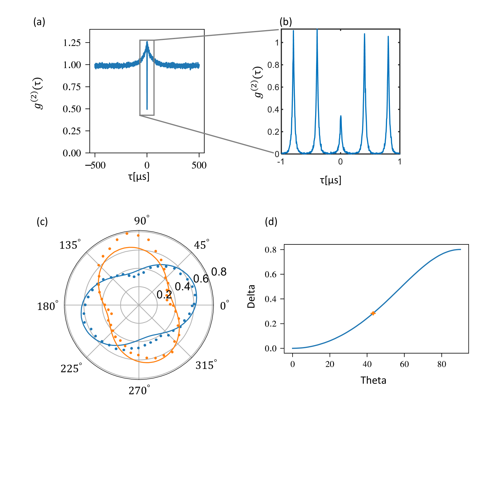
Figure 3(a) shows second order correlation measurement for a time scale longer than the lifetime of the NV center emission, using pulsed laser at a repetition rate of 2.5 MHz. Figure 3(b) displays a zoom into short delay times, showing a clear antibunching behavior which confirms that indeed there is only single NV center emitting in this device. The shelving in a metastable singlet state (not shown in Fig. 1(b)) leads to the observation of photon bunching with longer timescales 38. Following 39, we used a half-wave plate and a polarizing beam-splitter to separate the PL into two arms. Each arm leads to a single-photon counting avalanche photodiode. By rotating the half-wave plate we measured simultaneously the x- and y-polarized emission of the same emitter for different angles. Figure 3(c) shows a polar plot of intensity as a function of the polarization analysis angle for two perpendicular polarizations. We simulated two crossed dipoles of NV center, covered in PMMA. Based on this simulation, Figure 3(d) presents a map of degree of polarization () and expected angle () of the NV center crossed linear dipoles.
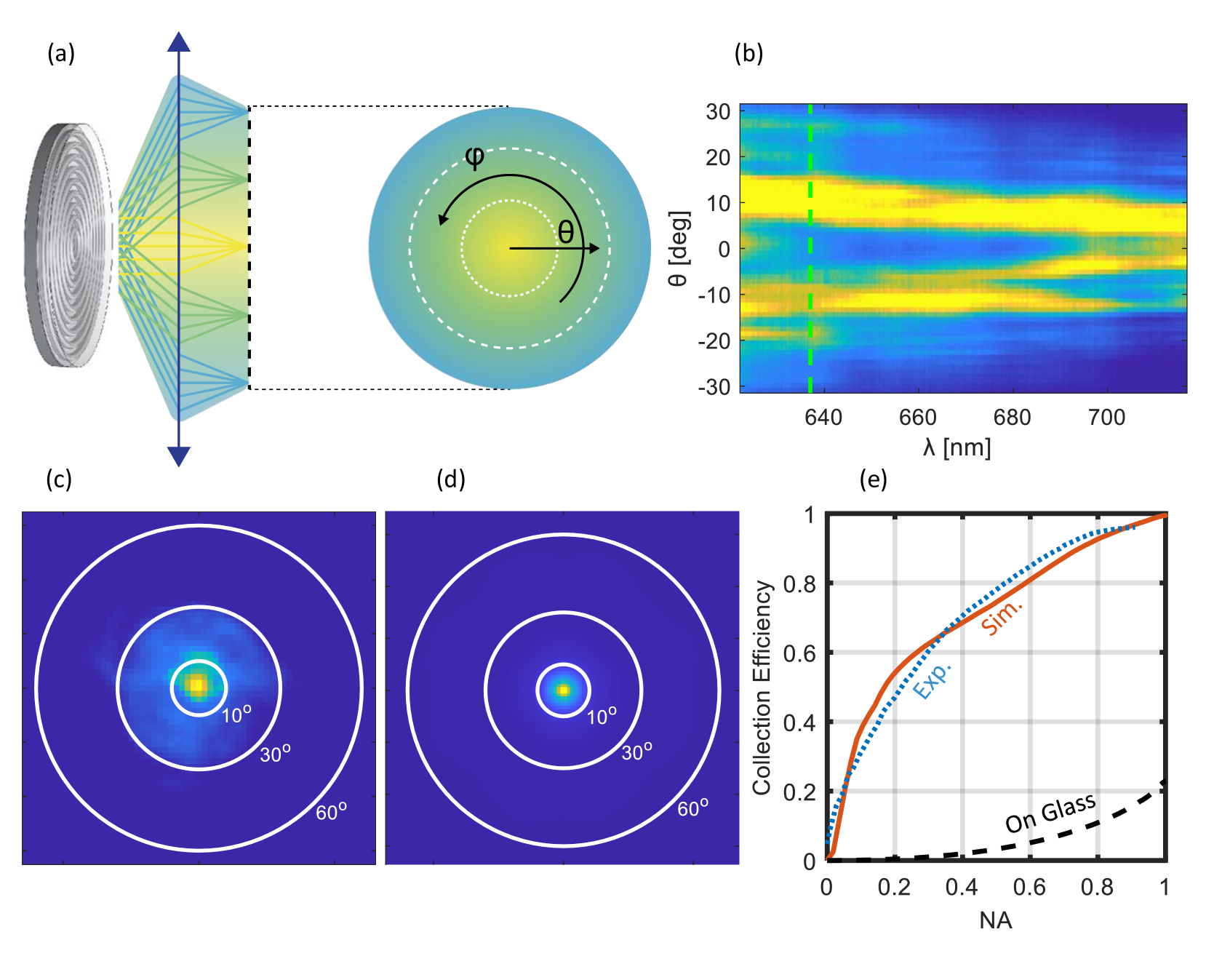
Figure 4 examines the PL directionality and collection efficiency of the device, analyzing how emitted photons are distributed and efficiently collected. To investigate this, we measured the PL directionality emitted from the device using back focal plane imaging, which provides a 2D angular PL intensity distribution , where and are the polar and azimuthal angles, respectively (Figure 4(a)) 23, 24. Figure 4(b) shows a spectrally resolved 1D cross section of the back focal plane of the device PL, capturing the broad spectral range of 620-720 nm, which includes the zero-phonon line of NV centers at 637 nm (marked with a dashed green line). The data indicates a broadband narrow angular emission pattern around 700 nm. Additionally, the PL emission over the entire measured spectrum is largely confined within 10 degrees from the normal, highlighting the broadband operational capability of the nanoantenna. Figures 4(c) and 4(d) display the spectrally integrated back focal plane images of the angular PL intensity distribution for the measured wavelength range of 620-720 nm, illustrating the highly directional nature of the emitted photons.
The simulation visualized in Figure 4(d), using an FDTD numerical solution of a broadband optical dipole positioned in such a nanoantenna, with the experimental parameters of the actual device. We incorporated the NV spectrum measured in Figure 2(e), using the measured spectral intensities as weights for the simulation data of each wavelength, and then incoherently sum the simulated intensities of all wavelengths. Additionally, the dipole orientation was fixed at , based on the experimental estimation from the angular emission pattern, as detailed in Figures 3(c) and 3(d).
The CE of the emitted light was analyzed as a function of the NA of the collection optics. This was done by integrating the experimental and simulated signal over all azimuthal angles within a collection cone defined by a given NA, using:
| (1) |
This equation, as detailed in previous studies, provides a measure of the proportion of emitted photons that can be collected into a given NA 24, 23.
Figure 4(e) presents the CE as a function of NA for our device. The results demonstrate a CE of approximately 80% at NA=0.5, indicating a very high directionality of the emitted photons. This performance is compared to FDTD simulation results, which show good agreement with the experimental data. In contrast, a simulation of a reference NV center placed on a glass slide (indicated by the black dashed line) shows significantly lower CE, underscoring the superior performance of our nanoantenna design. We note that the very high accuracy 34 positioning method we use, allows near-optimal utilization of the nanoantenna capabilities, resulting in high CE for a broad spectrum emission into low NA optics. This allows the use of very simple collection optics and even direct coupling into an optical fiber 24.
In summary, we demonstrated a hybrid metal-dielectric nanoantenna platform combined with ultra-precise deterministic positioning to significantly enhance photon collection from NV centers in nanodiamonds. Our approach achieves a measured CE of 82% for NA = 0.5 and CE that approaches unity for NA0.8 at room temperature.
This work highlights the importance of optimizing both the position of the emitter by precise nano-placement and the antenna performance by a hybrid design, enabling highly directional emission while minimizing optical losses. The combination of broadband operation, high efficiency, polarization independence, and room-temperature compatibility is essential when utilizing NV centers in integrated quantum devices, such as for single-shot spin readout or high-rate entanglement distribution in quantum networks.
Acknowledgments
NN and OB acknowledge funding by BMBF 16KISQ003 (QR.X).
References
- Wolf et al. 2015 Wolf, S. A.; Rosenberg, I.; Rapaport, R.; Bar-Gill, N. Purcell-enhanced optical spin readout of nitrogen-vacancy centers in diamond. Physical Review B - Condensed Matter and Materials Physics 2015, 92, 1–5
- Doherty et al. 2013 Doherty, M. W.; Manson, N. B.; Delaney, P.; Jelezko, F.; Wrachtrup, J.; Hollenberg, L. C. L. The nitrogen-vacancy colour centre in diamond. Physics Reports 2013, 528, 1–45
- Guo 2023 Guo, S. An Overview of NV Centers. Journal of Applied Mathematics and Physics 2023, 11, 3666–3675
- Hausmann et al. 2012 Hausmann, B. J. M.; Shields, B.; Quan, Q.; Maletinsky, P.; McCutcheon, M.; Choy, J. T.; Babinec, T. M.; Kubanek, A.; Yacoby, A.; Lukin, M. D.; Lončar, M. Integrated Diamond Networks for Quantum Nanophotonics. Nano Letters 2012, 12, 1578–1582
- Li et al. 2023 Li, Y.; Gerritsma, F. A.; Kurdi, S.; Codreanu, N.; Gröblacher, S.; Hanson, R.; Norte, R.; van der Sar, T. A Fiber-Coupled Scanning Magnetometer with Nitrogen-Vacancy Spins in a Diamond Nanobeam. ACS Photonics 2023, 10, 1859–1865
- Dhomkar et al. 2024 Dhomkar, S.; Ji, W.; Kim, D.; Barry, J. F.; Walsworth, R. L. Efficient readout of nitrogen-vacancy spin qubits in diamond. Science Advances 2024, 10, eadp6442
- Robledo et al. 2011 Robledo, L.; Childress, L.; Bernien, H.; Hanson, R.; Hensen, B.; Taminiau, T. H. High-fidelity projective read-out of a solid-state spin quantum register. Nature 2011, 477, 574–578
- Hensen et al. 2015 Hensen, B. et al. Loophole-free Bell inequality violation using electron spins separated by 1.3 kilometres. Nature 2015, 526, 682–686
- Hopper et al. 2018 Hopper, D. A.; Shulevitz, H. J.; Bassett, L. C. Spin Readout Techniques of the Nitrogen-Vacancy Center in Diamond. Micromachines 2018, 9, 437
- Zhang et al. 2021 Zhang, Q.; Guo, Y.; Ji, W.; Wang, M.; Yin, J.; Kong, F.; Lin, Y.; Yin, C.; Shi, F.; Wang, Y.; Du, J. High-fidelity single-shot readout of single electron spin in diamond with spin-to-charge conversion. Nature Communications 2021, 12, 1529
- Nepal et al. 2013 Nepal, D.; Drummy, L. F.; Biswas, S.; Park, K.; Vaia, R. A. Large scale solution assembly of quantum dot-gold nanorod architectures with plasmon enhanced fluorescence. ACS Nano 2013, 7, 9064–9074
- Hoang et al. 2015 Hoang, T. B.; Akselrod, G. M.; Argyropoulos, C.; Huang, J.; Smith, D. R.; Mikkelsen, M. H. Ultrafast spontaneous emission source using plasmonic nanoantennas. Nature Communications 2015, 6
- Ahmed et al. 2012 Ahmed, S. R.; Cha, H. R.; Park, J. Y.; Park, E. Y.; Lee, D.; Lee, J. Photoluminescence enhancement of quantum dots on Ag nanoneedles. Nanoscale Research Letters 2012, 7, 1–7
- Guo et al. 2015 Guo, R.; Derom, S.; Väkeväinen, A. I.; van Dijk-Moes, R. J. A.; Liljeroth, P.; Vanmaekelbergh, D.; Törmä, P. Controlling quantum dot emission by plasmonic nanoarrays. Optics Express 2015, 23, 28206
- Bitton et al. 2019 Bitton, O.; Gupta, S. N.; Haran, G. Quantum dot plasmonics: From weak to strong coupling. Nanophotonics 2019, 8, 559–575
- Skolnick et al. 1998 Skolnick, M. S.; Fisher, T. A.; Whittaker, D. M. Strong coupling phenomena in quantum microcavity structures. Semiconductor Science and Technology 1998, 13, 645–669
- Press et al. 2007 Press, D.; Götzinger, S.; Reitzenstein, S.; Hofmann, C.; Löffler, A.; Kamp, M.; Forchel, A.; Yamamoto, Y. Photon antibunching from a single quantum-dot-microcavity system in the strong coupling regime. Physical Review Letters 2007, 98, 1–4
- Bogdanović et al. 2017 Bogdanović, S.; Van Dam, S. B.; Bonato, C.; Coenen, L. C.; Zwerver, A. M. J.; Hensen, B.; Liddy, M. S. Z.; Fink, T.; Reiserer, A.; Lončar, M.; Hanson, R. Design and low-temperature characterization of a tunable microcavity for diamond-based quantum networks. Applied Physics Letters 2017, 110
- Jun et al. 2011 Jun, Y. C.; Huang, K. C. Y.; Brongersma, M. L. Plasmonic beaming and active control over fluorescent emission. Nature Communications 2011, 2
- Livneh et al. 2015 Livneh, N.; Harats, M. G.; Yochelis, S.; Paltiel, Y.; Rapaport, R. Efficient Collection of Light from Colloidal Quantum Dots with a Hybrid Metal-Dielectric Nanoantenna. ACS Photonics 2015, 2, 1669–1674
- Livneh et al. 2016 Livneh, N.; Harats, M. G.; Istrati, D.; Eisenberg, H. S.; Rapaport, R. Highly Directional Room-Temperature Single Photon Device. Nano Letters 2016, 16, 2527–2532
- Abudayyeh and Rapaport 2017 Abudayyeh, H.; Rapaport, R. Quantum Emitters Coupled to Circular Nanoantennas for High Brightness Quantum Light Sources. Quantum Science and Technology 2017, 2, 034004
- Abudayyeh et al. 2021 Abudayyeh, H.; Lubotzky, B.; Blake, A.; Wang, J.; Majumder, S.; Hu, Z.; Kim, Y.; Htoon, H.; Bose, R.; Malko, A. V.; Hollingsworth, J. A.; Rapaport, R. Single photon sources with near unity collection efficiencies by deterministic placement of quantum dots in nanoantennas. APL Photonics 2021, 6, 036109
- Lubotzky et al. 2024 Lubotzky, B.; Nazarov, A.; Abudayyeh, H.; Antoniuk, L.; Lettner, N.; Agafonov, V.; Bennett, A. V.; Majumder, S.; Chandrasekaran, V.; Bowes, E. G.; Htoon, H.; Hollingsworth, J. A.; Kubanek, A.; Rapaport, R. Room-Temperature Fiber-Coupled Single-Photon Sources based on Colloidal Quantum Dots and SiV Centers in Back-Excited Nanoantennas. Nano Letters 2024, 24, 640–648
- Waltrich et al. 2021 Waltrich, R.; Lubotzky, B.; Abudayyeh, H.; Steiger, E. S.; Fehler, K. G.; Lettner, N.; Davydov, V. A.; Agafonov, V. N.; Rapaport, R.; Kubanek, A. High-purity single photons obtained with moderate-NA optics from SiV center in nanodiamonds on a bullseye antenna. New Journal of Physics 2021, 23, 113022
- Sipahigil et al. 2016 Sipahigil, A. et al. An integrated diamond nanophotonics platform for quantum-optical networks. Science 2016, 354, 847–850
- Gschrey et al. 2013 Gschrey, M.; Gericke, F.; Schüßler, A.; Schmidt, R.; Schulze, J. H.; Heindel, T.; Rodt, S.; Strittmatter, A.; Reitzenstein, S. In situ electron-beam lithography of deterministic single-quantum-dot mesa-structures using low-temperature cathodoluminescence spectroscopy. Applied Physics Letters 2013, 102
- Shi et al. 2016 Shi, Q.; Sontheimer, B.; Nikolay, N.; Schell, A. W.; Fischer, J.; Naber, A.; Benson, O.; Wegener, M. Wiring up pre-characterized single-photon emitters by laser lithography. Scientific Reports 2016, 6, 1–7
- Harats et al. 2017 Harats, M. G.; Livneh, N.; Rapaport, R. Design, fabrication and characterization of a hybrid metal-dielectric nanoantenna with a single nanocrystal for directional single photon emission. Optical Materials Express 2017, 7, 834
- Schell et al. 2011 Schell, A. W.; Kewes, G.; Schröder, T.; Wolters, J.; Aichele, T.; Benson, O. A scanning probe-based pick-and-place procedure for assembly of integrated quantum optical hybrid devices. Review of Scientific Instruments 2011, 82
- Cuche et al. 2009 Cuche, A.; Sonnefraud, Y.; Faklaris, O.; Garrot, D.; Boudou, J. P.; Sauvage, T.; Roch, J. F.; Treussart, F.; Huant, S. Diamond nanoparticles as photoluminescent nanoprobes for biology and near-field optics. Journal of Luminescence 2009, 129, 1475–1477
- Van Der Sar et al. 2009 Van Der Sar, T.; Heeres, E. C.; Dmochowski, G. M.; De Lange, G.; Robledo, L.; Oosterkamp, T. H.; Hanson, R. Nanopositioning of a diamond nanocrystal containing a single nitrogen-vacancy defect center. Applied Physics Letters 2009, 94, 10–13
- Huck et al. 2011 Huck, A.; Kumar, S.; Shakoor, A.; Andersen, U. L. Controlled coupling of a single nitrogen-vacancy center to a silver nanowire. Physical Review Letters 2011, 106, 2–5
- Nikolay et al. 2018 Nikolay, N.; Sadzak, N.; Dohms, A.; Lubotzky, B.; Abudayyeh, H.; Rapaport, R.; Benson, O. Accurate placement of single nanoparticles on opaque conductive structures. Applied Physics Letters 2018, 113, 113107
- Webb et al. 2020 Webb, J. L.; Troise, L.; Hansen, N. W.; Achard, J.; Brinza, O.; Staacke, R.; Kieschnick, M.; Meijer, J.; Perrier, J. F.; Berg-Sørensen, K.; Huck, A.; Andersen, U. L. Optimization of a Diamond Nitrogen Vacancy Centre Magnetometer for Sensing of Biological Signals. Frontiers in Physics 2020, 8, 1–12
- Taylor et al. 2008 Taylor, J. M.; Cappellaro, P.; Childress, L.; Jiang, L.; Budker, D.; Hemmer, P. R.; Yacoby, A.; Walsworth, R.; Lukin, M. D. High-sensitivity diamond magnetometer with nanoscale resolution. Nature Physics 2008, 4, 810–816
- Harats et al. 2017 Harats, M. G.; Livneh, N.; Rapaport, R. Design, fabrication and characterization of a hybrid metal-dielectric nanoantenna with a single nanocrystal for directional single photon emission. Optical Materials Express 2017, 7, 834–843
- Thiering and Gali 2018 Thiering, G.; Gali, A. Theory of the optical spin-polarization loop of the nitrogen-vacancy center in diamond. Physical Review B 2018, 98, 1–12
- Lethiec et al. 2014 Lethiec, C.; Laverdant, J.; Vallon, H.; Javaux, C.; Dubertret, B.; Frigerio, J. M.; Schwob, C.; Coolen, L.; Maître, A. Measurement of three-dimensional dipole orientation of a single fluorescent nanoemitter by emission polarization analysis. Physical Review X 2014, 4, 1–12