On the role of Electronic Doorway States
in the Secondary Electron Emission from Solids
Abstract
We investigate the phenomenon of secondary low-energy electron emission from graphene and graphite. By applying a coincidence detection of the primary scattered and an emitted secondary electron, we disentangle specific features otherwise hidden in the essentially featureless secondary electron spectrum. Hand-in-hand with density functional theory calculations, we show that this slow electron emission is governed not only by the density of states in the occupied and unoccupied band structure but is also modulated by the coupling of levels above the vacuum energy to free-vacuum states. This implies electronic doorway states which facilitate efficient propagation of electrons from the solid to vacuum, some of which only open for samples with more than 5 layers.
Low-energy (secondary) electrons (LEEs) are integral to today’s research and industry, especially in microscopy and nanotechnology. For example, the imaging contrast in scanning electron microscopy (SEM, Everhart-Thornley detectors) [1, 2, 3] and helium ion microscopy (HIM) [4, 5, 6] relies on emitted secondary LEEs. Other relevant techniques include electron-beam-induced chemical processes [7, 8] and deposition techniques (e.g. focused-electron-beam-induced deposition (FEBID)) [9, 10]) or LEE-driven damage in biomolecules [11, 12], among many others. Despite the immense importance of LEEs in various biological, chemical and physical processes there exists a lack of understanding of the underlying mechanisms which lead to the energy profile of LEEs emitted from solid surfaces.
There is a plethora of literature concerning LEE emission from surfaces in general [13, 14, 15], many focusing on carbon-based materials like graphite [16, 17, 18, 18]. Graphite is also used in many applications due to its low secondary electron yield, e.g. for electron optics and wall material in charged particle storage rings, where multipacting is a well-known issue and needs to be reduced to a minimum [19, 20]. While many LEE spectra consist of a mainly featureless energy distribution, graphite stands out due to a very distinct and non-dispersive feature at eV [21, 22]. This X-peak is a result of plasmon excitation and subsequent decay, which leads to the hybridisation of above-vacuum atom-like states (with a high density of states but no mobility) and interlayer states [22]. Accordingly, this feature should change for small numbers of material layers and, ultimately, vanish for a single layer of graphene, where interlayer states naturally do not exist. Here we show experimentally and theoretically that this is indeed true, but go one significant step further and demonstrate that the emission spectrum of LEEs is not only a result of the above-vacuum density of states of the solid, but is significantly modulated by a state-dependent coupling to plane wave vacuum states. We quantify the corresponding coupling strength for single-layer and bilayer graphene, and graphite at the point for all states between the vacuum energy and eV. From the underlying fact that for any solid-to-vacuum transition the Fourier components of the electron wave function in the solid and the vacuum should show some matching, it follows that the LEE spectral modulation is a general phenomenon for all material surfaces.
In this work, we explore the LEE emission from graphite by means of correlated electron spectroscopy not only using the bulk material but also single- and bilayers thereof. By applying density functional theory (DFT) calculations, we discuss that the band dispersion and density of states (DOS) alone do not suffice to describe the appearing energy features. Instead, material-specific (and layer-number-specific) doorway states allow the leaking of the above-vacuum states to vacuum.
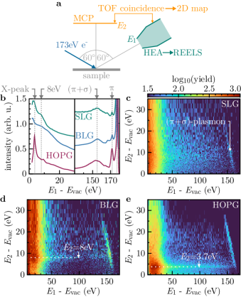
For the experiments, we used quasi-freestanding single layer graphene (SLG) and bilayer graphene (BLG). The samples were fabricated by annealing epitaxial grown zero-layer and monolayer graphene on 4H-SiC(0001) in hydrogen atmosphere at 550 °C and 860 °C, respectively. The graphene used as a precursor was produced by adapting the procedure from Kruskopfet al. [23]. Additionally, we performed measurements using a highly-oriented pyrolitic graphite (HOPG) sample, which has ZYB quality with a nominal mosaic spread of and was mechanically exfoliated in air before being introduced in the vacuum chamber. All samples were annealed under ultra-high vacuum conditions at C (HOPG) and C (SLG, BLG) prior to and several times during week-long measurements. FIG. 1 (a) shows the experimental geometry used to assess (correlated) electron emission: 173 eV electrons are scattered from a surface, and their energy () is measured using a hemispherical energy analyser (HEA) at with respect to the sample surface normal, which corresponds to a Bragg maximum for this geometry. A microchannel plate (MCP) detector with a RoentDek delay line anode is placed normal to the surface and provides the energy information of a second electron () for coincidence measurements using a time-of-flight (TOF) approach (cf. Supplementary Material of [22]). In general, due to the indistinguishability of electrons, the emitted particles cannot be identified as ‘reflected electron’ or ‘secondary electron’. For simplification, however, LEEs (left half of FIG. 1 (b)) are often termed ‘secondary electrons’, while electrons closer to the primary energy are regarded as ‘reflected’ electrons or the ‘energy loss part’ of the spectrum. Note that this differentiation affects the energy scales of the respective data, as only in the case of secondary electrons does the work function of the material need to be accounted for. Low currents of 2.6 pA were used for coincidence studies to ensure a reasonable true-to-false ratio on the order of unity.
FIG. 1 (b) shows reflection electron energy loss spectroscopy (REELS) results for all three materials for a primary beam of 173 eV electrons. The secondary electron spectra (left half) look different for the three materials; however, except for the 3.7 eV peak with HOPG (red, the so-called ‘X-peak’ [24]), no distinct features are clearly visible. The right half shows the energy loss part of the spectrum. The elastic peak is cut off to better display the - and )-plasmon peaks. Small peaks/shoulders indicate double and triple plasmon excitation.
Corresponding maps for SLG, BLG and HOPG measured under identical conditions are displayed in FIG. 1 (c)-(e). In all three maps, we can identify an island around eV and eV, representing the excitation and direct decay of a -plasmon. The -plasmon excitation, additionally visible in panel (b), is not present in the coincidence maps because, for the given experimental geometry, direct decay of the -plasmon is not kinematically possible, as previously discussed in [22].
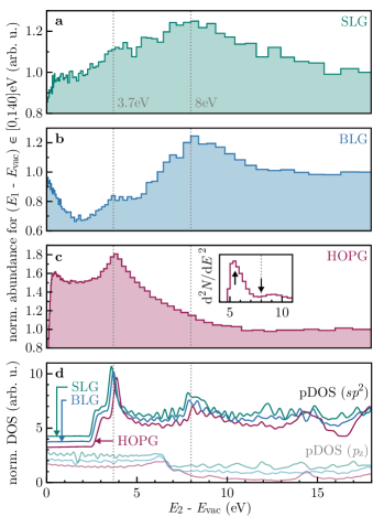
For the secondary electrons, where in the REELS spectrum only HOPG exhibits the strong X-peak, the maps present a distinct feature also for BLG at a different energy of 8 eV. This feature is also clearly apparent in the projected spectra shown in FIG. 2, where we integrated over the range eV for all three materials. For SLG (a), the energy distribution is washed out without any significant features, while for BLG (b), there is an asymmetric peak at 8 eV and a small hinted peak at 3.7 eV, which corresponds to the energy of the ‘X-peak’ in HOPG (c). Different smaller windows do not lead to significant changes in the spectra, as can be seen in Appendix A. The absence of dispersion in demonstrates that the low-energy electron emission in graphite samples does not underlie direct scattering kinematics of the two electrons but is rather driven by plasmon excitation and subsequent decay.
At this point, let us briefly revisit the steps leading to the emission of the secondary electrons into vacuum: Under the given geometry, coincidences are mainly recorded for electrons which first get elastically scattered on one of the first material layers before inelastically scattering, predominantly through plasmon excitation on the ‘way out’. This procedure is described in the deflection and loss (D+L) model [25, 26, 27, 28]. The plasmon can either directly decay via emission of an electron (cf. the island in the maps in FIG. 1) or elevate an electron into an excited (above-vacuum) state. These excited electrons can couple to free vacuum states to leave the material. To understand the final energy distribution we thus have to consider two steps: (1) the population of excited above-vacuum material band structure states and (2) the coupling strength of the respective states to vacuum. Only if both criteria are favoured, there is a successful emission of electrons with the given kinetic energy.
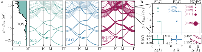
To elucidate the origin of the different emission patterns for the different materials, we calculate the electronic structure of SLG, BLG and HOPG. The band structure, DOS (both in FIG. 3), and projected density of states (pDOS) 2 (b) were calculated using the Vienna ab-initio software package (VASP) (see Appendix. B for details).
After electronic excitation, or even plasmonic excitation with subsequent liberation of a solid-state electron, the final secondary electron occupies an excited state within the material (HOPG, BLG or SLG). Clearly, the density of electronic states provides a first-order estimate of the distribution of electronic energies. Indeed, all three materials feature a substantial DOS peak at eV above vacuum, as well as a second peak at eV above vacuum. Given their similarity, the density of states alone cannot explain experimental observations (cf. FIG. 2). However, to be detected as secondary electron requires escape from the surface with a final velocity suited to reach the detector.
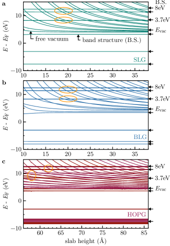
To calculate the coupling of excited states to vacuum, we next consider a slab calculation, with slab height consisting of the material itself and a length of vacuum separating the periodic simulated slabs by vacuum in -direction normal to the layers surfaces. The electronic structure is a combination of electronic states inside the material, and standing waves within the vacuum region, see FIG. 3. While the energy of the former does not depend on , the energy of the standing waves strongly varies with with , see App. B. Consequently, evaluating the Kohn-Sham eigenenergies as a function of , allows for disentangling both contributions. Furthermore, (avoided) crossings emerge between the plane wave vacuum states and conduction-band states within the material. The magnitude of these avoided crossings provides an estimate for the coupling strength between the vacuum and the conduction-band state.
For SLG and BLG, we find no significant crossings between the conduction band states at around 3.7 eV above vacuum, see FIG. 3 (b), in line with the lack of a peak in secondary electron emission at this energy. However, for HOPG, there is a substantial avoided crossing, again in line with the prominent emission of secondary electrons at this energy in the experiment.
The origin of this prominent crossing are the dispersive states of HOPG in -direction, with maximum amplitudes in-between the layers within HOPG. These states strongly interact with the plane-wave states of the vacuum, in line with earlier investigations [22]. They thus form a doorway for electrons excited into the DOS peaks at 3.7 eV above vacuum, to further proceed towards free vacuum states outside the material. Consequently, we conjecture that for BLG and SLG, the scattering-cross section to excite electrons into conduction-band states at these energy is not zero. Instead, there is a lack of secondary electron emission at this energy because excited electrons cannot get out, as there is no doorway for few-layer systems. Our slab calculations show that the corresponding dispersive interlayer states in direction, i.e. perpendicular to the layers, emerges for HOPG slabs only after including five layers or more.
Also the peak at 8 eV above vacuum is consistent with these findings: Here, also BLG features an albeit small but nevertheless clearly non-zero avoided crossing between BLG and vacuum states, consistent with the appearance of a peak in secondary electron emission at this energy. Since this crossing is smaller for HOPG by an order of magnitude than the one at 3.7 eV, there is no apparent 8 eV-peak for HOPG. The number of emitted electrons at the 3.7 eV feature is just so much bigger - although careful analysis, indeed, shows a feature also at 8 eV in the double-differential spectrum (see FIG. 1 and inset for HOPG in Fig. 2).
FIG. 2 (d) shows the pDOS on and orbitals. Indeed, especially for the orbitals, there are features at both relevant energies 3.7 eV and 8 eV, the first one being more pronounced. In contrast, for the orbitals the pDOS only exhibits one step at eV, where there is no feature present in any experimental spectrum. There are no apparent differences either in the pDOS or in the total DOS (shown for SLG as representative in the left panel of FIG. 3 (a)) for the three materials, which indicates that the population of excited states should proceed similarly. The same applies for the full band structure of the material slabs (full lines) shown in FIG. 3 (a) together with free vacuum states (transparent lines).
Hence, we will now regard the second criterion for secondary electron emission: Coupling to free vacuum states. As a measure, we analyse the matrix element of band structure and vacuum states for different simulation slab heights (cf. Appendix B), shown in FIG. 3 (b). For SLG, there is no measurable interaction, i.e., the matrix elements for all relevant crossings are meV, which we define as ’no crossing’ (crosses in the graph). For BLG, there is no crossing for the energy level at 3.7 eV but we find an avoided crossing at eV. For HOPG, there is an avoided crossing for all energies, with the 3.7 eV-feature exhibiting the strongest coupling (by an order of magnitude).
Both criteria combined, we can now explain the electron emission behaviour observed in experiment: For all three samples, plasmon decay populates the unoccupied band structure above vacuum, which does not differ significantly for the three samples of different layer numbers. For SLG, there is no particular doorway state favouring the propagation to free vacuum states, which leads to the washed out energy spectrum (FIG. 2). In the case of BLG, electrons excited in the bands around 8 eV can escape to vacuum efficiently. Note that the asymmetry seen for the 8 eV-peak for BLG in FIG. 2 is resembled by the corresponding peak in the pDOS in the lowest panel of the same figure; indicating that indeed all unoccupied states are populated.
For the pDOS, the most prominent peak for all samples is around eV. However, only for HOPG there is a dominant coupling of this state to vacuum. A closer look at FIG. 3 (b) reveals that in addition to the 3.7 eV-feature, there is also substantial coupling for states at eV and eV. At these energies, there are no obvious shoulders in the 2 spectrum in FIG. 2, but the second derivative (cf. insert) shows peculiarities in both cases.
The present work highlights the power of coincidence spectroscopy, which lets us resolve structures in the LEE spectrum otherwise hidden in a broad background of the inelastic secondary electron cascade. In this way, we cannot only identify that the dominating emission properties are plasmon-mediated but also that there are noteworthy differences in the LEE spectrum shape for materials. While it is known that the above-vacuum band structure plays a role in the emission process [21, 29, 22], we add here a second criterion necessary to be considered: Coupling to vacuum states. Our results show, that there are doorway states which open only above a certain threshold number of layers - the most dominant doorway leading to the ‘X-peak’ in HOPG has a threshold at around 5 layers. The applied DFT approach to calculate this coupling is universal and can be adapted to other materials to predict energy spectra of secondary electrons.
Our findings mark an important step to disentangle the LEE emission spectrum which is rich in information about the surface and it’s electronic structure. We provide an understanding of how a LEE spectrum is formed and pave a way to tailor the LEE spectrum for example by reducing the layer number in van der Waals type materials.
Acknowledgements.
The authors acknowledge funding from the Austrian Science Fund (FWF) through the doctoral college 10.55776/DOC142 and the Grant DOI 10.55776/Y1174. The computational results presented have been achieved using the Vienna Scientific Cluster (VSC).Appendix A Energy Dispersion of -Peaks
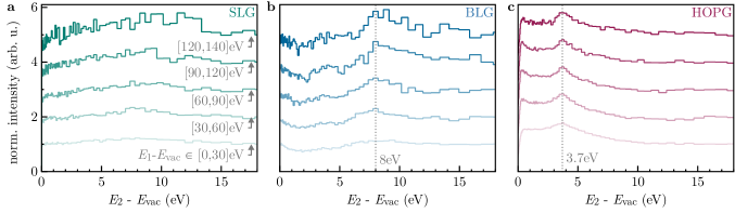
To investigate the dispersion of the horizontal features in the maps in FIG. 1, we integrated all counts in different ranges. eV is considered as maximum energy to prevent an overlap with the -plasmon islands. FIG. 4 shows these projected spectra for the single-, bilayer and HOPG sample. For SLG, the spectrum is featureless for all five ranges. The 8 eV and 3.7 eV peak for BLG and HOPG, respectively, is visible in all spectra without significant energy dispersion and changes of the peak shapes.
Appendix B Coupling of band structure to free vacuum states
We consider slab calculations of HOPG, BLG and SLG, with periodic boundary conditions in all three spatial directions. We choose the -axis perpendicular to the surface. The height of the slab is thus the sum of the height of the material itself, comprised of 1 (SLG), 2 (BLG), or 12 (for HOPG) graphene layers, and the vacuum separating the block of material from its periodic replicas in direction. Since we require an accurate model of wave functions above the Fermi level, we employ a large plane-wave energy cutoff of 1200 eV, and a -point Monkhorst grid of for HOPG and for SLG and BLG. The supercell for HOPG consists of two layers of carbon atoms in Bernal stacking, forming a hexagonal lattice with a lattice constant of 2.47 Å and an interlayer spacing of 3.4 Å. Above the Fermi level, the associated electronic structure features virtual conduction band states as well as delocalised vacuum states for energies above the work function of the solid. We consider Åto avoid finite-size effects in -direction. The energy of conduction band (CB) states then only weakly depends on . However, a finite results in quantization of the vacuum states (vac) as standing waves in -direction, with , where . Consequently, calculating Kohn Sham eigenenergies as a function of provides a way to disentangle both states, see Fig. 5: while the conduction-band states appear as (almost) horizontal lines, the scale approximately as
| (1) |
Consequently, (avoided) crossings of the vacuum levels with conduction-band states have to emerge, as known from atomic physics: the size of these avoided crossings determines the coupling, and thus the interaction strength between the vacuum state and the respective conduction band. By fitting these avoided crossings, we can thus obtain an estimate for the coupling of individual states to the vacuum, see FIG. 5.
We further analyse the coupling of the band structure to vacuum through the crossings of the respective energy levels, where we use the (maximum) matrix element (from all slab sizes) as a scale. For SLG, all matrix elements are meV. For BLG, there exits a coupling ( meV) for the 8 eV-feature(s), which is also there for HOPG ( meV). For HOPG, however, we find a much stronger coupling to the feature at 3.7 eV ( meV). Zoom-ins for exemplary (avoided) crossings can be found in FIG. 3.
References
- Amelinckx et al. [2008] S. Amelinckx, D. Van Dyck, J. Van Landuyt, and G. van Tendeloo, Electron microscopy: principles and fundamentals (John Wiley & Sons, 2008).
- Seiler [1983] H. Seiler, Secondary electron emission in the scanning electron microscope, Journal of Applied Physics 54, R1 (1983).
- Everhart and Thornley [1960] T. E. Everhart and R. Thornley, Wide-band detector for micro-microampere low-energy electron currents, Journal of scientific instruments 37, 246 (1960).
- Bell [2009] D. C. Bell, Contrast mechanisms and image formation in helium ion microscopy, Microscopy and Microanalysis 15, 147 (2009).
- Ohya et al. [2009] K. Ohya, T. Yamanaka, K. Inai, and T. Ishitani, Comparison of secondary electron emission in helium ion microscope with gallium ion and electron microscopes, Nuclear Instruments and Methods in Physics Research Section B: Beam Interactions with Materials and Atoms 267, 584 (2009).
- Wirtz et al. [2019] T. Wirtz, O. De Castro, J.-N. Audinot, and P. Philipp, Imaging and analytics on the helium ion microscope, Annual Review of Analytical Chemistry 12, 523 (2019).
- Arumainayagam et al. [2010] C. R. Arumainayagam, H.-L. Lee, R. B. Nelson, D. R. Haines, and R. P. Gunawardane, Low-energy electron-induced reactions in condensed matter, Surface Science Reports 65, 1 (2010).
- Böhler et al. [2013] E. Böhler, J. Warneke, and P. Swiderek, Control of chemical reactions and synthesis by low-energy electrons, Chemical Society Reviews 42, 9219 (2013).
- Thorman et al. [2015] R. M. Thorman, R. Kumar T. P., D. H. Fairbrother, and O. Ingólfsson, The role of low-energy electrons in focused electron beam induced deposition: four case studies of representative precursors, Beilstein Journal of Nanotechnology 6, 1904 (2015).
- Huth et al. [2012] M. Huth, F. Porrati, C. Schwalb, M. Winhold, R. Sachser, M. Dukic, J. Adams, and G. Fantner, Focused electron beam induced deposition: A perspective, Beilstein Journal of Nanotechnology 3, 597 (2012).
- Sanche [2005] L. Sanche, Low energy electron-driven damage in biomolecules, The European Physical Journal D-Atomic, Molecular, Optical and Plasma Physics 35, 367 (2005).
- Sanche [2002] L. Sanche, Nanoscopic aspects of radiobiological damage: Fragmentation induced by secondary low-energy electrons, Mass spectrometry reviews 21, 349 (2002).
- Dekker [1958] A. J. Dekker, Secondary electron emission, in Solid state physics, Vol. 6 (Elsevier, 1958) pp. 251–311.
- Scholtz et al. [1996] J. Scholtz, D. Dijkkamp, and R. Schmitz, Secondary electron emission properties, Philips journal of research 50, 375 (1996).
- Shih et al. [1997] A. Shih, J. Yater, C. Hor, and R. Abrams, Secondary electron emission studies, Applied surface science 111, 251 (1997).
- Papagno and Caputi [1983] L. Papagno and L. S. Caputi, Electronic structure of graphite: Single particle and collective excitations studied by EELS, SEE and K edge loss techniques, Surface Science 125, 530 (1983).
- Moller and Mohamed [1982] P. J. Moller and M. H. Mohamed, An experimental study of the energy dependence of the total yield due to the incidence of low-energy electrons onto graphite surfaces, Journal of Physics C: Solid State Physics 15, 6457 (1982).
- Willis et al. [1974] R. F. Willis, B. Fitton, and G. S. Painter, Secondary-electron emission spectroscopy and the observation of high-energy excited states in graphite: Theory and experiment, Physical Review B 9, 1926 (1974).
- Parodi [2011] R. F. Parodi, Multipacting, arXiv preprint arXiv:1112.2176 (2011).
- Pinto et al. [2011] P. C. Pinto, S. Calatroni, P. Chiggiato, H. Neupert, W. Vollenberg, E. Shaposhnikova, M. Taborelli, and C. Y. Vallgren, Thin film coatings for suppressing electron multipacting in particle accelerators, in Proceedings of the 2011 Particle Accelerator Conference (2011) pp. 2096–2098.
- Maeda et al. [1988] F. Maeda, T. Takahashi, H. Ohsawa, S. Suzuki, and H. Suematsu, Unoccupied-electronic-band structure of graphite studied by angle-resolved secondary-electron emission and inverse photoemission, Phys. Rev. B 37, 4482 (1988).
- Werner et al. [2020] W. S. M. Werner, V. Astašauskas, P. Ziegler, A. Bellissimo, G. Stefani, L. Linhart, and F. Libisch, Secondary Electron Emission by Plasmon-Induced Symmetry Breaking in Highly Oriented Pyrolytic Graphite, Physical Review Letters 125, 196603 (2020).
- Kruskopf et al. [2016] M. Kruskopf, D. M. Pakdehi, K. Pierz, S. Wundrack, R. Stosch, T. Dziomba, M. Götz, J. Baringhaus, J. Aprojanz, C. Tegenkamp, et al., Comeback of epitaxial graphene for electronics: large-area growth of bilayer-free graphene on sic, 2D Materials 3, 041002 (2016).
- Yamane et al. [2001] H. Yamane, H. Setoyama, S. Kera, K. K. Okudaira, and N. Ueno, Low-energy electron transmission experiments on graphite, Physical Review B 64, 113407 (2001).
- Iacobucci et al. [2000] S. Iacobucci, A. Ruocco, S. Rioual, M. Mastropietro, and G. Stefan, Fully resolved kinematics of grazing-incidence (e,2e) experiments, Surface Science 454-456, 1026 (2000).
- Liscio et al. [2008] A. Liscio, A. Ruocco, G. Stefani, and S. Iacobucci, Two-step-wise interpretation of highly asymmetric, grazing angle (e,2e) on solids: A real momentum spectroscopy for surfaces and overlayers, Physical Review B 77, 085116 (2008).
- Diebold et al. [1988] U. Diebold, A. Preisinger, P. Schattschneider, and P. Varga, Angle resolved electron energy loss spectroscopy on graphite, Surface Science 197, 430 (1988).
- Bellissimo et al. [2020] A. Bellissimo, G. M. Pierantozzi, A. Ruocco, G. Stefani, O. Y. Ridzel, V. Astašauskas, W. S. Werner, and M. Taborelli, Secondary electron generation mechanisms in carbon allotropes at low impact electron energies, Journal of Electron Spectroscopy and Related Phenomena 241, 146883 (2020).
- Strocov et al. [2000] V. N. Strocov, P. Blaha, H. I. Starnberg, M. Rohlfing, R. Claessen, J.-M. Debever, and J.-M. Themlin, Three-dimensional unoccupied band structure of graphite: Very-low-energy electron diffraction and band calculations, Physical Review B 61, 4994 (2000).