Defect Density of States of Tin Oxide and Copper Oxide p-type Thin-film Transistors
Abstract
The complete subgap defect density of states (DoS) is measured using the ultrabroadband (0.15 to 3.5 eV) photoconduction response from p-type thin-film transistors (TFTs) of tin oxide, SnO, and copper oxide, Cu2O. The TFT photoconduction spectra clearly resolve all bandgaps that further show the presence of interfacial and oxidized minority phases. In tin oxide, the SnO majority phase has a small 0.68 eV bandgap enabling ambipolar or p-mode TFT operation. By contrast, in copper oxide TFTs, an oxidized minority phase with a 1.4 eV bandgap corresponding to CuO greatly reduces the channel hole mobility at the charge accumulation region. Three distinct subgap DoS peaks are resolved for the copper oxide TFT and are best ascribed to copper vacancies, oxygen-on-copper antisites, and oxygen interstitials. For tin oxide TFTs, five subgap DoS peaks are observed and are similarly linked to tin vacancies, oxygen vacancies, and oxygen interstitials. Unipolar p-type TFT is achieved in tin oxide only when the conduction band-edge defect density peak ascribed to oxygen interstitials is large enough to suppress any n-mode conduction. Near the valence band edge in both active channel materials, the metal vacancy peak densities determine the hole concentrations, which further simulate the observed TFT threshold voltages.
I Introduction
Reliable p-type metal oxide materials remain elusive despite widespread adoption of n-type metal oxide thin-film transistors (TFTs) for applications such as display panels. Several fundamental and practical barriers prevent p-type TFTs from achieving the same high mobility and low leakage currents that are now celebrated in n-type materials such as amorphous indium gallium zinc oxide (a-IGZO).1, 2, 3, 4 Most metal oxide semiconductors are inherently oxygen-deficient and thus n-type. Even at large gate voltages, p-type behavior is difficult to achieve due to the deleterious effects of very large Urbach energies ( 90-120 meV), with correspondingly large hole trap densities. To show how subgap defect states enable successful p-mode operation in metal oxide TFTs, this work measures the subgap integrated trap density using the ultrabroadband photoconductive density of states (UP-DoS) method.5, 6
Over the past decade, many p-type metal oxide semiconductors have been suggested, including NiO, TeO2, CuO, and different types of spinel oxides.7, 8, 9, 10 Two of the most promising active channel material candidates for p-mode oxide TFTs are tin and copper oxide with a typical hole mobility of 1-2 and reported on-to-off ratios of . 11, 12, 13 While considerable improvement of p-type TFTs is anticipated, p-type TFT device properties are not yet commensurate with typical n-mode metal oxide TFTs that now have mobilities 10 and on-to-off ratios approaching .14, 15 The discovery of more viable metal oxide p-type TFTs remains critical for beyond-silicon complementary metal oxide semiconductor (CMOS) needed for conventional von Neumann computing architectures. Likewise, emerging neuromorphic computer architectures and memory technologies seek to exploit the metal and oxygen vacancy defects in p-type TFTs.16, 17
One necessary condition for robust p-mode TFT operation is sharp valence band tail states with small Urbach energies. In metal oxides, such small tail energies at valence band maximum are rare owing to an overwhelmingly large anionic disorder created by oxygen 2p-orbital interactions. In addition to the large effective mass of the asymmetric 2p-orbitals limiting mobility, the resulting broad valence band maximum Urbach tails lead to a high concentration of localized tail states, which act as hole traps. 18, 19 Unusual for metal oxides, orbital theory in tin and copper oxide predicts that the valence band maximum band-edge states may have strong Sn-5s and Cu-3d orbital character that may compete with oxygen-2p disorder to form the highest occupied molecular orbital.20, 21 The diffuse and symmetric orbitals of the Sn-5s and Cu-3d contributions further help explain the higher mobilities and smaller hole effective mass reported in the literature.12, 22, 20, 23
Electronic structure and density functional theory (DFT) simulations widely attribute metal vacancies as the origin of preferential effective p-type doping of tin oxide and copper oxide TFTs.24, 25, 26, 27, 28 There is considerable disagreement between different DFT studies on the exact structure and metal vacancy placement within the subgap relative to the many other significant defect peaks predicted.24, 25, 26, 27, 28 Previous experimental studies use field-effect conductance or CV-methods, and provide valuable insight on the near band regions only.29, 30, 31 Instead, the UP-DoS method uses scanning laser microscopy over a tunable =0.15 to 3.5 eV range to obtain a photoconduction (PC) spectrum proportional to the total integrated trap density, and thereby obtain the subgap defect density of states (DoS) for tin and copper oxide TFTs.
 |
II Results and Discussion
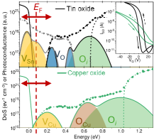
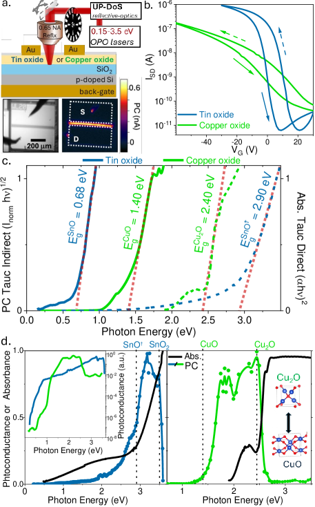
Figure 1a shows the cross section of tin and copper oxide TFTs with their associated photoconduction (PC) microscopy map in the lower panel. The measured transfer curves (W/L = 10, VSD = 1 V) shown in Fig. 1b of tin oxide and copper oxide TFTs both show characteristic p-mode behavior with a negative gate voltage turn-on and 105 and 104 on-to-off ratios, respectively. Clockwise hysteresis due to hole trapping and re-emission is pronounced for both types of TFTs. Figure 1c presents indirect Tauc-like plots of normalized TFT photoconductance [ versus h] that are shown as solid lines. For tin oxide, the estimated indirect bandgap is equal to 0.68 eV, corresponding to SnO, in good agreement with reported values for SnO of 0.70-0.75 eV. 32, 33 For copper oxide, the estimated indirect bandgap is found to be 1.4 eV, corresponding to CuO. Direct Tauc plots [( versus h] are also shown in Fig. 2a and are indicated as dashed lines. A direct bandgap of 2.9 eV is found for tin oxide, corresponding to SnO, while a direct bandgap of 2.4 eV is estimated for copper oxide, consistent with Cu2O. Table 1 summarizes the bandgaps retrieved from photoconduction and absorption measurements, along with their comparisons of DFT calculated values reported in the literature.
| DoS | Assigned | Peak Energy | FWHM | Peak DoS | DFT Formation | DFT Peak |
|---|---|---|---|---|---|---|
| Peak | Defect | (eV) | (meV) | Energy38 (eV) | Energy38 (eV) | |
| 1 | V+H | |||||
| 2 | V | |||||
| 3 | V | |||||
| 4 | HO | |||||
| 5 | Oi | 0.66 | 63 | 39.2 | 1.1 |
Figure 1d shows a comparison of absorption (black) and photoconductance (blue for tin oxide; green for copper oxide). Abrupt thresholds in which absorption increases while photoconductance decreases of 3.5 eV for tin oxide and 2.4 eV for copper oxide provide strong evidence for the presence of SnO2 and Cu2O, respectively. The inset of Fig. 1d further shows the total raw photoconductance spectrum drops off by a factor of 105 for tin oxide and 107 for copper oxide, as subgap defect states are photoexcited below the respective indirect bandgaps of SnO and CuO.
Taken together, Figs. 1c and 1d provide strong evidence that both the tin oxide and copper oxide thin-films are mixed-phase systems corresponding to SnO SnO2 and CuO Cu2O, respectively. Since XRD characterization shows no evidence of SnO2 and CuO in these thin-films, we conclude that CuO and SnO2 are minority phases compared to Cu2O and SnO.39, 40 For copper oxide, the measured Hall mobility ( 20 cm2/Vs) is consistent with Cu2O while the measured field-effect mobility ( 0.1 cm2/Vs) is most likely due to CuO. Similar mobility properties have been widely reported in the literature. 41, 42, 43 As TFT photoconductance is primarily sensitive to the charge accumulation layer, this supports that the Cu2O-SiO2 (semiconductor-dielectric) interface is heavily oxidized to CuO. 44 45
II.1 Ambipolar SnO Subgap DoS
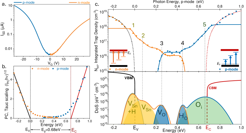
Figure 2a plots the ambipolar SnO TFT transfer curve, and delineates the p-mode and n-mode conduction region where the UP-DoS spectra will be taken. The SnO bandgap is identified in Fig. 2b by applying Tauc scaling to the raw signal. The extracted bandgap of eV is in good agreement with previously reported 0.70-0.75 eV SnO bandgaps.32, 33 Figure 2c (upper panel) plots the integrated trap density, N, for p-mode (blue line, V V) and n-mode (orange line, V V) operation. N is directly proportional to measured TFT photoconductance, and the subgap region consists of a sequence of step-wise features, where each step corresponds to a Gaussian peak in the subgap DoS shown by the dashed lines connected to the lower panel. Each subgap step in N is analytically fit to an error (erf) function (solid line). The above-bandgap response is fit to an indirect absorption lineshape function (dashed lines) accounting for valence band to conduction band transitions. Note that plotting both the p-mode and n-mode signal on the same energy axis requires that the n-mode energy axis be shifted by , where (VBM = 0) is the energy-axis of p-mode, and (CBM = 0) is the energy axis of n-mode.
Figure 2c (lower panel) plots the SnO subgap DoS across the full bandgap. This is quite extraordinary since all prior UP-DoS measurements were conducted using unipolar semiconductors, where measuring the critical subgap states within a few kbT to the active band edge was not possible. Note that the DoS shown in the lower panel of Figure 2c is obtained by differentiating upper panel data, i.e., DoS = . Since each step in the Ntot data is fit to an erf, each Ntot step yields a corresponding Gaussian in the DoS plot. The use of error function fitting prior to differentiating significantly improves the DoS signal-to-noise ratio compared to simple point-by-point numerical differentiation of the raw Ntot data. Table 2 summarizes the parameters of each subgap DoS peak, numbered 1-5.
The identities of SnO subgap peaks 1-5 in Fig. 2c are ascribed by comparison to the DFT calculations of Varley et al..38 Subgap peaks in SnO are assigned as: 1. tin vacancy + hydrogen defect (V, acceptor), 2. tin vacancy (V, acceptor), 3. oxygen vacancy (V, donor), 4. hydrogen on an oxygen site (H, donor) and 5. oxygen interstitial (Oi, acceptor). While the tin and oxygen vacancy peaks are expected, peaks 1 and 5 require more discussion.
Figure 2c shows peak 1 is observed in both n- and p-mode UP-DoS measurements at a photon energy eV above the bandgap. Thus, in principle, peak 1 could be positioned eV below EV or above EC. Since peak 1 is observed to have the largest density of all peaks, it is assigned to the defect with the lowest formation energy, VSn+H located at the VB edge, as identified by Varley et al.
Varley et al. calculates a hydrogen interstitial donor defect with transition energy of eV from the valence band maximum,38 which could potentially correspond to peak 5 measured at eV from the valence band maximum. However, from charge balance considerations, peak 5 needs to be a neutral acceptor rather than a positively charged ionized donor. Therefore, we propose an oxygen interstitial Oi acceptor as an alternative identification for this peak. While DFT studies calculate a low formation energy for this defect, they also predict a transition energy above the bandgap rather than near the conduction band minimum. 25, 38, 24, 46 In part owing to the coplanar structure of the SnO lattice layers, oxygen interstitial are suspected to be abundant in SnO, and function as an intermediary species in the oxidation of SnO to SnO2. 46, 47
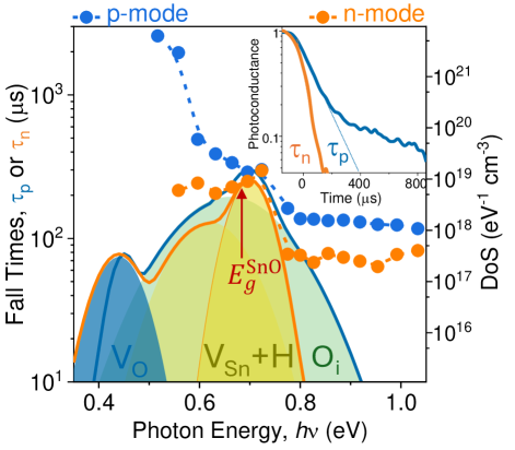
Figure 3 shows TFT fall times, changes for each successive peak in the overlaid SnO DoS until plateauing for above gap photoexcitations at 130 s in p-mode (blue line) and 70s in n-mode (orange line). Interestingly, near eV, both n- and p-mode fall times merge to match at 280 s, suggesting both photoexcitions are dominated by relaxation from the same band-edge defect site. This matching abrupt increase in both fall times in Fig. 3, independently confirms the strong carrier trapping nature of the corresponding V+H acceptor DoS band-edge peak that is overlaid from Fig. 2c. Exploring midgap photoexcitations down to 0.5 eV, the extracted SnO TFT fall time increases tenfold to 2.5 ms at p-mode gate voltages. To help explain, previous UP-DoS fall time studies by Vogt et al. show charge-neutral defect states have inherently longer fall times than ionized defects from weaker coulombic interactions.5 Accordingly, such p-mode mid-gap photoexcitations are consistent with empty deep donors being photoexcited similar to V to create a neutral filled donor with the expectedly slower 2.5 ms recombination time observed.
II.2 p-type SnO Subgap DoS
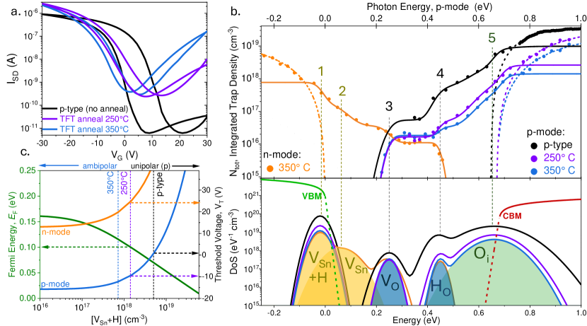
Figure 4 shows the evolution of the SnO subgap DoS from p-mode to ambipolar TFT behavior. In Fig. 4a three SnO TFT transfer curves (W/L = 10, = 1 V) are classified as p-type (black), weak-ambipolar (250 ∘C annealed, purple), and strong-ambipolar (350 ∘C annealed, blue). The corresponding integrated trap densities, Ntot, are shown in Fig. 4b (upper panel). Using orange circles, just one example of a n-mode Ntot spectrum is plotted in Fig. 4b (upper panel) corresponding to the most clearly ambipolar TFT in 4a (blue) . Indicated by the vertical dashed lines, Fig. 4b (upper panel) shows five subgap steps labeled 1–5 that correspond to Gaussian DoS peaks shown in Fig. 4b (lower panel). The peaks observed and their identifications match those previously discussed in Fig. 2.
The lower panel of Fig. 4b further shows that as SnO changes with annealing conditions from p-type to ambipolar behavior, a corresponding decrease in subgap defect density is observed. The significant enhancement in n-mode behavior with annealing that is observed in Fig. 4a is attributed primarily to a decrease of the defect peak located just below the conduction band minimum, identified as Oi. Note that for n-mode operation, Oi behaves as an electron trap.48 To achieve unipolar p-type SnO TFT operation with low off current, similar to black curve of 4a, [Oi] should be sufficiently large to suppress the undesired n-mode behavior.
Figure 4c presents a simulation of the Fermi level energy together with the p- and n-mode threshold voltages as a function of [VSn+H]. The dashed vertical lines indicate the measured concentration of each TFT, whereas the horizontal dashed arrows are visual aids to guide each simulated parameter to the correct y-axis. When cm-3 (as observed for all three TFTs), the simulation shows that [VSn+H] controls the Fermi energy, and consequently the threshold voltage, whereas to a good approximation ]. Furthermore, Fig. 4c shows that at , both n- and p-mode threshold voltages are easily accessible, enabling ambipolar TFT behavior.
II.3 SnO TFT DoS Stability Study
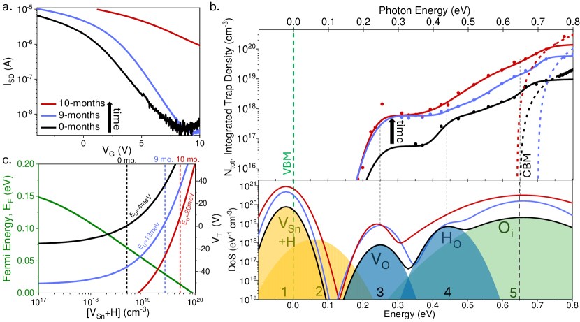
SnO TFT properties change after 0-, 9-, and 10-months of vacuum storage, with a 1-week exposure to lab atmosphere introduced between months 9 and 10. As indicated in Fig. 5a, the threshold voltage exhibits a large positive shift from 1 V (black), to 3 V (blue), and finally to 8 V (red). Furthermore, the off current further increased dramatically from 0.01 A at 9-months to A at 10-months. Similarly, with increasing time Fig. 5b shows a substantial increase in the measured Ntot (upper panel) with a corresponding increase of subgap DoS (lower panel). After 10 months, the resulting large increase in the subgap DoS near Peaks 1 suggests the TFT has become so strongly p-type doped that turn-off is unfeasible, as seen in the associated transfer red curve shown in Fig. 5a.
Figure 5c plots the simulated Fermi level energy and p-mode threshold voltage as a function of increasing concentration of tin-vacancy related states, [V+H]. Previously, in the Fig. 4c simulation, the valence band Urbach energy extracted was constant at E meV over the three different TFT processing conditions. However, the extracted Urbach energy increases in Fig. 5c with the subgap density from E meV at 0 months to E meV at 9 months, and finally to E meV after 10 months of vacuum storage.
Since the valence band Urbach energy is a measure of disorder on the anion sublattice, it is reasonable that there may be some correlation between certain subgap peaks and valence band tail states. The observed increase in [V+H] with increasing vacuum storage time is likely associated with the oxidative process, SnO SnO2 since this process is known to be associated with tin vacancy formation. 49, 50 However, it is also possible that hydrogen incorporation or diffusion could also play a role in SnO TFT degradation.
II.4 Copper Oxide Subgap DoS
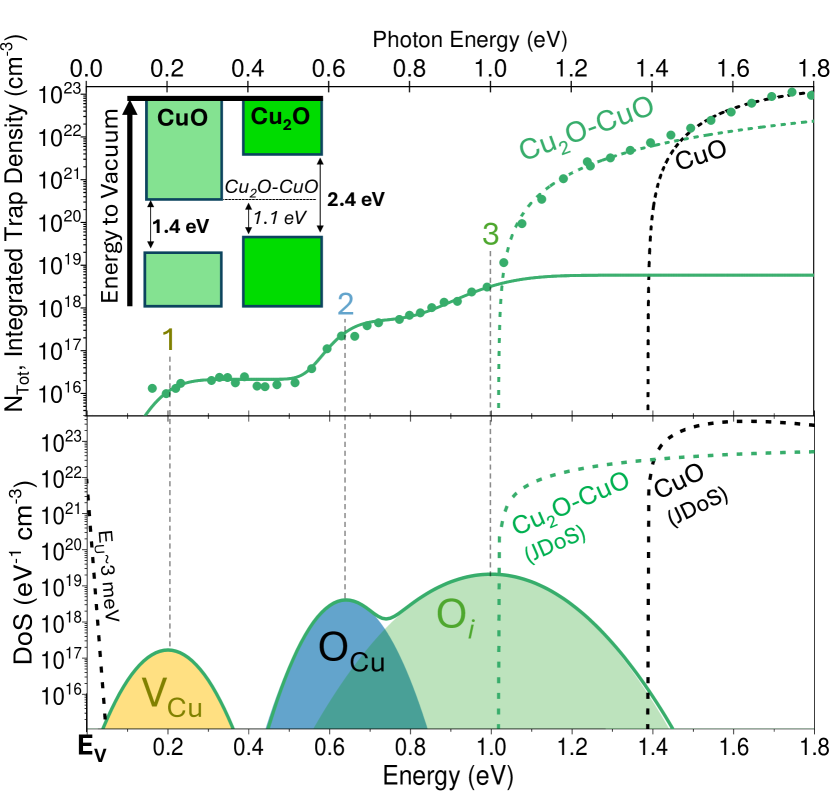
The copper oxide TFT transfer curve is unipolar p-type with a 104 turn-on, as shown previously in Fig. 1b. Figure 6 presents the associated subgap integrated trap density, Ntot in the top panel, and density of states, DoS in the bottom panel. Three Ntot clear steps labeled 1-3 are indicated in Fig. 6 along with three corresponding Gaussian DoS peaks positioned at 0.20, 0.64, and 1.00 eV above the valence band maximum. Proposed defect identifications for these three peaks are labeled in Fig. 6 and summarized in Table III.
Proposed peak identifications of the three copper oxide peaks measured are based on DFT calculations by Zivković and de Leeuw, or by Scanlon et al., for CuO or Cu2O defect site and formation energies. 27, 28 The measured 0.20 eV peak is identified as a copper vacancy acceptor, V, comparable to the 0.17 eV value estimate for CuO or the 0.23 eV estimate for Cu2O. The measured 0.64 eV peak is ascribed to an oxygen-on-copper antisite defect, O, similar to the calculated value of 0.49 eV on the CuO sublattice. 27 Finally, the peak measured at 1.00 eV is ascribed to an oxygen interstitial, Oi, since both phases are calculated to have Oi point defects in this portion of the bandgap with predicted ionization energies of 1.14 eV and 1.08 eV for CuO and Cu2O, respectively.27, 28 Note that the Oi defect in copper oxide, as shown in Fig. 6, has a similar Gaussian width and position within the subgap as the Oi defect in tin oxide, as shown in Fig. 2.
Similar to tin oxide, the measured copper oxide subgap DoS is used to estimate the Fermi level energy and valence band Urbach energy to be EF = 260 meV and EU = 3 meV, respectively. Then, from charge balance, the copper oxide equilibrium hole concentration is estimated to be , which is approximately equal to the copper vacancy concentration [VCu].
| DoS | Assigned | Peak Energy | FWHM | Peak DoS | DFT Formation | DFT Peak |
|---|---|---|---|---|---|---|
| Peak | Defect | (eV) | (meV) | Energy27 (eV) | Energy27 (eV) | |
| 1 | V | |||||
| 2 | O | |||||
| 3 | Oi | 210 | 0.3 |
Recall from Fig. 1c that the indirect bandgap of copper oxide was estimated to be 1.4 eV – equal to that of CuO – based on a linear-regression fit to a Tauc-like plot of normalized photoconductance. However, note that this indirect bandgap estimate is based on ignoring a weaker subgap absorption response with a lower-energy threshold of 1.1 eV (see Fig. 2a). If this weaker subgap absorption response is taken into account, as indicated in Fig. 6, it can only be included as an above-bandgap feature (in which the DoS is given by a quadratic function of energy), rather than a below-bandgap feature (in which the DoS is described by a Gaussian function of energy). This suggests that the indirect bandgap of copper oxide is actually equal to 1.1 eV rather than 1.4 eV, as expected for CuO.
How do we rationalize the physics of this 1.1 eV lower-energy threshold since it appears to be inconsistent with both CuO and Cu2O? We propose that this 1.1 eV lower-energy threshold is a mixed-phase transition involving real-space electron transfer in which a filled initial electronic state at the Cu2O valence band maximum is excited into an empty final electronic state at the CuO conduction band minimum. Such a process is accomplished by real-space electron transfer from the Cu2O (filled) initial state into the CuO (empty) final state, and is labeled in Fig. 6 as a Cu2O-CuO (mixed phase) transition. Khoo et al. estimate the energy difference from the Cu2O valence band to the CuO conduction band to be 1.09 eV, in good agreement with our observed 1.1 eV threshold energy. 36 Figure 6 inset shows the estimated energy band alignment for the mixed-phase copper oxide.
II.5 Unpassivated and Passivated Copper Oxide Subgap DoS
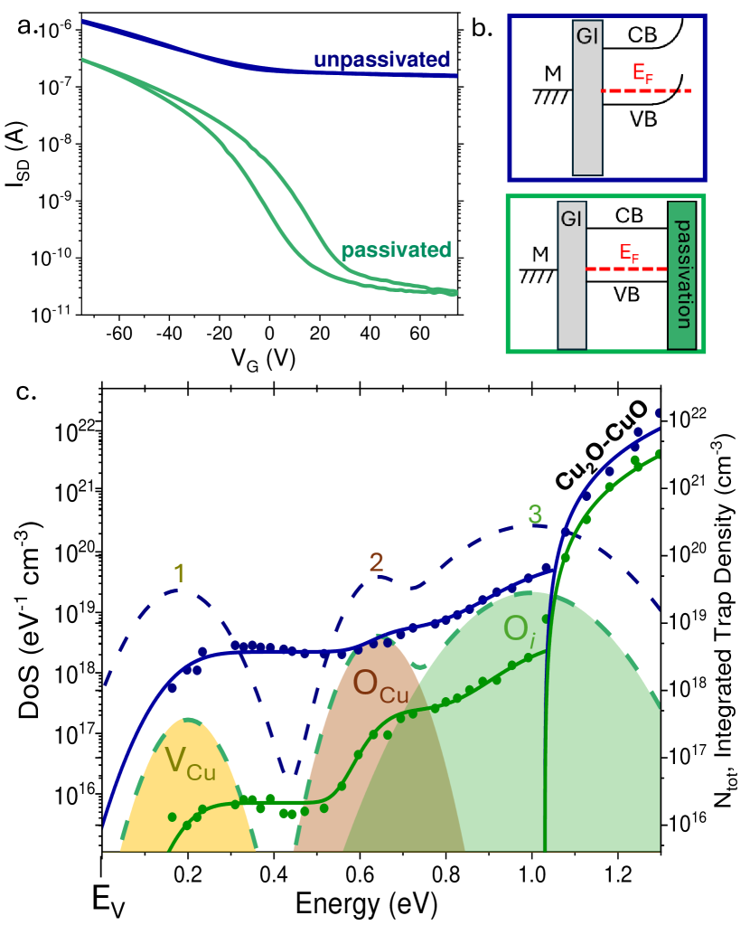
Figure 7a compares the transfer curves of copper oxide TFTs when the back-channel is passivated (green) or unpassivated (blue). The unpassivated device has a high off current and no clear turn-off voltage. Figure 7b illustrates energy band diagrams showing the existence of a backside accumulation layer responsible for the poor performance exhibited by the unpassivated TFT. In contrast, passivation eliminates the back-side accumulation layer and its deleterious effect upon TFT performance. Figure 7c presents a comparison of Ntot and DoS for an unpassivated and passivated copper oxide TFT. Consistent with prior studies, the degraded performance of the unpassivated TFT appears to correlate with the enhanced defect DoS across the entire subgap. 51 This result suggests that an increase in charged copper vacancies at the backside may be responsible for the formation of this additional accumulation layer.
III Conclusions
Tin oxide and copper oxide constitute two possible material strategies for realizing p-type oxide TFTs. For each TFT, the subgap integrated trap density is measured over a tunable 0.15 - 3.5 eV laser excitation range using the ultrabroadband photoconduction DoS (UP-DoS) technique.5, 52, 6 The below-gap photoconductivity drops off by 105 in tin oxide and 107 in copper oxide and indicates how the corresponding SnO and CuO material phases drive p-type conductivity in each TFT.
Measuring subgap integrated traps in n-mode and p-mode for ambipolar TFTs provides two complimentary DoS spectra that fully span the subgap. In tin oxide, the resulting subgap DoS shows five subgap peaks assigned as: tin vacancies (V and V+H), oxygen vacancies in the midgap (V and H), and oxygen interstitial sites. The near VB-edge tin vacancy V+H peak largely determines the TFT equilibrium Fermi level energy and p-doping, such that . Adjacent to the CB-edge, the broad oxygen interstitial peak density suppresses n-mode conduction to achieve the desired unipolar p-mode TFT behavior with low off current.
For p-type copper oxide TFTs, the subgap DoS shows just three subgap peaks assigned as: copper vacancies near the VB-edge, oxygen-on-copper antisites in the mid-gap, and oxygen interstitial sites near the CB-edge. Similar to the tin oxide case, the metal vacancy peak, V, determines the TFT p-doping, such that . Copper oxide thin-film formation tends to favor the formation of Cu2O, a wider bandgap p-type semiconductor with some inadvertent incorporation of CuO, a narrow bandgap p-type semiconductor with a poor mobility. Even though the oxidized CuO is likely only prevalent near the semiconductor-dielectric interface, its lower bandgap is likely responsible for the low field-effect mobility in the copper oxide TFTs. Synthesis of a phase-pure Cu2O thin-film appears to be a challenging but desirable goal.
IV Experimental Section
1. p-type TFT preparation
Bottom gate, top contact TFTs were fabricated with a thermally-grown SiO2 (thickness, nm) as the gate dielectric and heavily-doped p-type Si (100) substrate as the gate electrode. Thermally evaporated gold ( nm) was used as the source and drain contacts. The channel layer and the contacts were patterned by photolithography with either lift-off or wet etching method. Unless otherwise stated, the back channel was passivated with Al2O3 ( nm) by atomic layer deposition (ALD) in all devices. For a width-to-length ratio (W/L) of 10, the TFTs reported have a channel width and length of 1000 m and 100 m.
The Cu2O channel layer ( nm) was deposited in a high target utilization sputtering system from a metallic target. 40 A post deposition annealing was performed at 700 ∘C after the channel patterning. The unpassivated Cu2O TFT exhibits a field effect mobility, of 0.21 cm2V-1s-1 with a small on-off ratio . In the passivated device, the on-off ratio increases significantly to but with a reduced on-state current, thus of 0.07 cm.
The SnO channel layer was deposited by ALD using Sn(II) bis-(tert-butoxide) and water at a substrate temperature of 170 ∘C.39 By varying SnO thickness and process conditions, TFTs exhibit either depletion mode (for TFTs, D1 and D2) or enhancement modes (E1 and E2), as shown in Supporting Table S.I. TFTs incorporating a thicker SnO layer are expected to have a high carrier concentration (D1 and D2), therefore the device operates in depletion mode and the current conduction (mobility) depends on the annealing temperatures. On the other hand, devices E1 and E2 incorporate a more resistive and thinner SnO layer, thus requiring two annealing steps. Even though the is similar, E2 with a higher TFT annealing temperature exhibits ambipolar properties, while E1 with a lower TFT annealing temperature exhibits predominantly p-type characteristics.
Post-growth analysis suggests that Cu2O and SnO should be the dominant materials present in each TFT.40, 39 However, the active channel is known to readily oxidize to CuO and SnO2.53, 54 Before measurements, the absorption spectra (Cary UV-Vis-IR) for tin and copper oxide thin-films derived from the TFT growths are compared to the corresponding TFT photoconduction(PC) spectra.
2. TFT Ultrabroadband Photoconductance DoS Microscopy
The Ultrabroadband Photoconduction Density of States (or UP-DoS) microscopy method is applied to tin and copper oxide TFTs to measure the subgap defects density.5, 52, 6 Figure 1a depicts the UP-DoS setup measuring the photoconduction, on a TFT with an ultrabroadband tunable laser from photon energies of 0.15 to 3.5 eV. The diffraction-limited laser illuminates a tin or copper oxide active channel from the top side through the thin passivation layer of aluminum oxide. The TFT gate voltage is carefully selected to ensure that the TFT transfer curve is a quasi-linear regime, such that the small incident photon flux ( photons/cm2) induces a small linear shift in the illuminated transfer curve.5 The TFT conductivity is continuously monitored with a custom-built RF probe microscopy station that uses all-reflective 4f-scanning optics. A high-NA (0.45) 52x reflective objective delivers a nearly diffraction-limited tunable-laser. The bottom panel of Figure 1a shows this 1.1 eV laser mapping the TFT response over the copper oxide TFT active region.
To measure the DoS of a TFT, the primary observable is the photon-normalized photoconduction, , where IPC is the Zurich lock-in amplifier (HFLI) detected photoconduction signal and is the incident laser power (ranges from 0.1 to 100 W). I has units of AeV-1W-1. Providing , only band-to-defect (p-mode) or defect-to-band (n-mode) transitions are likely, and the detected signal can be approximated as,
| (1) | |||
| (2) |
where is the subgap DoS of empty defect states excited to with photon energy from filled valence band states, , in p-mode operation. is the subgap DoS of filled defect states that are excited to empty conduction band states, , in n-mode operation. See Supporting Information Section I for a comparison when .
To obtain the absolute integrated total defect density per unit volume, , the directly measure quantity I must be simply rescaled by a constant given in the bracketed expression below,5
| (3) |
where is the gate oxide capacitance of the TFT, is the charge of the electron, is the thickness of the excited accumulation channel ( 0.3 nm). is the non-illuminated slope of the TFT transfer curve in the linear regime where the UP-DoS measurement was conducted. is the rate of incident photons that causes the signal to saturate owing to state filling (or ). Finally, the first derivative of Eqn. 3 with respect to energy provides the desired experimental subgap DoS as .
3. Charge Balance and Discrete Trap Model
By using the full functional form of all measured subgap DoS peaks, it is possible to use a discrete trap model together with charge balance to calculate the equilibrium Fermi energy and Urbach energies. The equation for charge balance involves a balance between positive and negative charge,
| (4) |
where () is ionized Gaussian donors, () is ionized valence band tail donors, () is filled Gaussian acceptors, and is free electron/hole density (see Supporting Information Section II for full functional form). The equation for the discrete acceptor trap model is: 55
| (5) |
where is electron charge, and is the gate insulator capacitance density. Note that the only two parameters not measured by UP-DoS in Eq. 4 and Eq. 5 are the fermi level energy, EF, and the valence band tail donors ( or ), whereas ( or ) further only depends on EF, the hole effective mass m, and valence band Urbach energy EU. 19 By using literature-reported values of m, 56, 57, 58 the system of equations can be solved for the two unknowns, EF and EU. Similarly, by instead using the discrete trap donor model,55 the conduction band Urbach energy can be estimated. Finally, when EU is known, using the equations above, it is possible to simulate the Fermi level energy together with n- and p-mode threshold voltages as a function of hypothetical change in defect concentrations.
Supporting Information
Details on sample characteristics and optical conductivity data modeling methods.
Acknowledgments
This work is supported by a SAMSUNG Global Research Outreach (GRO) Award. KMN and AJF acknowledge support from EPSRC EP/X025195/1, ‘Innovative Material, Processes, and Devices for Low Power Flexible Electronics: Creating a Sustainable Internet of Everything.’
Data Availability Statement: The data that support the findings of this study are available from the corresponding author upon request.
References
- [1] A. Nathan, S. Lee, S. Jeon, J. Robertson, Journal of Display Technology 2014, 10, 11 917.
- [2] G. Wakimura, Y. Yamauchi, Y. Kamakura, Journal of Advanced Simulation in Science and Engineering 2015, 2, 1 201.
- [3] J. F. Wager, B. Yeh, R. L. Hoffman, D. A. Keszler, Current Opinion in Solid State and Materials Science 2014, 18, 2 53.
- [4] H. Hosono, Nature Electronics 2018, 1, 7 428.
- [5] K. T. Vogt, C. E. Malmberg, J. C. Buchanan, G. W. Mattson, G. M. Brandt, D. B. Fast, P. H.-Y. Cheong, J. F. Wager, M. W. Graham, Physical Review Research 2020, 2, 3 033358.
- [6] G. W. Mattson, K. T. Vogt, J. F. Wager, M. W. Graham, Advanced Functional Materials 2023, 33, 25 2300742.
- [7] Z. Wang, P. K. Nayak, J. A. Caraveo-Frescas, H. N. Alshareef, Advanced Materials 2016, 28, 20 3831.
- [8] Z. Ouyang, W. Wang, M. Dai, B. Zhang, J. Gong, M. Li, L. Qin, H. Sun, Materials 2022, 15, 14 4781.
- [9] N. Devabharathi, S. Yadav, I. Dönges, V. Trouillet, J. J. Schneider, Advanced Materials Interfaces 2024, 11, 16 2301082.
- [10] W. Xu, J. Zhang, Y. Li, L. Zhang, L. Chen, D. Zhu, P. Cao, W. Liu, S. Han, X. Liu, et al., Journal of Alloys and Compounds 2019, 806 40.
- [11] J. H. Lee, J. Kim, M. Jin, H.-J. Na, H. Lee, C. Im, Y. S. Kim, ACS Applied Electronic Materials 2023, 5, 2 1123.
- [12] E. Fortunato, R. Barros, P. Barquinha, V. Figueiredo, S.-H. K. Park, C.-S. Hwang, R. Martins, Applied Physics Letters 2010, 97, 5.
- [13] Y. Ogo, H. Hiramatsu, K. Nomura, H. Yanagi, T. Kamiya, M. Hirano, H. Hosono, Applied Physics Letters 2008, 93, 3.
- [14] L. Lan, J. Peng, IEEE Transactions on Electron Devices 2011, 58, 5 1452.
- [15] K. Nomura, H. Ohta, A. Takagi, T. Kamiya, M. Hirano, H. Hosono, Nature 2004, 432, 7016 488.
- [16] Y. Jang, J. Park, J. Kang, S.-Y. Lee, ACS Applied Electronic Materials 2022, 4, 4 1427.
- [17] A. Belmonte, H. Oh, S. Subhechha, N. Rassoul, H. Hody, H. Dekkers, R. Delhougne, L. Ricotti, K. Banerjee, A. Chasin, et al., In 2021 IEEE International Electron Devices Meeting (IEDM). IEEE, 2021 10–6.
- [18] K. Iordanidou, C. Persson, Materials Science in Semiconductor Processing 2021, 121 105297.
- [19] J. F. Wager, AIP Advances 2017, 7, 12.
- [20] Y. Hu, D. Schlom, S. Datta, K. Cho, ACS Applied Materials & Interfaces 2022, 14, 22 25670.
- [21] Y. Wang, S. Lany, J. Ghanbaja, Y. Fagot-Revurat, Y. P. Chen, F. Soldera, D. Horwat, F. Mücklich, J. Pierson, Physical Review B 2016, 94, 24 245418.
- [22] E. Fortunato, V. Figueiredo, P. Barquinha, E. Elamurugu, R. Barros, G. Gonçalves, S.-H. K. Park, C.-S. Hwang, R. Martins, Applied Physics Letters 2010, 96, 19.
- [23] A. Sekkat, V. H. Nguyen, C. A. Masse de La Huerta, L. Rapenne, D. Bellet, A. Kaminski-Cachopo, G. Chichignoud, D. Muñoz-Rojas, Communications Materials 2021, 2, 1 78.
- [24] A. Togo, F. Oba, I. Tanaka, K. Tatsumi, Physical Review B 2006, 74, 19 195128.
- [25] A. W. Lee, D. Le, K. Matsuzaki, K. Nomura, ACS Applied Electronic Materials 2020, 2, 4 1162.
- [26] J. P. Allen, D. O. Scanlon, L. F. Piper, G. W. Watson, Journal of Materials Chemistry C 2013, 1, 48 8194.
- [27] A. Zivković, N. H. de Leeuw, Physical Review Materials 2020, 4, 7 074606.
- [28] D. O. Scanlon, B. J. Morgan, G. W. Watson, A. Walsh, Physical Review Letters 2009, 103, 9 096405.
- [29] A. W. Lee, Y. Zhang, C.-H. Huang, K. Matsuzaki, K. Nomura, Advanced Electronic Materials 2020, 6, 12 2000742.
- [30] C.-Y. Jeong, D. Lee, Y.-J. Han, Y.-J. Choi, H.-I. Kwon, Semiconductor Science and Technology 2015, 30, 8 085004.
- [31] H. Luo, L. Liang, H. Cao, M. Dai, Y. Lu, M. Wang, ACS Applied Materials & Interfaces 2015, 7, 31 17023.
- [32] Y. Wu, Z. Tang, G. J. Cruz, Y. Yang, W. Zhang, W. Ren, P. Zhang, Physical Review B 2022, 106, 8 085201.
- [33] K. J. Saji, Y. V. Subbaiah, K. Tian, A. Tiwari, Thin Solid Films 2016, 605 193.
- [34] W. Guo, L. Fu, Y. Zhang, K. Zhang, L. Liang, Z. Liu, H. Cao, X. Pan, Applied Physics Letters 2010, 96, 4.
- [35] W. Zhou, Y. Liu, Y. Yang, P. Wu, The Journal of Physical Chemistry C 2014, 118, 12 6448.
- [36] P. Khoo, K. Satou, M. Izaki, In IOP Conference Series: Materials Science and Engineering, volume 920. IOP Publishing, 2020 012028.
- [37] D. Ozaslan, O. Erken, M. Gunes, C. Gumus, Physica B: Condensed Matter 2020, 580 411922.
- [38] J. Varley, A. Schleife, A. Janotti, C. Van de Walle, Applied Physics Letters 2013, 103, 8.
- [39] D. E. Gomersall, K. M. Niang, J. D. Parish, Z. Sun, A. L. Johnson, J. L. MacManus-Driscoll, A. J. Flewitt, Journal of Materials Chemistry C 2023, 11, 17 5740.
- [40] S. Han, K. M. Niang, G. Rughoobur, A. J. Flewitt, Applied Physics Letters 2016, 109, 17.
- [41] J. Jo, J. D. Lenef, K. Mashooq, O. Trejo, N. P. Dasgupta, R. L. Peterson, IEEE Transactions on Electron Devices 2020, 67, 12 5557.
- [42] L. Guo, M. Zhao, D.-M. Zhuang, M. Cao, L. Ouyang, X. Li, R. Sun, Z. Gao, Applied Surface Science 2015, 359 36.
- [43] V. Singh, J. Sinha, S. Shivashankar, S. Avasthi, Journal of Materials Chemistry C 2023, 11, 22 7356.
- [44] S. Im, Y.-G. Chang, J. H. Kim, Photo-Excited Charge Collection Spectroscopy: Probing the traps in field-effect transistors, Springer Science & Business Media, 2014.
- [45] F.-Y. Ran, M. Taniguti, H. Hosono, T. Kamiya, Journal of Display Technology 2015, 11, 9 720.
- [46] F. Oba, M. Choi, A. Togo, A. Seko, I. Tanaka, Journal of Physics: Condensed Matter 2010, 22, 38 384211.
- [47] M. Januar, C.-Y. Lu, H.-C. Lin, T.-Y. Huang, C.-M. Yang, K.-K. Liu, K.-C. Liu, Materials Advances 2024, 5, 11 4679.
- [48] J. F. Wager, Amorphous Oxide Semiconductors: IGZO and Related Materials for Display and Memory 2022, 105–123.
- [49] T. Leijtens, R. Prasanna, A. Gold-Parker, M. F. Toney, M. D. McGehee, ACS Energy Letters 2017, 2, 9 2159.
- [50] F. Hao, C. C. Stoumpos, D. H. Cao, R. P. Chang, M. G. Kanatzidis, Nature Photonics 2014, 8, 6 489.
- [51] M. Napari, T. N. Huq, D. J. Meeth, M. J. Heikkilä, K. M. Niang, H. Wang, T. Iivonen, H. Wang, M. Leskela, M. Ritala, et al., ACS Applied Materials & Interfaces 2021, 13, 3 4156.
- [52] G. W. Mattson, K. T. Vogt, J. F. Wager, M. W. Graham, Journal of Applied Physics 2022, 131, 10 105701.
- [53] Y. Alajlani, F. Placido, A. Barlow, H. O. Chu, S. Song, S. U. Rahman, R. De Bold, D. Gibson, Vacuum 2017, 144 217.
- [54] C. K. G. Kwok, Y. Wang, X. Shu, K. M. Yu, Applied Surface Science 2023, 627 157295.
- [55] D. Hong, G. Yerubandi, H. Chiang, M. Spiegelberg, J. Wager, Critical Reviews in Solid State and Materials Sciences 2008, 33, 2 101.
- [56] Y. Ogo, H. Hiramatsu, K. Nomura, H. Yanagi, T. Kamiya, M. Kimura, M. Hirano, H. Hosono, physica status solidi (a) 2009, 206, 9 2187.
- [57] F. Koffyberg, F. Benko, Journal of Applied Physics 1982, 53, 2 1173.
- [58] J. Hodby, T. Jenkins, C. Schwab, H. Tamura, D. Trivich, Journal of Physics C: Solid State Physics 1976, 9, 8 1429.
Table of Contents