Correlated Structural and Optical Characterization of Hexagonal Boron Nitride
Abstract
Hexagonal boron nitride (hBN) hosts quantum emitters that exhibit single-photon emission and spin-dependent fluorescence at room temperature. These features make hBN a promising platform for quantum sensing and photonics. Despite many investigations of their optical properties, the emitters’ chemical structure remains unclear, as does the role of contamination at surfaces and interfaces in forming the emitters or modifying their properties. We prepare hBN samples that are compatible with both confocal photoluminescence microscopy (PL) and transmission electron microscopy (TEM), and we use those techniques to investigate correlations between fluorescent emission, flake morphology, and surface residue. We find that the microscopy techniques themselves induce changes in hBN’s optical activity and residue morphology: PL measurements induce photobleaching, whereas TEM measurements alter surface residue and emission characteristics. We also study the effects of common treatments — annealing and oxygen plasma cleaning — on the structure and optical activity of hBN. The results illustrate the power and importance of correlative studies to elucidate aspects of microscopic mechanisms that influence hBN’s functionality as a host for quantum emitters and spin defects.
I Introduction
Hexagonal boron nitride (hBN) is a van der Waals material with utility across many applications. For example, given that hBN is a wide-bandgap semiconductor (5.9 eV) [1, 2], it is frequently used as an insulating layer in electronic devices [3, 4, 5]. More recently, hBN has emerged as an exciting candidate for use in quantum information technologies, as the material hosts bright quantum emitters at room temperature [6, 7, 8, 9]. Some of these emitters display spin-dependent properties and may therefore be utilized as spin qubits [10, 11, 12, 13, 14]. However, these quantum emitters are not yet fully understood. Identifying emitters is particularly complex because they are sensitive to interfaces with other materials [7, 15] and local environmental effects (e.g., defects [11], strain [16, 17], and contamination [18, 19]), which are especially pertinent concerns when utilizing any 2D material. Understanding and controlling the properties of hBN, particularly at its surface, are therefore crucial to advancing quantum information and photonics applications.
Techniques such as photoluminescence (PL) microscopy and scanning electron microscopy (SEM) have previously been employed to understand and create quantum emitters in hBN. PL provides valuable information about optical properties, including absorption and emission characteristics, while offering insight into chemical and electronic information [2, 20]. SEM has been used to study surface topography and morphology [7, 8], in addition to activating emission centers in hBN by electron irradiation [6, 21, 22]. More recently, transmission electron microscopy (TEM) has been used as a means of studying quantum emission in hBN when paired with PL or cathodoluminescence spectroscopy [23, 19]. TEMs enable direct observation of material structure down to the atomic level and are generally operated at much higher accelerating voltages than SEMs (80–200 kV versus 5–30 kV), opening up a new regime of irradiation conditions to be explored for the possible creation of emitters [24, 25, 26].
While the optical properties and material structure of hBN are well-studied separately, few studies have investigated them in parallel. The absence of studies employing both TEM and PL microscopy can be partially attributed to the disparity in scale at which these two techniques operate. Confocal PL studies in the visible-wavelength range are typically limited to a resolution of 300 nm, whereas TEM studies can achieve atomic resolution. By combining both of these techniques, the capabilities of TEM can be leveraged to help determine the structural and chemical composition of quantum emitters identified via PL microscopy.
In this study, we combine PL and TEM imaging to bridge the gap in understanding between hBN’s optical properties and material structure. We focus on changes in overall optical activity and flake morphology associated with different measurements and treatments, rather than investigating single-photon emitters with PL or few-atom defects with TEM. To this end, we fabricate custom substrates compatible with both microscopies onto which hBN flakes ranging from 10 to 30 nm thick, as measured by atomic force microscopy (AFM), are transferred. First, we consider the effects of PL and TEM measurements themselves on hBN, which is particularly important because of the iterative approach of the measurements. We show that exposure to the electron beam during TEM imaging induces changes to contaminants present on flakes and that PL imaging induces photobleaching. Then, we demonstrate the utility of this protocol by studying correlated changes in structure and optical activity following annealing and oxygen plasma irradiation, treatments commonly applied to hBN [27, 19, 28, 1, 29, 30]. We find that both treatments significantly alter sample morphology and optical activity. Each sample discussed in this paper received a distinct sequence of measurements and treatments which are summarized in Table S1 in the Supporting Information. The unique procedure introduced here facilitates a comprehensive study of quantum emission in hBN, revealing the detailed and complex interplay between material structure and optical activity and the effects of common treatments. Furthermore, this approach can be easily adapted to other 2D materials, demonstrating its broad utility for advancing the field as a whole.
II Material and Instrumental Considerations
II.1 Sample Requirements
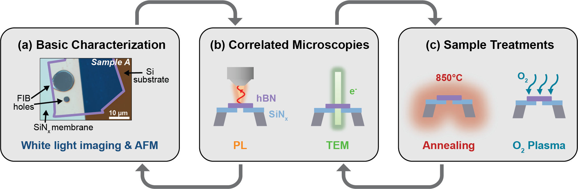
Each sample discussed in this paper received a distinct sequence of measurements and treatments that are summarized in Table S1 in the Supporting Information. Figure reffig:Schematic summarizes the different characterization methods and treatments we explore. Sample preparation begins by mechanically exfoliating flakes of hBN from bulk crystal (HQ Graphene) and using polydimethylsiloxane (PDMS) viscoelastic stamping to transfer flakes onto 100100 m2 silicon nitride (SiNx) windows. To improve TEM resolution and ensure that PL measurements are not subject to substrate induced effects, hBN flakes are suspended over holes patterned in SiNx windows via focused ion beam (FIB) milling. A 5- to 10-m-diameter FIB hole (Fig. 1a) provides a sufficiently large suspended region of material suitable for both TEM and PL microscopy, determined by the diffraction limit of the laser. Smaller, 2-m-diameter FIB holes (Fig. 1a) help define the sample orientation and provide an area over which the TEM can initially be aligned.
Flake thickness is another important consideration. Monolayer or few-layer flakes are best for TEM studies at atomic resolution. However, stable single-photon emitters in hBN tend to occur in thicker flakes that are typically at least 30 nm thick [31, 32]. Therefore, we utilized flakes of intermediate thickness, ranging from 10 nm to 30 nm, to meet the needs of both microscopies. Flakes of the desired thickness were identified by optical contrast prior to transferring and subsequently confirmed with AFM (see Table S1 in the Supporting Information).
II.2 Effects of Observations
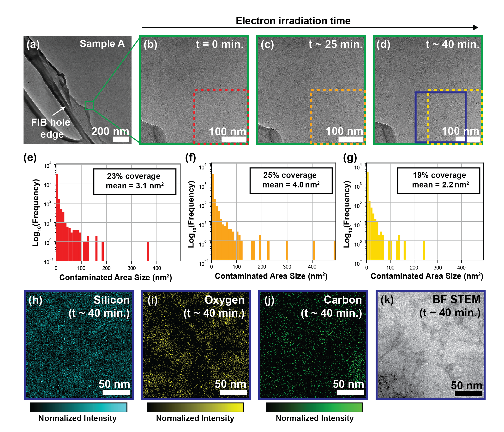
Figure 2 demonstrates the effect of electron beam irradiation on a representative region of Sample A over time. Figure 2b shows that this region of Sample A is covered with a uniform film of residue. However, with prolonged exposure to the electron beam (20 nA probe current), the residue changes in structure and density. Qualitatively, the residue appears to clump together and diminish over time, resulting in the lacey network of residue shown in Figure 2d after 40 minutes of irradiation. Upon analyzing the changes in contamination coverage and distribution of contaminated areas by size, we found that at 0, 25, and 40 minutes, residue coverage was 23%, 25%, and 19%, respectively (see Figs. S2 and S3 in the Supporting Information for a detailed description of this analysis). Histograms of contaminated areas reveal that the average size of contaminated follows a similar trend: average size increases between 0 and 25 minutes, then decreases (Fig. 2e-g). The overall decrease in contamination coverage and average size between 0 and 40 minutes of irradiation shows that prolonged exposure to the electron beam has a cleaning effect, while the increase between 0 and 25 minutes implies that this effect is dose-dependent. It has been shown that hydrocarbons tend to diffuse across the surface of samples towards the electron beam where they are eventually polymerized and fixed in place, often covering features of interest [33, 34]. On the other hand, electron irradiation can also remove material through knock-on damage, radiolysis, or charging effects [35]. These competing phenomena explain the non-monotonic change in residue on Sample A.
The residue shown in Figure 2b-d likely arises from the PDMS used to transfer hBN flakes. A wide body of literature describes how contamination arising from polymer-assisted transfer techniques of 2D materials is a pervasive issue for the field, and hBN is no exception [36, 37, 38, 39]. Energy dispersive x-ray spectroscopy (EDS) maps confirm the presence of silicon, carbon and oxygen species, which is consistent with the composition of PDMS (see Fig. 2h-j and Fig. S1 in the Supporting Information) and previous work [36]. Moreover, all three maps appear to be spatially correlated with the contaminated (dark) areas in the corresponding brightfield scanning TEM (BF STEM) image (Fig. 2k).
In an effort to understand how electron irradiation and changes to surface contaminants impact optical activity, Sample A was also studied with PL microscopy before and after TEM imaging. It is worth noting that the 80kV accelerating voltage used here exceeds the knock-on energies of boron and nitrogen [26, 40, 41, 42]. Therefore when considering the effect of electron irradiation on optical activity, we cannot rule out the possibility that a combination of changes in contamination structure and changes in hBN’s lattice may both play a role.
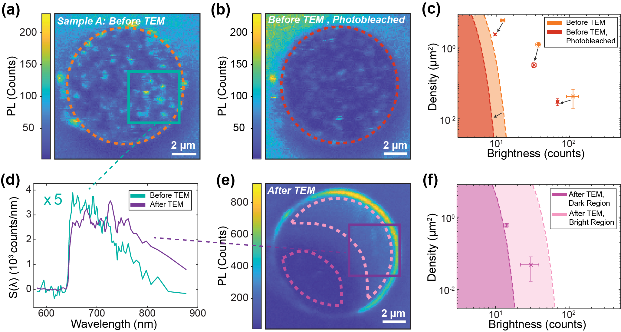
Figure 3 illustrates changes in optical activity due to the PL and TEM characterization techniques themselves. The first PL image of Sample A prior to electron irradiation shows bright localized emission (Fig. 3a). The laser was then rastered over the 1212 m2 area at 100 W for about 20 minutes, followed by 300 W for about 2 minutes. Figure 3b shows that after prolonged laser exposure, emission is still localized but is dimmer within the suspended region. This phenomenon, known as photobleaching, has been previously observed in hBN [19]. A statistical analysis was performed on these data that identifies families of emitters based on their density and brightness (details in Methods). Here, this method is used to quantify changes due to photobleaching. The results indicate a decrease in emitter density and/or brightness following the laser exposure (Fig. 3c).
After photobleaching, Sample A was subject to electron irradiation in the TEM to obtain the images shown in Figure 2b-d (see Table S1 for the sequence of measurements). PL imaging and spectroscopy reveal that electron exposure measurably changes the nature of fluorescent emission. Following the TEM imaging, the upper right portion of the suspended region exhibits diffuse bright emission, whereas the lower left portion—where Sample A was irradiated for 40 minutes—appears significantly dimmer. The brightening and shift to a diffuse morphology is consistent across other TEM-imaged samples in this study (Fig. S7b,e), as well as findings in prior work [26]. The subsequent dimming with extended electron irradiation, however, does not have a clear explanation. Notably, this dimmer region of the PL image is approximately ten times larger than the area shown in Figure 2b-d. The non-monotonic change in optical activity may be related to the non-monotonic changes in PDMS residue observed in the TEM images of Sample A, as a organic compounds reportedly cause emission in hBN [43]. Alternatively, this result could be due to a change in bonding or charge state of hBN, which were not probed in this study. It is plausible that such effects would arise from extended electron exposure and could diminish PL intensity. The framework presented here opens possibilities to further investigate the relationship between electron beam exposure and optical activity.
Emitter family analysis of the PL image taken after TEM measurements reveals the presence of two emitter groups in the darker region (Fig. 3f). Both groups appear to have evolved from the two brighter groups shown in Figure 3c, as they have approximately the same density. After electron irradiation, these groups became dimmer and the background level became brighter, obscuring the original dimmest group from Figure 3c. Since the emitter family analysis assumes a random spatial distribution of emitters, it cannot be applied to the bright region of Figure 3e because it exhibits a clear spatial gradient in brightness. The background level of this bright region is indicated in Figure 3f for reference. PL spectra were collected for the initial and final PL images (Fig. 3d). Since the emission was unstable and prone to bleaching, the spectra were collected by scanning and averaging over a 44 m2 area, as indicated by the teal and purple squares in Figures 3a and 3e, instead of from a single point. The spectra display an increase in signal at higher wavelengths following electron irradiation, suggesting a change in chemical nature, although the exact cause of this change remains unclear.
In this section, we established a foundation for correlating PL and TEM measurements and explored the self-generated effects of each microscopy technique. We found that the order of PL and TEM measurements is crucial because electron irradiation in the TEM results in significant changes to the optical properties of a given hBN sample. Our approach has implications for future work studying defect structures that give rise to emission or future work investigating how different hBN preparation methods influence optical signals and surface residue.
Thus far, we have demonstrated a method of studying the same sample using TEM and PL microscopy. In order to avoid the effect of electron irradiation on optical activity, these microscopies should instead be correlated across different but comparable samples. We demonstrate the utility of this approach in the following section. We perform two treatments (oxygen plasma irradiation and annealing) on hBN and study the resulting optical and structural changes. Oxygen plasma irradiation and annealing are commonly used to improve quantum emission in hBN (e.g. increasing brightness and density of emitters) [21, 6, 44], but their effects on the morphology of the material are not well understood. In Section III, we investigate Samples B–E. Since these samples are all between 10 and 20 nm thick (see Table S2 in the Supporting Information) and share identical fabrication and treatment protocols, we are justified in correlating the results of TEM and PL measurements across these four samples.
III Treatment Effects
III.1 TEM Analysis of Treatments
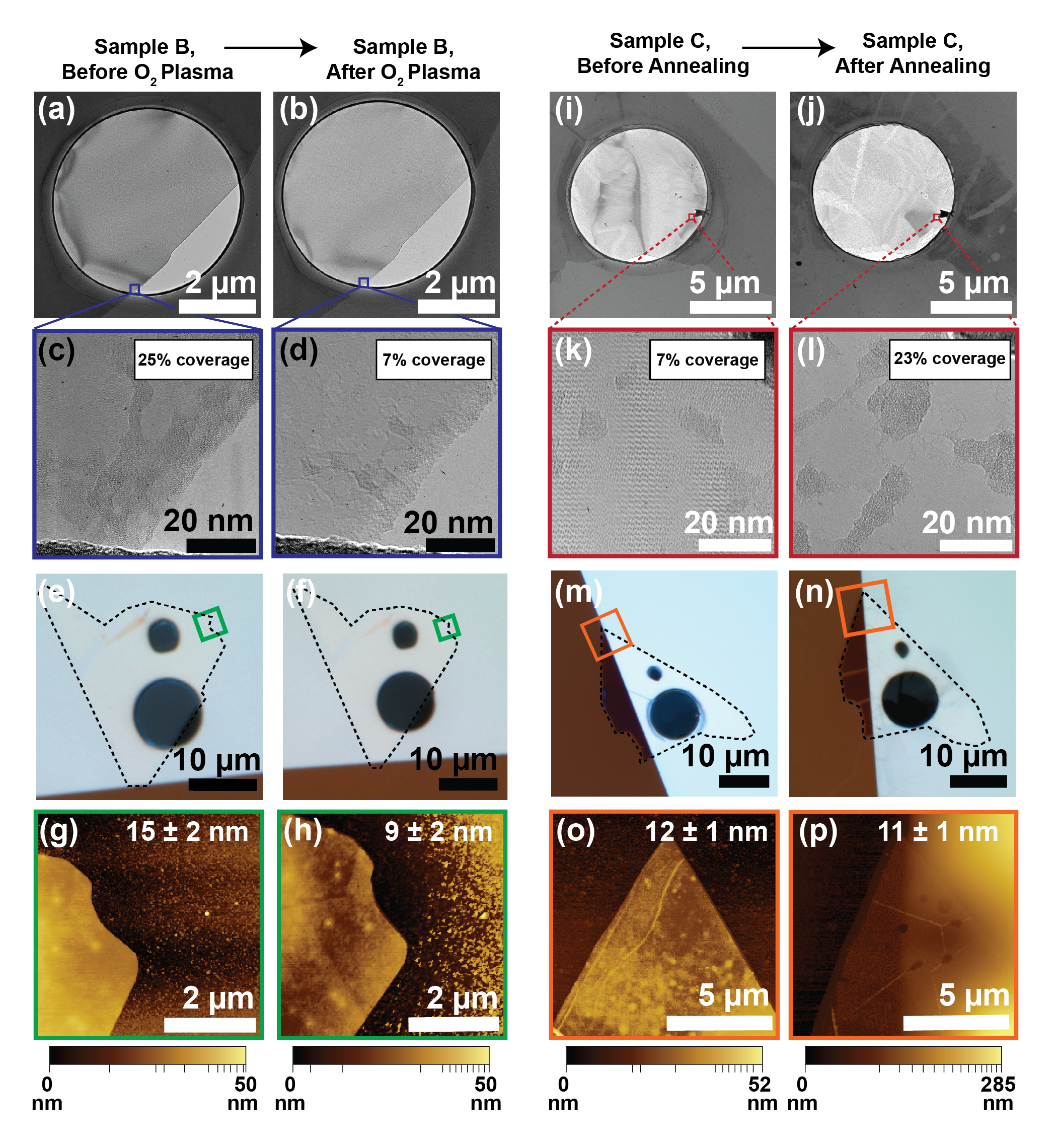
Figure 4 summarizes morphological changes to the exfoliated hBN flakes after oxygen plasma irradiation and annealing. Sample B was irradiated with oxygen plasma for 5 minutes (50 W, 50 sccm O2). TEM images show that on the micron scale, this treatment smoothed wrinkles on the flake (Fig. 4a,b) but had no other obvious effects. On the nanometer scale, however, oxygen plasma irradiation significantly reduced contamination coverage on Sample B from 25% to 7%, with a similar decrease in average contaminant area size (Fig. 4c,d and S4). This treatment also resulted in significant etching of Sample B (15 2 nm 9 2 nm) and a decrease in surface roughness by a factor of approximately 2 (see Tables S2 and S3). This result was unsurprising, given that oxygen plasma treatment is regularly employed as a cleaning method [45, 46, 47].
Sample C was annealed for 2 hours at 850°in an argon environment. TEM images show that annealing resulted in significant cracking and warping of the flake (Fig. 4i,j and S5) and appeared to increase contamination from 7% to 23% in the regions shown in panels (k) and (l). Although, localized, sub-micron holes appeared after treatment, annealing did not result in significant thinning of Sample C (Fig. 4o,p). Annealing also resulted in an increase in roughness by a factor of 2.5 in Sample C (see Table S3). The introduction of cracks and warping, alongside the increase in roughness from annealing is notable. The development such features may be the result of differing rates of expansion and contraction during heating and cooling between the hBN flake and the underlying SiNx membrane [48]. Similarly, the increase in contamination coverage (7% 23%) and average contaminant area (18 nm2 to 56 nm2, see Fig. S5) was unexpected because annealing is also often used as a cleaning technique [49, 50].
III.2 PL Analysis of Treatments
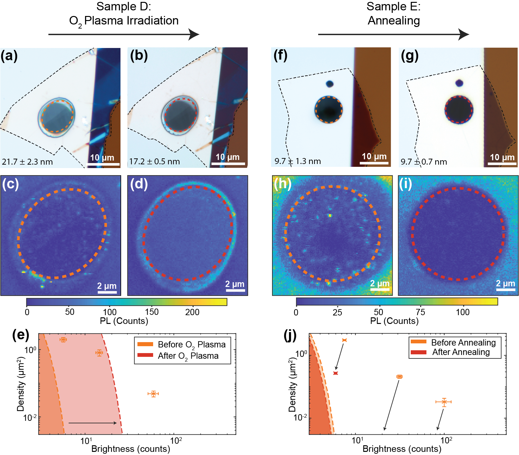
Figure 5 shows how annealing and oxygen plasma treatments affect the optical activity of hBN. Sample D was exposed to oxygen plasma of 50 W at rate of 50 sccm for 5 mins. There are no major changes visible in the hBN flake due to this treatment, but AFM reveals the flake becomes thinner (Fig. 5a,b). The initial PL image shows localized emission over the suspended region, as expected (Fig. 5c). After the oxygen irradiation, the PL signal over the suspended region becomes bright and diffuse without any localized emission visible (Fig. 5d). Figure 5e shows three emitter families before oxygen irradiation. Due to the gradient in brightness across the suspended region, we are not able to perform the analysis on the PL image after the treatment. However, we are able to see that the background level increases significantly after oxygen irradiation.
The brightening and shift to a diffuse morphology observed in Sample D were unexpected since oxygen plasma treatments are typically used as a cleaning procedure [51, 52, 53]. However, these changes could be attributed to damage from etching or oxygen implantation. AFM measurements revealed that the sample is indeed etched (Table S2), and structural changes are also apparent in the TEM image for Sample B (Fig. 4a-d). This damage from oxygen irradiation could increase the background brightness similarly to electron irradiation in the TEM. Although, the effects differ in that oxygen irradiation primarily affects the material’s surface, whereas electron irradiation can impact the bulk [54]. The majority of reports only show oxygen irradiation followed by annealing, as it has been suggested that both treatments are necessary for stable emitter formation [44]. Another possible explanation for the increase in brightness is that oxygen ions are being implanted during the irradiation process. Previous studies have shown that oxygen implantation can alter the optical properties of hBN, including a shift to a diffuse morphology [55].
Sample D exhibited the greatest increase in brightness observed for this experiment, with other samples showing less pronounced changes, thus the treatment does not affect all samples equally. While the majority of samples treated the same way showed an increase in background brightness, there were cases of the background remaining unchanged, including Sample B (Fig. S7a,c). Regardless of a change in brightness, samples consistently exhibited a shift to diffuse emission. When using a lower flow rate for a longer time, a decrease or no change in background was the typical result (Fig. S8). This significant difference highlights the effect’s dependence on treatment recipe, allowing for optimization to achieve the desired outcome.
Sample E was annealed at 850°C for two hours in an Ar environment. After the treatment, the sample maintains its thickness and appears largely unchanged under white light (Fig. 5f,g). On closer inspection, the suspended region shows slight variations in color before annealing and becomes homogeneous afterwards. The emission of the initial PL image (Fig. 5h) displays the same variation pattern as its corresponding white light image (Fig. 5f). After the sample is annealed, few localized emitters remain, and they appear almost uniform with the background (Fig. 5i). Emitter family analysis shows there are three distinct groups before Sample E was annealed and only one after (Fig. 5j). The one emitter group after annealing is dimmer than all of the groups from before the treatment. The background level stays about the same, only decreasing slightly after annealing. This result is in contrast with previous studies, as annealing is regularly used to stabilize and brighten emitters [21, 6]. In this case, emission becomes dimmer without decreasing the background and the localized emission remains unstable, which was consistent across all samples observed in this study. The thinness of the samples may contribute to this outcome, as stable emitters are uncommon at the thicknesses used in this study. It is possible that annealing’s brightening effect only applies to crystals that are suitable to host stable emitters and that samples without improved optical properties are excluded from reports. If PL arises from defects in the lattice, the decrease in intensity could correspond with annealing repairing the lattice. Even though the TEM image of Sample C shows local warping of the sample (Fig. 4i-j), annealing would still be expected to heal the lattice on the global scale. The suspended region of Sample C has no discernible PL signal, confirming the warping does not induce brightening (Fig. S7f). Another explanation for the dimming effect is defect migration and/or transmutation, which potentially reduces emission or blue-shifts the emission wavelength to become undetectable in our experimental setup [28, 56]. Emitter family analysis does not reveal a clear shift in all families following annealing, suggesting significant chemical changes occur during this process. One possible evolution pattern is depicted by the arrows in Figure 5j.
IV Conclusions
In conclusion, we developed a method for sequential, correlated TEM and PL measurements of multi-layer hBN, and we used these complementary techniques, along with AFM and white light imaging, to study the interplay between surface chemistry, contamination, overall morphology, thickness, and optical properties of mechanically exfoliated hBN — all critical considerations in the use of hBN in scalable quantum information and photonics technologies. We show that viscoelastic stamping with PDMS results in considerable residue on the surface of hBN flakes through direct TEM imaging and elemental mapping. We observe that this residue undergoes non-monotonic changes in structure as a result of electron irradiation. We also observe that oxygen plasma treatment results in thinning of hBN and reduces surface residue, but that annealing does not have the same effect. Instead, annealing induces warping and cracking in hBN flakes and results in a re-distribution of surface residue. Furthermore, we show how the optical properties of hBN change as a result of TEM irradiation, oxygen plasma, annealing, and PL measurement itself. In this intermediate thickness regime, all optical emission is subject to photobleaching, and irradiation by TEM or oxygen plasma tends to brighten and diffuse PL emission. The annealing treatment consistently reduces optical activity. These qualitative observations are confirmed by the results of emitter family analysis.
This work sets the stage for further studies on hBN. Such work could include a systematic comparison of different sample preparation methods (i.e. dry transfer, wet transfer, etc.) and the resulting residue or lack thereof; a systematic comparison of the effect of thickness on optical activity (if any); or potentially investigation of strain-induced effects by utilizing more complex substrate geometries. Motivated by the promise of hBN in quantum information and photonics applications, the method introduced in this work may also be adapted to a broad range of 2D materials.
Methods
IV.1 Sample Preparation
TEM grids were purchased from SiMPore with 50-nm-thick SiNx membranes suspended above silicon supports. The suspended SiNx region was 100 100 m large. Holes of varying sizes (1, 5, and 10 m diameter) were drilled in the SiN membranes with a Xe+ ion beam in the Tescan S8252X plasma focused ion beam scanning electron microscope (PFIB-SEM). The PFIB was operated at 15 kV and 300 pA for drilling and the SEM at 5 kV and 100 pA for imaging of SiN memebranes. Once patterned with holes of the desired size and location, we mechanically exfoliated hBN (HQ Graphene) and transferred multi-layer flakes onto the SiN membranes with PDMS stamping. This procedure has been previously reported; see Bhatia et al., 2024 and Keneipp et al., 2024 for more details.
IV.2 Atomic Force Microscopy
AFM measurements were performed using a Bruker Icon AFM. To obtain values for flake thickness and roughness, regions of the flake comparable in thickness (as determined by white-light imaging) to the suspended region were scanned. In general, AFM scans improved when taken areas of the flake supported by the silicon substrate, instead of regions of the flake on the SiNx membrane, as the thin SiNx membrane resulted in a strong, nonuniform background signal in the AFM scans. Additional information about AFM data processing are provided in the Supporting Information.
IV.3 Optical Characterization
PL images were collected using a custom-built confocal microscope with a 592 nm continuous-wave laser (MPB Communications, VF-P-200- 592). The sample was illuminated with circularly polarized light at 100 W unless otherwise noted. A long-pass filter with a cut-on wavelength of 650 nm (Semrock, BLP01- 635R-25) is placed in the collection path to eliminate scattered light. The collected emission goes through a multimode fiber that is either routed to single-photon counting modules (Laser Components, Count T-100) or a spectrometer (Princeton Instruments, Iso-Plane160 and Pixis 100 CCD). For further details, see Patel et al., 2022.
IV.4 Emitter Family Analysis
Analysis used to categorize emitter groups is based on previous work by Breitweiser et al., 2020. In this paper, we plot a histogram of the intensity of each pixel in the selected region (as indicated by dashed ovals in Figures 3 and 5). Fits of the histogram determine the background level and each emitter group. We extract density and brightness parameters from the emitter groups. We select the number of distributions used based on the reduced chi squared value of the overall fit.
IV.5 TEM Characterization
TEM characterization was performed in the JEOL JEM-F200 S/TEM equipped with a Gatan OneView Camera and JEOL dual SDD detectors for EDS spectra acquisition. The JEOL F200 was operated at 80kV in both TEM mode and STEM mode. All TEM data were processed using Gatan DigitalMicrograph and ImageJ.
IV.6 Sample Treatments
Oxygen plasma irradiation treatment was performed on hBN samples in an Anatech SCE 108 Barrel Asher. TEM grids with hBN flakes were secured to a 4-inch, 500 m Si and 1500 Å silicon oxide wafer using kapton tape. This wafer was placed into the process chamber with oxygen plasma at 50W with flow rate of 25 or 50 sccm for 5 or 10 minutes, respectively.
Annealing treatment was performed on hBN samples in the Carbolite HZS 1200°C 3 Zone Split Tube Furnace. The tube used is dedicated to hBN use only and cleaned prior to treatment with isopropyl alcohol and pressurized nitrogen gas. Samples are placed in an alumina ceramic boat and annealed in an Ar environment at 850°C for two hours.
V Acknowledgements
J.A.G. and L.C.B. acknowledge support from the NSF under awards DMR-1922278 and DMR-2019444. J.A.G. also acknowledges support from an NSF Graduate Research Fellowship (DGE-1845298). P.B., R.N.K., T.T.S., B.N.S., A.S.U., and M.D. acknowledge support from DOE grant DE-SC0023224 on advanced in-situ TEM analysis and ex-situ studies of 2D hBN. P.B. was also funded by NIH grant R01HG012413 for the development of hBN/graphene nanopores. This work was carried out in part at the Singh Center for Nanotechnology, which is supported by the NSF National Nanotechnology Coordinated Infrastructure Program under grant NNCI-2025608. The authors also acknowledge use of facilities and instrumentation supported by NSF through the University of Pennsylvania Materials Research Science and Engineering Center (MRSEC) (DMR-1720530). Finally, the authors also wish to thank Dr. Douglas Yates and Dr. Jamie Ford for their assistance with TEM characterization and FIB milling of substrates.
References
- Shaik and Palla [2021] A. B. D.-a.-j.-w.-i. Shaik and P. Palla, Scientific Reports 11, 1 (2021).
- Jungwirth et al. [2016] N. R. Jungwirth, B. Calderon, Y. Ji, M. G. Spencer, M. E. Flatté, and G. D. Fuchs, Nano Letters 16, 6052 (2016).
- Dean et al. [2010] C. R. Dean, A. F. Young, I. Meric, C. Lee, L. Wang, S. Sorgenfrei, K. Watanabe, T. Taniguchi, P. Kim, K. L. Shepard, and J. Hone, Nature Nanotechnology 5, 722 (2010).
- Yu et al. [2013] G. L. Yu, R. Jalil, B. Belle, A. S. Mayorov, P. Blake, F. Schedin, S. V. Morozov, L. A. Ponomarenko, F. Chiappini, S. Wiedmann, U. Zeitler, M. I. Katsnelson, A. K. Geim, K. S. Novoselov, and D. C. Elias, Proceedings of the National Academy of Sciences of the United States of America 110, 3282 (2013).
- Kuiri et al. [2015] M. Kuiri, C. Kumar, B. Chakraborty, S. N. Gupta, M. H. Naik, M. Jain, A. K. Sood, and A. Das, Nanotechnology 26, 10.1088/0957-4484/26/48/485704 (2015).
- Tran et al. [2016a] T. T. Tran, C. Elbadawi, D. Totonjian, C. J. Lobo, G. Grosso, H. Moon, D. R. Englund, M. J. Ford, I. Aharonovich, and M. Toth, ACS Nano 10, 7331 (2016a).
- Exarhos et al. [2017] A. L. Exarhos, D. A. Hopper, R. R. Grote, A. Alkauskas, and L. C. Bassett, ACS Nano 11, 3328 (2017).
- Mendelson et al. [2019] N. Mendelson, Z. Q. Xu, T. T. Tran, M. Kianinia, J. Scott, C. Bradac, I. Aharonovich, and M. Toth, ACS Nano 13, 3132 (2019).
- Patel et al. [2022] R. N. Patel, D. A. Hopper, J. A. Gusdorff, M. E. Turiansky, T.-Y. Huang, R. E. K. Fishman, B. Porat, C. G. Van de Walle, and L. C. Bassett, PRX Quantum 3, 1 (2022).
- Exarhos et al. [2019] A. L. Exarhos, D. A. Hopper, R. N. Patel, M. W. Doherty, and L. C. Bassett, Nature Communications 10, 10.1038/s41467-018-08185-8 (2019).
- Chejanovsky et al. [2021] N. Chejanovsky, A. Mukherjee, J. Geng, Y. C. Chen, Y. Kim, A. Denisenko, A. Finkler, T. Taniguchi, K. Watanabe, D. B. R. Dasari, P. Auburger, A. Gali, J. H. Smet, and J. Wrachtrup, Nature Materials 20, 1079 (2021).
- Guo et al. [2023] N. J. Guo, S. Li, W. Liu, Y. Z. Yang, X. D. Zeng, S. Yu, Y. Meng, Z. P. Li, Z. A. Wang, L. K. Xie, R. C. Ge, J. F. Wang, Q. Li, J. S. Xu, Y. T. Wang, J. S. Tang, A. Gali, C. F. Li, and G. C. Guo, Nature Communications 14, 10.1038/s41467-023-38672-6 (2023).
- Patel et al. [2024] R. N. Patel, R. E. Fishman, T. Y. Huang, J. A. Gusdorff, D. A. Fehr, D. A. Hopper, S. A. Breitweiser, B. Porat, M. E. Flatté, and L. C. Bassett, Nano Letters 10.1021/acs.nanolett.4c01333 (2024).
- Stern et al. [2024] H. L. Stern, C. M. Gilardoni, Q. Gu, S. Eizagirre Barker, O. F. Powell, X. Deng, S. A. Fraser, L. Follet, C. Li, A. J. Ramsay, H. H. Tan, I. Aharonovich, and M. Atatüre, Nature Materials 23, 1379 (2024).
- Akbari et al. [2021] H. Akbari, W. H. Lin, B. Vest, P. K. Jha, and H. A. Atwater, Physical Review Applied 15, 1 (2021).
- Proscia et al. [2018] N. V. Proscia, Z. Shotan, H. Jayakumar, P. Reddy, C. Cohen, M. Dollar, A. Alkauskas, M. Doherty, C. A. Meriles, and V. M. Menon, Optica 5, 1128 (2018).
- Sajid and Thygesen [2020] A. Sajid and K. S. Thygesen, 2D Materials (2020).
- Yang et al. [2022] F. Yang, G. Stando, A. Thompson, D. Gundurao, L. Li, and H. Liu, Accounts of Materials Research 3, 1022 (2022).
- Li et al. [2023] S. X. Li, T. Ichihara, H. Park, G. He, D. Kozawa, Y. Wen, V. B. Koman, Y. Zeng, M. Kuehne, Z. Yuan, S. Faucher, J. H. Warner, and M. S. Strano, Communications Materials 4, 1 (2023).
- Wigger et al. [2019] D. Wigger, R. Schmidt, O. Del Pozo-Zamudio, J. A. Preuß, P. Tonndorf, R. Schneider, P. Steeger, J. Kern, Y. Khodaei, J. Sperling, S. M. De Vasconcellos, R. Bratschitsch, and T. Kuhn, 2D Materials 6, 10.1088/2053-1583/ab1188 (2019).
- Breitweiser et al. [2020] S. A. Breitweiser, A. L. Exarhos, R. N. Patel, J. Saouaf, B. Porat, D. A. Hopper, and L. C. Bassett, ACS Photonics 7, 288 (2020).
- Fournier et al. [2021] C. Fournier, A. Plaud, S. Roux, A. Pierret, M. Rosticher, K. Watanabe, T. Taniguchi, S. Buil, X. Quélin, J. Barjon, J. P. Hermier, and A. Delteil, Nature Communications 12, 1 (2021).
- Hayee et al. [2020] F. Hayee, L. Yu, J. L. Zhang, C. J. Ciccarino, M. Nguyen, A. F. Marshall, I. Aharonovich, J. Vučković, P. Narang, T. F. Heinz, and J. A. Dionne, Nature Materials 19, 534 (2020).
- Alem et al. [2009] N. Alem, R. Erni, C. Kisielowski, M. D. Rossell, W. Gannett, and A. Zettl, Physical Review B 80, 155425 (2009).
- Bui et al. [2023] T. A. Bui, G. T. Leuthner, J. Madsen, M. R. A. Monazam, A. I. Chirita, A. Postl, C. Mangler, J. Kotakoski, and T. Susi, Small 19, 10.1002/smll.202301926 (2023).
- Keneipp et al. [2024] R. N. Keneipp, J. A. Gusdorff, P. Bhatia, T. T. Shin, L. C. Bassett, and M. Drndić, Journal of Physical Chemistry C 128, 8741 (2024).
- Li et al. [2019] C. Li, Z.-Q. Xu, N. Mendelson, M. Kianinia, M. Toth, and I. Aharonovich, Nanophotonics 8, 2049 (2019).
- Venturi et al. [2024] G. Venturi, S. Chiodini, N. Melchioni, E. Janzen, J. H. Edgar, C. Ronning, and A. Ambrosio, Laser and Photonics Reviews 18, 39 (2024).
- Mohajerani et al. [2024] S. S. Mohajerani, S. Chen, A. Alaei, T. Chou, N. Liu, Y. Ma, L. Xiao, S. S. Lee, E.-H. Yang, and S. Strauf, ACS Photonics 11, 2359 (2024).
- Chen et al. [2023] Y. Chen, A. Gale, K. Yamamura, J. Horder, A. Condos, K. Watanabe, T. Taniguchi, M. Toth, and I. Aharonovich, Applied Physics Letters 123, 10.1063/5.0155311 (2023).
- Tran et al. [2016b] T. T. Tran, K. Bray, M. J. Ford, M. Toth, and I. Aharonovich, Nature Nanotechnology 11, 37 (2016b).
- Ngoc et al. [2018] H. Ngoc, M. Duong, M. Anh, P. Nguyen, M. Kianinia, T. Ohshima, H. Abe, K. Watanabe, T. Taniguchi, J. H. Edgar, I. Aharonovich, and M. Toth, ACS Applied Materials and Interfaces 10.1021/acsami.8b07506 (2018).
- Egerton et al. [2004] R. Egerton, P. Li, and M. Malac, Micron 35, 399 (2004).
- Rykaczewski et al. [2007] K. Rykaczewski, W. B. White, and A. G. Fedorov, Journal of Applied Physics 101, 10.1063/1.2437065 (2007).
- Egerton [2019] R. Egerton, Micron 119, 72 (2019).
- Bhatia et al. [2024] P. Bhatia, T. T. Shin, K. Kavetsky, B. N. Sailors, G. Siokos, A. S. Uy-Tioco, R. N. Keneipp, J. A. Gusdorff, L. C. Bassett, and M. Drndić, Micron , 103747 (2024).
- Cheliotis and Zergioti [2024] I. Cheliotis and I. Zergioti, 2D Materials 11, 022004 (2024).
- Jain et al. [2018] A. Jain, P. Bharadwaj, S. Heeg, M. Parzefall, T. Taniguchi, K. Watanabe, and L. Novotny, Nanotechnology 29, 265203 (2018).
- Jang et al. [2023] D. J. Jang, M. M. Haidari, J. H. Kim, J.-Y. Ko, Y. Yi, and J. S. Choi, Nanomaterials 13, 1494 (2023).
- Kotakoski et al. [2010] J. Kotakoski, C. H. Jin, O. Lehtinen, K. Suenaga, and A. V. Krasheninnikov, Physical Review B 82, 113404 (2010).
- Dai et al. [2023] C. Dai, D. Popple, C. Su, J.-H. Park, K. Watanabe, T. Taniguchi, J. Kong, and A. Zettl, Communications Chemistry 6, 108 (2023).
- Gilbert et al. [2017] S. M. Gilbert, G. Dunn, A. Azizi, T. Pham, B. Shevitski, E. Dimitrov, S. Liu, S. Aloni, and A. Zettl, Scientific Reports 7, 15096 (2017).
- Neumann et al. [2023] M. Neumann, X. Wei, L. Morales-Inostroza, S. Song, S. G. Lee, K. Watanabe, T. Taniguchi, S. Götzinger, and Y. H. Lee, ACS Nano 17, 11679 (2023).
- Fischer et al. [2021] M. Fischer, J. M. Caridad, A. Sajid, S. Ghaderzadeh, M. Ghorbani-Asl, L. Gammelgaard, P. Bøggild, K. S. Thygesen, A. V. Krasheninnikov, S. Xiao, M. Wubs, and N. Stenger, Science advances 7, 10.1126/sciadv.abe7138 (2021).
- Na et al. [2021] Y. S. Na, J. H. Kim, S. Kang, J. H. Jeong, S. Park, D. H. Kim, K. Ihm, K. Watanabe, T. Taniguchi, Y.-K. Kwon, Y. D. Kim, and G.-H. Lee, 2D Materials 8, 045041 (2021).
- Jadwiszczak et al. [2021] J. Jadwiszczak, D. J. Kelly, J. Guo, Y. Zhou, and H. Zhang, ACS Applied Electronic Materials 3, 1505 (2021).
- Kim et al. [2016] S. Kim, M. S. Choi, D. Qu, C. H. Ra, X. Liu, M. Kim, Y. J. Song, and W. J. Yoo, 2D Materials 3, 035002 (2016).
- Zhang et al. [2023] G. Zhang, Y. Chang, and B. Yan, Crystals 13, 304 (2023).
- Garcia et al. [2012] A. G. F. Garcia, M. Neumann, F. Amet, J. R. Williams, K. Watanabe, T. Taniguchi, and D. Goldhaber-Gordon, Nano Letters 12, 4449 (2012).
- Lin et al. [2012] Y.-C. Lin, C.-C. Lu, C.-H. Yeh, C. Jin, K. Suenaga, and P.-W. Chiu, Nano Letters 12, 414 (2012).
- Griffiths and Walther [2010] A. J. V. Griffiths and T. Walther, Journal of Physics: Conference Series 241, 012017 (2010).
- Hugenschmidt et al. [2022] M. Hugenschmidt, K. Adrion, A. Marx, E. Müller, and D. Gerthsen, Microscopy and Microanalysis 2, 10.1093/micmic/ozac003 (2022).
- Mitchell and Mitchell [2015] D. R. G. Mitchell and D. R. G. Mitchell, Australian Institute for Innovative Materials - Papers 73, 36 (2015).
- Vogl et al. [2019] T. Vogl, M. W. Doherty, B. C. Buchler, Y. Lu, and P. K. Lam, Nanoscale 11, 14362 (2019).
- Mendelson et al. [2021] N. Mendelson, D. Chugh, J. R. Reimers, T. S. Cheng, A. Gottscholl, H. Long, C. J. Mellor, A. Zettl, V. Dyakonov, P. H. Beton, S. V. Novikov, C. Jagadish, H. H. Tan, M. J. Ford, M. Toth, C. Bradac, and I. Aharonovich, Nature Materials 20, 321 (2021).
- Weston et al. [2018] L. Weston, D. Wickramaratne, M. Mackoit, A. Alkauskas, and C. G. Van De Walle, Physical Review B 97, 10.1103/PhysRevB.97.214104 (2018).