Rectification from band gap oscillation
Abstract
We consider a chain of divalent atoms with two electronic orbitals per atom, whose length is periodically oscillating with time in response to an external oscillating pressure source. We introduce both inter-orbital and intra-orbital hopping between neighboring atoms which as a consequence of the oscillating lattice separation, are also periodically oscillating in time. Within the tight binding approximation and in the limit of very small inter-orbital hopping, we get two bands separated by an indirect band gap which itself oscillates due to the oscillating chain length. Under suitable choice of hopping parameters (about which it oscillates) and orbital energies, we show that there can be a periodic metal-insulator transition in the half-filled system. If the frequency of the metal-insulator transition resonates with an externally applied alternating electric field, it can give rise to the phenomena of half-wave rectification wherein in one half of the cycle the system is metallic and conducting, where as in the other half of the cycle it is insulating and non-conducting.
I Introduction
Metal-insulator transitions [1] in different systems have been studied extensively in the community for the last few decades. A metal-insulator transition can be induced by thermal fluctuations i.e., by varying temperature [2], by doping [3], by varying pressure [4, 5, 6, 7, 8], by tuning magnetic field [9, 10], by tuning disorder [11], by structural deformations [12] and by quantum fluctuations at temperature [13]. Out of all these possible routes, applying pressure to induce a metal-insulator transition has a simple physics behind it. Within the paradigm of band theory where due to the quasiparticle picture of effective degrees of freedom one can ignore the electron electron correlation effects, compressing the system decreases the lattice spacing and hence increases the overlap, or equivalently the hopping between the atomic orbitals and the bandwidth of the bands. This can make a band insulator at , a band metal in suitable systems. However, there are wide range of systems where electron electron correlation is strong and can not be neglected. For example [14, 15] in the undoped state is a Mott insulator [16, 17] which can undergo pressure induced transition to a metallic state [18]. This happens because compressive pressure can effectively reduce the electron electron correlation to hopping amplitude ratio and make the system metallic. Pressure has also been found to induce superconductivity in some systems [19].
In this paper, we are interested specifically in the pressure dependence of metal-insulator transition. We consider a half-filled monoatomic chain consisting of two orbitals per atom having length which is being periodically stretched and compressed using an external oscillating pressurizer. This implies that the lattice separation is also a periodically oscillating function of time and hence the hopping amplitude also carries out an out of phase oscillation as compared to the lattice separation. If oscillates about the metal-insulator transition point, then it enters the metallic and band insulator phases periodically. This means this system behaves as a two-level resistor with resistivity values and in periodic cycles of the metal-insulator transition frequency . This has significant technological implications which will be detailed in the next paragraph.
The periodic metal-insulator transitions can potentially be used for voltage rectification purposes. We know that electrical transformers [20] use rectification properties of junction diodes [20] for converting alternating currents to direct currents which is required for running our electrical appliances. A junction is made from a -type semiconductor which is basically hole doped and an -type semiconductor which is electron doped. At their junction a depletion region is formed which decreases in width when the device is forward biased as opposed to the increasing width when the device is reverse biased. Ideally, therefore the device has very low resistance when forward biased and very high resistance when reverse biased and hence a single diode acts as a half-wave rectifier to an alternating voltage. We propose that a system periodically stretched and compressed with frequency can serve as a half-wave rectifier for an alternating voltage with same frequency . In the metallic phase cycle, the system conducts while in the band insulator cycle the system does not conduct any electricity. Therefore, junction diodes in transformers can be replaced by such systems which can harbor a periodic metal-insulator transition in response to periodic pressure.
II Model
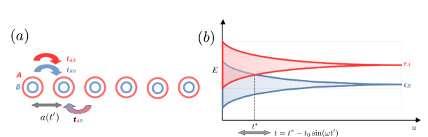
We consider a one dimensional atomic chain made up of atoms each having two atomic orbitals with energies and . The chain is being periodically stretched and compressed with a frequency such that the length of the chain as a function of time is , where . This means the inter-atomic lattice spacing also has the same periodic dependence , where . We will consider periodic boundary condition here, so that the system is actually a ring with equispaced atoms which is being radially stretched and compressed. Hence the first Brillouin zone () will also oscillate periodically with time with the spacing between discrete crystal momentum values being . Therefore, when the length is stretched the values come closer while the also shrinks. On the other hand when the length is compressed the values move farther while the also expands.
We consider both intra and inter orbital hopping between neighboring atoms, the hopping amplitudes of which we call and respectively. As the hopping amplitude is inversely proportional to the inter atomic spacing, its time dependence goes like () as compared to which goes like . Within the tight binding approximation, the electron is tightly bound to the nuclei and we introduce a weak hopping between the neighboring atoms, which is time dependent here. Therefore, we take the following linear combination of orthonormal atomic orbitals as our ansatz solution of the wavefunction of the Hamiltonian,
| (1) |
Putting this in the Schrdinger equation and taking inner product with and we get,
| (2) | |||
| (3) |
| (4) |
Solving the characteristic equation gives us the dispersion relations for the two bands which are,
| (5) |
where and . While inter-orbital hopping tries to open a direct band gap between the two bands i.e., the lower band maxima and upper band minima occur at the same point, the intra-orbital hoppings favour an indirect band gap where there is a difference in the crystal momentum of the lower band maxima and upper band minima. It is an interesting observation that tuning the strengths of and out of phase with time can give rise to oscillatory metal-insulator transitions at half-filling for suitable choice of their values at . However, we would not elaborate on this since it seems physically unrealistic to have out of phase oscillations of hopping parameters in a system which is being periodically stretched and compressed. Physically, all the hopping parameters should oscillate in phase. Therefore, we would fix the value of at to a low value or to zero and study the periodic metal-insulator transition due to periodically oscillating intra-orbital hopping . How this happens will be elaborated in the following paragraph. It is to be noted that the sole purpose of retaining the term is because in an experimental sample we will in principle have this term present.
Fig 1 shows the tight binding chain with two orbitals per atom with orbital energies and such that . We also consider intra-orbital hoppings . Let us first understand the static case. In the limit of vanishing , we basically get two decoupled bands whose bandwidth is an decreasing function of lattice separation and increasing function of hopping amplitude as shown in Fig 1. There is a point corresponding to which marks the onset of metallic behavior for a half-filled system from insulating behavior (at temperatures where thermal fluctuations are not able to provide the minimum single particle excitation energy) as we decrease lattice separation. This is an example of metal insulator transition. Now if we stretch and compress our system about periodically such that there is an out of phase oscillation in about , we pass through the metal-insulator transition periodically i.e., in one half of the cycle the system is an insulator where as in the other half of the cycle the system is a metal. In the band insulator phase, the lower band is completely filled which means there are electrons in the system and at or low temperatures, a small electric field can not provide the minimum energy excitation and hence can not conduct electricity. When the same system undergoes a transition to the metallic phase, the bands overlap and we have partially filled bands which would respond to a small electric field by conducting current at half-filling. In the following section, we will see how we use this physics for rectification of alternating electric fields.
III Rectification
We all know that a semiconductor device consisting of a junction of a type and an type doped semiconductor, also known as a diode has very small resistance when it is forward biased and very high resistance when it is reverse biased. A type semiconductor like silicon doped with boron is the one where the majority charge carriers are holes where as type semiconductor like silicon doped with phosphorous is the one where the majority charge carriers are electrons. The depletion region barrier at the junction of two types of semiconductors is reduced when the system is forward biased enabling a flow of current where as when reverse biased the barrier height increases and hinders current flow. So it acts like a switch enabling current flow in one direction and inhibiting current flow if polarity is reversed. Thus, if we apply an alternating electric field across its terminal, the junction diode will enable current flow in phase with the voltage during one cycle where as in the other half of the cycle it will give no current response. This is known as half-wave rectification.
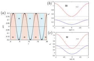
We propose a novel mechanism of half-wave rectification through periodic metal-insulator transition in a chain of atoms, the length of which is being stretched and compressed periodically. In the previous section we have shown that if the intra-orbital hopping parameters oscillate about as shown in Fig 1 and the system is half-filled, then the system periodically enters a metallic phase and a band insulator phase. To characterize these two phases we define the band gap which is equal to for in our model. For the band insulator phase, i.e., the valence band maxima lies below the conduction band minima. Where as for the metallic phase, when the bands overlap and the conduction band minima lies below the valence band maxima. Fig 2 shows the plot of as function of the time for the hopping parameters ( has been taken to be zero) and onsite orbital energies . These parameters correspond to when the valence band maximum at just equals to the conduction band minimum at . The time period of this oscillation is where . At half-filling, in the red shaded regions the system is a band insulator (BI) where as in the blue shaded regions the system is metal (M). Fig 2 shows the band dispersions at and where the system is a band insulator and a metal respectively at half-filling.
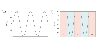
Now if we consider an alternating electric field or equivalently a voltage which has the same time period as the periodic pressure on the chain then the half-filled chain would conduct in the half-cycle where it is a metal and will not conduct in the other half-cycle. This is shown in Fig 3. So, just like a p-n junction diode it acts like a half-wave rectifier, only the principles of operation are very different.
IV Conclusion
In conclusion, we have proposed a one dimensional model of atoms in a chain whose length is being stretched and compressed periodically for example by providing oscillating pressure. As a consequence we see, that it is possible for the system to undergo repeated metal insulator transitions which can be used for the purpose of half-wave rectification of alternating voltages. Therefore it can potentially replace junction diodes whose rectification properties are used in transformers to convert alternating current to direct current. Moreover, our theory can be extended to systems where electron-electron interaction effects can not be neglected, for example in Mott insulators. Stretching reduces hopping and the electron -electron interaction and hopping ratio, becomes large and the system behaves like a Mott insulator at half-filling. While if become large i.e., if we compress the system, it will behave like a metal at half-filling. So, in systems where quasiparticle picture holds good and band theory works as well as in systems where electron-electron interaction plays a crucial role, periodic stretching and compression can be potentially used for rectification purposes, as in transformers replacing the widespread use of junction diodes.
References
- [1] Masatoshi Imada, Atsushi Fujimori, and Yoshinori Tokura Rev. Mod. Phys. 70, 1039 (1998).
- [2] F. J. Morin Phys. Rev. Lett. 3, 34 (1959).
- [3] N. F. Mott, Advances in Physics, 21(94), 785–823 (1972).
- [4] Yang, Y., Yu, F., Wen, X. et al., Nat Commun 14, 2260 (2023).
- [5] Bikash Padhi, Philip W. Phillips, Phys. Rev. B 99, 205141 (2019).
- [6] Andreas Giesekus and L. M. Falicov, Phys. Rev. B 44, 10449 (1991).
- [7] Victor Pardo and Warren E. Pickett, Phys. Rev. B 85, 045111 (2012).
- [8] P. Homm et al.,APL Mater. 9, 021116 (2021).
- [9] T. Wang et.al., Phys. Rev. Lett. 72, 709 (1994).
- [10] E. V. Gorbar et. al., Phys. Rev. B 66, 045108 (2002).
- [11] P. W. Anderson, Phys. Rev. 109, 1492 (1958).
- [12] C. H. Lee et. al., J. Phys.: Condens. Matter 13 L45 (2001).
- [13] Matthias Vojta, Rep. Prog. Phys. 66 2069–2110 (2003).
- [14] D. B. McWhan and J. P. Remeika, Phys. Rev. B 2, 3734 (1970).
- [15] D. B. McWhan et.al., Phys. Rev. B 7, 1920 (1973).
- [16] N. F. Mott Philosophical Magazine, 19, 160, 835-852 (1969).
- [17] N. F. Mott, Contemporary Physics, 14, 5, 401-413 (1973).
- [18] D. B. McWhan and T. M. Rice, Phys. Rev. Lett. 22, 887 (1969).
- [19] Milton S. Torikachvili et .al., Phys. Rev. Lett. 101, 057006 (2008).
- [20] Electronic devices and circuit theory, Robert L. Boylestad, Louis Nashelsky, Pearson Education, USA (2013).