Exact theory of edge diffraction and launching of transverse electric plasmons at two-dimensional junctions
Abstract
An exact solution for electromagnetic wave diffraction at the junction of two-dimensional electron systems (2DES) is obtained and analyzed for electric field polarized along the edge. A special emphasis is paid to the metal-contacted and terminated edges. In the former case, electric field at the edge tends to zero; in the latter case, it tends to a finite value which is screened by 2d system in an anomalous fashion. For both types of edge and capacitive type of 2d conductivity, an incident wave excites transverse electric 2d plasmons. The amplitude of excited TE plasmons is maximized and becomes order of incident wave amplitude for capacitive impedance of 2DES order of free space impedance. For both large and small 2DES impedance, the amplitude of TE plasmons tends to zero according to the power laws which are explicitly derived.
Junctions of two-dimensional electron systems (2DES) their contacts with metals are among the central objects in the 2D optoelectronics. Such junctions are capable to generate photocurrent [1, 2, 3, 4], which ensures their rich applications both in practical optoelectronics and fundamental studies of light-matter interactions. While numerous studies were devoted to the microscopic theories of electronic transport at the junctions in external electromagnetic (EM) fields [5, 6, 7, 8], much less is known about diffraction of the EM fields at these junctions. The problem of EM wave diffraction at the laterally non-uniform 2DES is complex and is typically studied with electromagnetic simulations [9, 10] or approximate plane wave representations of the local fields [11, 12]. Quite recently, it was realized that a powerful analytical method for solving integral scattering-type equations in the semi-infinite domains, the Wiener-Hopf method, can be successfully applied to the edge diffraction in 2DES [13, 14, 15, 16, 17]. Several remarkable analytical results have been obtained using this technique. These include a universal value of electromagnetic absorbance at the metal-2DES contact [16], a universal value of 2D plasmons’ amplitude launched at the terminated 2D edge [14], but are not limited to the latter.
All previous studies of the edge diffraction in 2DES [13, 16, 14] dealt with incident fields having the magnetic vector along the edge of 2DES. Consequently, the electric field was orthogonal to edge. For such a polarization, the local electric field was greatly enhanced via the dynamic lightning-rod effect. Such enhancement has been confirmed experimentally via studies of polarization-dependent photocurrent at metal-graphene junctions [18, 19, 20].
Another polarization of the incident field, where the electric vector is directed along the edge, did not yet gain attention in the theory of 2D edge diffraction. The present paper fills in this gap. For such polarization, electric field is expected to be suppressed, especially if a 2DES is contacting a metal with very large conductivity. While field suppression is not as appealing as field enhancement, its particular magnitude is important for design of polarization-sensitive and polarization-resolving photodetectors [19, 21]. Another intriguing aspect of such polarization is the possibility to excite the two-dimensional transverse electric (TE) plasmons [22] in such a simple scattering geometry. Such waves can exist only for capacitive type of 2DES conductivity , if the notation for time-dependent fields is assumed. While the conductivity of free-carrier interband motion is always inductive, the capacitive conductivity can be expected near the interband absorption edges [23]. Particularly, this can occur for photon energies close to the band gap (if present) [23] or close to the twice the Fermi energy, , in the case of doped graphene [22, 24].
We proceed to obtain an analytical solution for EM wave diffraction at the junction between 2D electron systems in TE polarization, i.e. for electric vector of the wave directed along the edge. Our particular emphasis will be on the asymptotic values of the field near the junction and away from it, as well on the amplitude of edge-launched TE plasmons.
The setting under study is shown in Fig. 1 (a). 2D electron systems with conductivities and lie in the plane and are contacting along a straight line . Electric field of the incident wave is directed along the -axis and has the form , here is the -component of the wave vector, is the wave number, and is the gliding angle. The harmonic time dependence of all quantities will be assumed and hitherto skipped, so will be skipped the subscript for -component. The scattering equation for electric field in the 2DES plane has the form
| (1) |
where is the free-space impedance ( in Gaussian units or Ohm in SI units); , the Hankel function of the zeroth order, is the fundamental solution of the wave equation in two dimensions, and is the distribution of wave-induced surface currents in 2DES. To form a complete scattering equation with one unknown function, the electric field , we use the Ohm’s law in the local form , where the conductivity varies in a stepwise fashion .
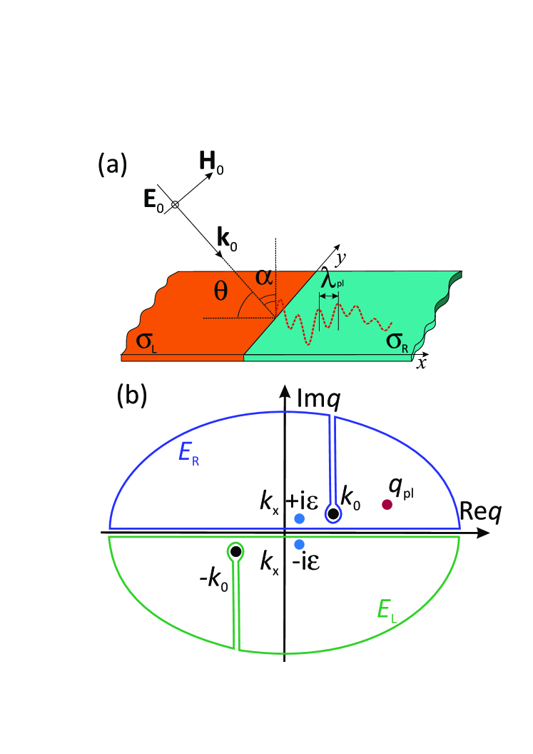
Solution of (1) relies on the Wiener-Hopf technique. It involves the splitting of the total field into the left and right components, , Fourier transform of the governing equation with passing to the wave vector -variable, and studies of the emerging functions of complex -variable. Before Fourier transforming, it is reasonable to ’bound’ all functions to a finite region of the real space. We replace the source field according to , which mimics constraining the incident beam by the aperture of size . We also assume some residual dissipation in the materials surrounding the 2DES, which amounts to the replacement , , in the argument of the electromagnetic propagator. We shall see that the final results will not depend on auxiliary values of and . Still, retaining their finite magnitude is important in the course of solution.
The Fourier transformed scattering equation (1) has the form
| (2) |
where the transverse-electric screening functions are
| (3) |
The key role in the subsequent solution will be played by the ’factorized functions’ and . They are analytic in the upper and lower half-planes of the complex -variable. The factorization here will be achieved with the Cauchy theorem applied to a narrow strip enclosing the real axis, though semi-analytical approaches are also available [16, 25]. The result of Cauchy factorization reads as
| (4) |
After algebraic rearrangements, Eq. (2) takes the form
| (5) |
where the first terms of lhs and rhs are analytic in the upper half-plane, and the second terms of lhs and rhs are analytic in the lower half-plane. Therefore, one can equate the function analytic in the respective half-planes term-by-term. This results in the final solution for electric fields
| (6) | |||
| (7) |
Equations (6) solve the scattering problem in the Fourier domain.
We shall limit our discussion to the terminated () and metal-contacted () edges. The resulting quantities will be equipped with symbols (termination) and (contact). The subscript of the ’right’ material functions will be skipped, , . After taking the proper limit of the ’left’ dielectric function, we arrive at the explicit form of ’right’ electric field for both types of the edge:
| (8) | |||
| (9) |
The behavior of electric field in the immediate vicinity of the junction, , can be understood by analyzing the decay of Fourier components at large . The spectrum of metal-contacted field (9) rapidly decays as , which implies that the field at the junction is zero. This is quite expected, as the electric field in metal is absent, while its tangential component is continuous across the interface. The electric field spectrum for terminated junction (8) decays . It implies that the junction field is finite. Its value can be linked to the residue at infinity
| (10) |
A fully analytical result can be obtained for normal incidence, . In that case, the principal value part of Cauchy integral (4) is zero by the virtue of integrand anti-symmetry. The pole part of the Cauchy integral is evaluated trivially, which results in . Noteworthy is the resulting ’anomalous’ screening of the incident field:
| (11) |
It contrasts to the linear screening of the incident field by an extended 2D electron system, . Queerly speaking, truncating a half of 2D system results in halving of the power in the screening law.
It is instructive to reveal the singularities of the field spectra . They are linked to the waves emitted upon the diffraction. Figure 2 (a) shows the spectra of electric field for metal-contacted 2DES with different values of surface conductivity. The external wave is incident with . Naturally, all spectral curves have a pole at that corresponds to the incident field screened by the 2DES. Another (weaker) singularity is present at in the absence of 2DES (, black line). The spectrum of electric field behaves as . This corresponds to the radiation of a ’line of dipoles’ arranged along the contact line. In real space, such a weak singularity corresponds to the cylindrical wave . With enhancement in 2DES conductivity, this ’dipole radiation’ is largely modified. For inductive 2d conductivity, , the singularity is smeared, and all its traces fade at . We can speculate that inductance of 2d electrons prevents the propagation of dipole radiation.
For capacitive 2d conductivity, , the spectral features are more interesting. An initial weak singularity at shifts rightwards and becomes a well-developed pole. The width of spectral peak remains finite only by the virtue of dissipative conductivity, . The situation corresponds to the launching of transverse electric two-dimensional plasmons by the edge. Figure 2 (b) illustrates this situation in real space: a slow modulation of electric field with period is threaded with faster modulation due to the plasma wave. The plasmon wavelength shrinks with increasing .
A more detailed study of the real-space electric field can be achieved by inverse Fourier transforming Eq. (6):
| (12) |
We close the integration contour for in the upper half plane, blue line in Fig. 1 (b), and apply the residue theorem. The first residue is evaluated at and produces the incident wave screened by the 2DES. Another residue is evaluated at the zero of 2DES dielectric function , namely, at
| (13) |
This residue produces exactly the transverse electric plasma wave. The result of inverse Fourier transforming for -field in the 2DES is finally presented as
| (14) |
The last term, is the result of inverse Fourier transforming the field spectrum along the branch cut of the dielectric function . The branch cut starts at and runs to infinity without crossing the real axis. Directing the cut right toward , as in Fig. 1 (b), we enforce the rapid convergence of -integral. The resulting contribution to the electric field is rapidly evanescent already at . The TE-plasmon makes a longer run, least for weakly dissipative conductivity. As the long-range field is largely determined by the TE plasmon, it is natural to study its amplitude in more detail.
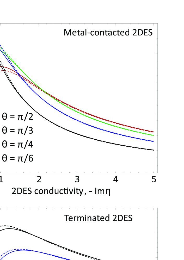
An explicit evaluation of the residue at results in the following expressions for plasmon amplitude for terminated 2DES
| (15) |
and metal-contacted 2DES
| (16) |
The photon-to-plasmon conversion coefficients (15,16) are shown in Fig. 3 as a function of at varios angles of incidence . The dissipative part of conductivity is hereby assumed very small, . The conversion coefficients approach zero for small conductivity linearly (for metal-contacted 2DES) and quadratically (for terminated 2DES). This scaling can be shown analytically by recalling that all dielectric functions approach unity as . In this limit, we find
| (17) | |||
| (18) |
These asymptotes, shown in Fig. 3 with dashed lines near the origin, agree well with full computed conversion coefficients in the limit .
We finally provide the conversion coefficients in the opposite limit . The complexity lies in evaluation of factorized functions at and . These functions are now largely different from unity, while the integrand in Cauchy factorization (4) is full of singularities. To cope with the problem, we upraise all zeros and singularities from the definition of dielectric function:
| (19) | |||
| (20) |
The Cauchy factorization of a zero-free non-singular function is much simpler. Moreover, if we are interested only in the absolute value of plasmon amplitude, ignoring the phase, only a selected section of Cauchy integral should be considered, namely
| (21) |
| (22) |
Asymptotic values of plasmon amplitude obtained with above approximate technique agree very well with those computed exactly. Surprisingly, the approximate scheme works fine even for , as shown in Fig. 3 with dashed lines.
In conclusion, we compare the peculiarities of TE-wave diffraction with those of TM-diffraction studied previously [16]. Electric field for TM diffraction is enhanced at in a singular fashion, . Such enhancement is an aftersound of the lightning rod effect at the keen non-contacted metal edge. The lightning rod effect is polarization-selective. For electric field along an edge, it turns into field suppression by dynamic currents in metal. Strong and highly non-uniform electric field for TM polarization resulted in very large photon-to-plasmon conversion efficiency which scaled as for low surface conductivity. Relative smoothness of diffracted field for TE-polarization results in moderate amplitudes of the launched plasma waves. At , ultimate values of plasmon amplitude are reached both for terminated and metal-contacted 2DES. While all electric field components in the considered polarizations remain finite, the magnetic field (being proportional to electric gradients) diverges in the vicinity of terminated edge. This can result in high efficiency of 2d magnon launching [26, 27], as well as to the local enhancement of electron spin resonance signals [28].
The presented analytical method is readily generalized to the 2DES located above perfect conductors (gates). This is acieved via replacements , where is the distance to the gate. With such a modification, it will be possible to study the hybridization of TE plasmons with cavity modes formed between 2DES and its gate [29]. Previous studies of scattering problems in such spatially non-uniform gated 2DES were limited to the weak non-locality approxiations [30, 31].
The current study dealt with an electromagnetic scattering problem. Another class of EM problems deals with the properties of edge eigenmodes [32, 33, 25], which remain largely unexplored for capacitive materials with . The edge TE plasmons, if exist, would have two non-trivial components of electric field. This would complicate the Wiener-Hopf analysis of the spectra [34]. Fortunately, efficient factorization methods for such matrix-type Wiener-Hops systems have recently emerged [35].
All our consideration relied on the local model of 2DES conductivity. This is justified by relative smoothness of emerging fields, least in the limit . An interesting aspect of conduction non-locality in TE polarization is the possible launching of shear waves [36, 37]. Such waves can propagate due to electron viscosity normally to the junction; the non-uniformity of the diffracted field provides the necessary momentum. Therefore, metal-2DES junctions illuminated with TE-polarized waves may represent a platform for studies of exotic shear excitations.
The obtained solution for local fields generated upon diffraction at the junction can be used as a building block for modeling of 2d photodetectors. The underlying light-to-current conversion mechanism can be photo-thermoelectric effect [6], photovoltaic effect [5], or photon drag [38, 39]. In all these cases, the photocurrent is a known quadratic functional of the local eclectic fields, whose particular values can be computed with our main Eqs. (6). Such scheme of photocurrent computation is simpler and more transparent than EM simulations used previously [4, 9]. It can also provide analytical insights into the limiting performance of 2d optoelectronic devices.
The work was supported by the grant # 21-79-20225 of the Russian Science Foundation.
References
- Tielrooij et al. [2015a] K. J. Tielrooij, L. Piatkowski, M. Massicotte, A. Woessner, Q. Ma, Y. Lee, K. S. Myhro, C. N. Lau, P. Jarillo-Herrero, N. F. van Hulst, and F. H. L. Koppens, Generation of photovoltage in graphene on a femtosecond timescale through efficient carrier heating, Nature Nanotechnology 10, 437 (2015a), 1504.06487 .
- Muravev and Kukushkin [2012] V. M. Muravev and I. V. Kukushkin, Plasmonic detector/spectrometer of subterahertz radiation based on two-dimensional electron system with embedded defect, Applied Physics Letters 100, 082102 (2012).
- Titova et al. [2023] E. Titova, D. Mylnikov, M. Kashchenko, I. Safonov, S. Zhukov, K. Dzhikirba, K. S. Novoselov, D. A. Bandurin, G. Alymov, and D. Svintsov, Ultralow-noise Terahertz Detection by p–n Junctions in Gapped Bilayer Graphene, ACS Nano 17, 8223 (2023), 2212.05352 .
- Olbrich et al. [2016] P. Olbrich, J. Kamann, M. König, J. Munzert, L. Tutsch, J. Eroms, D. Weiss, M.-H. Liu, L. E. Golub, E. L. Ivchenko, V. V. Popov, D. V. Fateev, K. V. Mashinsky, F. Fromm, T. Seyller, and S. D. Ganichev, Terahertz ratchet effects in graphene with a lateral superlattice, Physical Review B 93, 075422 (2016), 1510.07946 .
- Echtermeyer et al. [2014] T. J. Echtermeyer, P. S. Nene, M. Trushin, R. V. Gorbachev, A. L. Eiden, S. Milana, Z. Sun, J. Schliemann, E. Lidorikis, K. S. Novoselov, and A. C. Ferrari, Photothermoelectric and photoelectric contributions to light detection in metal-graphene-metal photodetectors, Nano Letters 14, 3733 (2014), 1402.1266 .
- Song et al. [2011] J. C. W. Song, M. S. Rudner, C. M. Marcus, and L. S. Levitov, Hot Carrier Transport and Photocurrent Response in Graphene, Nano Letters 11, 4688 (2011), 1105.1142 .
- Nalitov et al. [2012] A. V. Nalitov, L. E. Golub, and E. L. Ivchenko, Ratchet effects in two-dimensional systems with a lateral periodic potential, Phys. Rev. B 86, 115301 (2012).
- Mönch et al. [2022] E. Mönch, S. O. Potashin, K. Lindner, I. Yahniuk, L. E. Golub, V. Y. Kachorovskii, V. V. Bel’kov, R. Huber, K. Watanabe, T. Taniguchi, J. Eroms, D. Weiss, and S. D. Ganichev, Ratchet effect in spatially modulated bilayer graphene: Signature of hydrodynamic transport, Phys. Rev. B 105, 045404 (2022).
- Fateev et al. [2017] D. V. Fateev, K. V. Mashinsky, and V. V. Popov, Terahertz plasmonic rectification in a spatially periodic graphene, Applied Physics Letters 110, 061106 (2017).
- Fateev et al. [2010] D. V. Fateev, V. V. Popov, and M. S. Shur, Transformation of the plasmon spectrum in a grating-gate transistor structure with spatially modulated two-dimensional electron channel, Semiconductors 44, 1406 (2010).
- Aizin and Dyer [2012] G. R. Aizin and G. C. Dyer, Transmission line theory of collective plasma excitations in periodic two-dimensional electron systems: Finite plasmonic crystals and Tamm states, Physical Review B 86, 235316 (2012).
- Gorbenko and Kachorovskii [2024] I. Gorbenko and V. Kachorovskii, Lateral plasmonic crystals: Tunability, dark modes, and weak-to-strong coupling transition, Phys. Rev. B 110, 155406 (2024).
- Margetis et al. [2017] D. Margetis, M. Maier, and M. Luskin, On the Wiener–Hopf Method for Surface Plasmons: Diffraction from Semiinfinite Metamaterial Sheet, Studies in Applied Mathematics 139, 599 (2017).
- Zhang et al. [2014] L. Zhang, X. L. Fu, and J. Z. Yang, Excitation of propagating plasmons in semi-infinite graphene layer by free space photons, Communications in Theoretical Physics 61, 751 (2014).
- Rejaei and Khavasi [2015] B. Rejaei and A. Khavasi, Scattering of surface plasmons on graphene by a discontinuity in surface conductivity, Journal of Optics 17, 075002 (2015).
- Nikulin et al. [2021] E. Nikulin, D. Mylnikov, D. Bandurin, and D. Svintsov, Edge diffraction, plasmon launching, and universal absorption enhancement in two-dimensional junctions, Physical Review B 103, 085306 (2021).
- Svintsov and Alymov [2023] D. A. Svintsov and G. V. Alymov, Refraction laws for two-dimensional plasmons, Physical Review B 108, L121410 (2023).
- Tielrooij et al. [2015b] K. J. Tielrooij, M. Massicotte, L. Piatkowski, A. Woessner, Q. Ma, P. Jarillo-Herrero, N. F. van Hulst, and F. H. L. Koppens, Hot-carrier photocurrent effects at graphene–metal interfaces, Journal of Physics: Condensed Matter 27, 164207 (2015b), 1411.5665 .
- Semkin et al. [2022] V. Semkin, D. Mylnikov, E. Titova, S. Zhukov, and D. Svintsov, Gate-controlled polarization-resolving mid-infrared detection at metal–graphene junctions, Applied Physics Letters 120, 191107 (2022).
- Semkin et al. [2023] V. A. Semkin, A. V. Shabanov, D. A. Mylnikov, M. A. Kashchenko, I. K. Domaratskiy, S. S. Zhukov, and D. A. Svintsov, Zero-Bias Photodetection in 2D Materials via Geometric Design of Contacts, Nano Letters 23, 5250 (2023).
- Wei et al. [2021] J. Wei, C. Xu, B. Dong, C. W. Qiu, and C. Lee, Mid-infrared semimetal polarization detectors with configurable polarity transition, Nature Photonics 15, 614 (2021).
- Mikhailov and Ziegler [2007] S. A. Mikhailov and K. Ziegler, New electromagnetic mode in graphene, Phys. Rev. Lett. 99, 016803 (2007).
- Kotov and Lozovik [2016] O. V. Kotov and Y. E. Lozovik, Dielectric response and novel electromagnetic modes in three-dimensional dirac semimetal films, Phys. Rev. B 93, 235417 (2016).
- Menabde et al. [2016] S. G. Menabde, D. R. Mason, E. E. Kornev, C. Lee, and N. Park, Direct optical probing of transverse electric mode in graphene, Scientific reports 6, 21523 (2016).
- Margetis et al. [2020] D. Margetis, M. Maier, T. Stauber, T. Low, and M. Luskin, Nonretarded edge plasmon-polaritons in anisotropic two-dimensional materials, Journal of Physics A: Mathematical and Theoretical 53, 055201 (2020), 1910.04840 .
- Cenker et al. [2021] J. Cenker, B. Huang, N. Suri, P. Thijssen, A. Miller, T. Song, T. Taniguchi, K. Watanabe, M. A. McGuire, D. Xiao, and X. Xu, Direct observation of two-dimensional magnons in atomically thin CrI3, Nature Physics 17, 20 (2021).
- Safin et al. [2020] A. Safin, S. Nikitov, A. Kirilyuk, D. Kalyabin, A. Sadovnikov, P. Stremoukhov, M. Logunov, and P. Popov, Excitation of terahertz magnons in antiferromagnetic nanostructures: Theory and experiment, Journal of Experimental and Theoretical Physics 131, 71 (2020).
- Shchepetilnikov et al. [2021] A. V. Shchepetilnikov, A. R. Khisameeva, Y. A. Nefyodov, and I. V. Kukushkin, Electron spin resonance under conditions of a ferromagnetic phase transition, JETP Letters 113, 657 (2021).
- Shuvaev et al. [2022] A. Shuvaev, K. R. Dzhikirba, A. S. Astrakhantseva, P. A. Gusikhin, I. V. Kukushkin, and V. M. Muravev, Plasmonic metasurface created by a grating of two-dimensional electron strips on a substrate, Phys. Rev. B 106, L161411 (2022).
- Rodionov and Zagorodnev [2023] D. Rodionov and I. Zagorodnev, Plasmons in a strip with an anisotropic two-dimensional electron gas fully screened by a metal gate, JETP Letters 118, 100 (2023).
- Zagorodnev et al. [2023] I. V. Zagorodnev, A. A. Zabolotnykh, D. A. Rodionov, and V. A. Volkov, Two-dimensional plasmons in laterally confined 2d electron systems, Nanomaterials 13, 975 (2023).
- Volkov and Mikhailov [1988] V. Volkov and S. A. Mikhailov, Edge magnetoplasmons: low frequency weakly damped excitations in inhomogeneous two-dimensional electron systems, Sov. Phys. JETP 67, 1639 (1988).
- Sokolik et al. [2021] A. A. Sokolik, O. V. Kotov, and Y. E. Lozovik, Plasmonic modes at inclined edges of anisotropic two-dimensional materials, Phys. Rev. B 103, 155402 (2021).
- Zabolotnykh and Volkov [2016] A. A. Zabolotnykh and V. Volkov, Edge plasmon polaritons on a half-plane, JETP letters 104, 411 (2016).
- Daniele and Zich [2014] V. G. Daniele and R. Zich, The Wiener-Hopf method in electromagnetics (SciTech Publishing Incorporated, 2014).
- Afanasiev et al. [2023] A. N. Afanasiev, P. S. Alekseev, A. A. Greshnov, and M. A. Semina, Shear bernstein modes in a two-dimensional electron liquid, Phys. Rev. B 108, 235124 (2023).
- Semenyakin and Falkovich [2018] M. Semenyakin and G. Falkovich, Alternating currents and shear waves in viscous electronics, Phys. Rev. B 97, 085127 (2018).
- Gunyaga et al. [2023] A. A. Gunyaga, M. V. Durnev, and S. A. Tarasenko, Photocurrents induced by structured light, Phys. Rev. B 108, 115402 (2023).
- Entin et al. [2010] M. V. Entin, L. I. Magarill, and D. L. Shepelyansky, Theory of resonant photon drag in monolayer graphene, Phys. Rev. B 81, 165441 (2010).