Hole Capture-Structural Relaxation Mechanism of Defect Generation in Ionizing-irradiated -SiO2
Abstract
The permanent ionization damage of semiconductor devices in harsh radiation environments stems from defect centers generation in the -SiO2 dielectric or isolation layers, but the long-standing “hole transport-trapping” generation mechanism encounters dilemmas to explain recent experiments. In this work, we propose a new “hole capture-structural relaxation” (HCSR) mechanism, based on spin-polarized first-principles calculations of oxygen vacancies (’s) in -SiO2. It is found that due to an electronic metastability caused by the localization of defect electronic states, the previously suggested puckered precursor, , cannot exist in -SiO2, and the centers can arise from a structural relaxation of dimer after nonradiative capture of irradiation-induced valence band holes. We demonstrate that, such an HCSR mechanism can consistently explain the basic but puzzling temperature and electric-field dependences in recent experiments. Moreover, by using reaction rate theory, we derive an analytical formula to uniformly describe the sublinear experimental data over a wide dose and temperature range. This work not only provides a rationale for defect generation in ionizing-irradiated -SiO2, but also offer a general approach to understanding the irradiation physics in alternative dielectrics and wide-band gap semiconductors with intrinsic electronic metastability.
Introduction.– Due to its easy growth and excellent insulating properties, thermally oxidized wide-band-gap (WBG) oxides such as amorphous silicon dioxide (-SiO2) is used as dielectric or isolation layers (DIL) in various semiconductor devices based on the traditional Si [1], and emerging two-dimensional (2D) materials [2, 3] or WBG SiC [4]. These devices suffer from permanent total ionizing dose (TID) damages (e.g., shifts of threshold voltages and increases in leakage currents) when used in outer space, nuclear reactor, or particle-accelerator applications. This is because centers, i.e., positively-charged oxygen vacancies () of puckered configuration [5], are induced in the -SiO2 layer by persistent ionizing irradiations of high-energy photons and particles [6, 7, 8, 9]. The centers can also transform into centers, amphoteric Si dangling bonds at the -SiO2/Si interface, through a two-stage proton process [6, 9]. Therefore, revealing the fundamental generation mechanism of is at the heart of assessing the reliability of semiconductor devices with -SiO2 DIL in harsh radiation environments. On the other hand, -SiO2 has an ultra WBG of about 9.0 eV. Studying the defect generation mechanism in it will be instructive for understanding the defect physics in other WBG materials.
A “hole transport-trapping” mechanism has been proposed 4 decades ago to explain the generation of , based on a short-term recovery phenomena of flat-band voltages in pulse-irradiated metal-oxide-semiconductor (MOS) devices [6, 7, 8, 9]. It is suggested that, the centers are generated because holes (h+) induced by the ionizing irradiation and transported through shallow localized states in -SiO2 [10, 11] are trapped by deep defect precursors near the -SiO2/Si interface [6, 7], , see Fig. 1(a). Such a mechanism is supported by previous non-spin polarized first-principles calculations [12, 13], which identified the shallow and deep localized states as neutral of dimer and puckered configuration, and , respectively. This traditional mechanism has been widely applied, not only to various semiconductor devices with SiO2 DIL, which undergo size scaling and architecture innovation driven by Moore’s Law [8, 9], but also to many other devices made of alternative dielectrics [14] such as HfO2 [15] and ion gel [16], and WBG functional oxides such as TaOx [17]. The mechanism is so popular that, a concept of effective trapping efficiency has been proposed to use -SiO2 as a standard to evaluate the radiation resistance of alternative dielectrics [18].
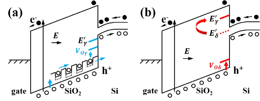
However, this long-standing “hole transport-trapping” mechanism encounters dilemmas to explain the basic experiments on temperature () and electric-field () dependence of generation dynamics, when more accurate measurements become available nowadays. As the hole trapping on both kinds of ’s are barrierless [19, 20], the buildup dynamics of in this traditional mechanism is limited by the much slower hole transport process [8, 9]. Therefore, the defect concentration, , should display and dependence determined by the hole transport process. Previous experiments demonstrated that, at above 160 K, the hole transport is strongly temperature activated with an activation energy of 0.4 eV, and the time to transport the same number of holes decays exponentially as increases, , where is the Boltzmann constant [10, 11]. Considering that is raised from room temperature (, 25∘C) to 150∘C, will be shorten by about 100 times. However, only a 3-fold shortening is observed for the time to generate the same number of centers as is raised from to 150∘C [21, 22]. Moreover, these experiments also show that, the decreases sharply as increases because the holes migrate faster to the -SiO2/Si interface [10, 11]. As the irradiation-induced hole density in the valence band (VB) of -SiO2 is also enlarged at large [23], for a same irradiation time should increase monotonically with the strength of . However, it is observed that the displays a first increase and then decrease behavior as increases [24]. These observed much weaker dependence and opposite dependence of buildup relative to the hole transport suggest that, the in ionizing-irradiated -SiO2 is hard to generate from the traditional hole transport(-trapping) mechanism.
In this work, we propose a more reasonable “hole capture-structural relaxation” (HCSR) mechanism, as illustrated in Fig. 1(b), based on spin-polarized first-principles calculations of carrier capture properties and thermal stabilities of ’s in -SiO2. It is found that, due to strong electron-phonon coupling between electronic states, the shallow can capture irradiation-induced holes in the VB of -SiO2 and transform to even at . On the other hand, due to an electronic metastability caused by the localization of defect electronic states, the dimer can easily relax to the puckered , while the traditionally assumed precursors of centers cannot survive in thermally-grown -SiO2. We demonstrate that, such a new HCSR mechanism can consistently explain the puzzling and dependences. We also derive an analytical formula based on the reaction rate theory [25], and show that it can uniformly describe the sublinear experimental data over a wide dose and range. The proposed HCSR mechanism is expected to be general in alternative dielectrics and WBG semiconductors due to their intrinsic electronic metastability [26, 27, 28, 29, 30].
Mechanism identification method.– Previous first-principles calculations use single defect levels to support the shallow-level transport and deep-level trapping mechanism. However, single defect levels are insufficient to describe the carrier capture properties and the thermal stabilities of the defect and precursor states. Here, the structures, formation energies, transition levels, and carrier capture cross-sections of ’s of neutral and positive charge states in -SiO2 are calculated to determine their thermal stabilities and carrier capture properties, and thus to reveal the generation mechanism of centers.
Our first-principles calculations of electronic structure and total energy are carried out using spin-polarized density-functional theory (DFT), as implemented in the PWmat package [31] with the NCPP-SG15-PBE pseudopotentials [32, 33, 34]. To improve the accuracy, the Heyd-Scuseria-Ernzerhof (HSE06) hybrid functional method [35] with a mixing parameter of 50% is employed. A 216-atom supercell is employed to study the properties of ’s in -SiO2. All atoms within the supercell are relaxed until the forces on each atom fall below 0.01 eV/Å and the plane-wave energy cutoff for the basis-functions is set to be 60 Ry. To obtain the carrier capture properties of ’s, the electron-phonon coupling constant are calculated using the static coupling approximation [36] and is obtained within one self-consistent field calculation [31, 37, 38]. The capture cross-section can be calculated by [39],
| (1) |
Here is the supercell volume and 0.58 (0.3 ) is the effective mass of hole (electron) in -SiO2 ( is the mass of free electron) [40]. is the structural relaxation energy between initial and final configurations after the transition from electronic states and ; is the electron-phonon coupling constant between electronic states and , as well as phonon mode ; is the frequency of the -th harmonic phonon mode. is the thermal barrier for crossing to different charge states of the same configuration. More detailed description of the calculation methods can be found elsewhere [41], in which we focus on the mechanism of substantial nonradiative carrier recombination in WBG materials (taking -SiO2 as an example) when the initial and final states have reached equilibrium. Here, the buildup process far from the equilibrium is considered.
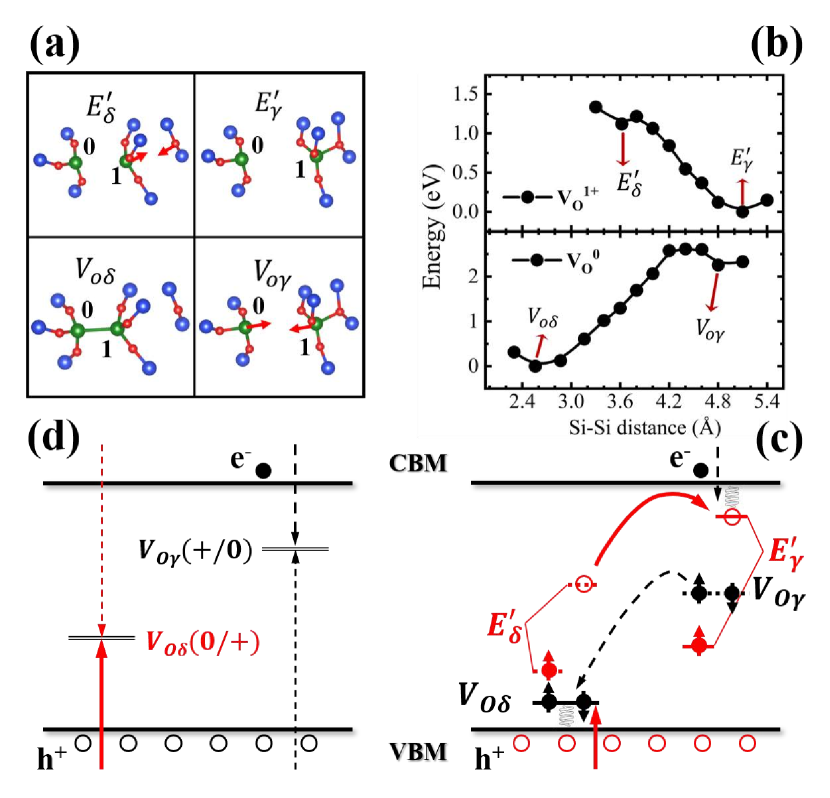
Calculation results and the HCSR mechanism.– As an amorphous material, the local bonding in -SiO2 can vary, and a typical calculation result is present in Fig. 2. From Fig. 2(a), it is clear that, consistent with previous calculations [42, 43], in -SiO2 can take two distinct local configurations for each charge state, namely dimer and puckered for neutral state, and and for positively charged state.
From the single defect levels of ’s in Fig. 2(c), it is seen that, both and are indeed very deep in -SiO2 and is relatively shallow. [ () has an empty single electron energy state about 3.68 eV (1.24 eV) below the conduction band minimum (CBM) of -SiO2. Both are much closer to the CBM than previous results [12, 13] due to spin polarization, see Fig. 1.] Therefore, it seems natural to propose the traditional mechanism: the deep prefer to trap holes around it transported through the shallow state to generate the centers of the same configuration [Fig. 1(a)]. However, rather than these single defect levels, the transition levels of ’s are more relevant to the charge capture and generation in -SiO2. Meanwhile, formation energies are necessary to justify the thermal stabilities of defect and precursor states.
The formation energies as a function of the distance between Si0 and Si1 are present in Fig. 2(b), and the locally stable structures are plotted in Fig. 2(a). It is found that, the neutral is stable because a bond is formed between Si0 and Si1. However, it becomes metastable in the positively-charged state, because the dimer bond is weakened after one electron is removed from the bond and Si1 feels Coulomb attraction from neighboring O ions (denoted by the red arrows). When Si1 relax through the base plane of three O atoms and bonds with another network O atom, a stable puckered is formed. Finally, it becomes metastable in the neutral state because the added electron form a dipole structure; Si0 with an electron and Si1 with a hole can attract each other and bond again (see the red arrows). These electronic metastabilities of and stem from a strong localization of defect electronic states. As seen in Fig. 2(b), the metastable () is about 1.1 eV (2.2 eV) higher in total energy than the stable () and can transform to the latter by overcoming a small barrier of 0.11 eV (0.35 eV). Assuming an attempt frequency of 1013s-1 [44], we estimate that the time to transform from to is approximately 1 ns, and to transform from to is about 70 ns.
These calculation results have important implications to reveal the generation mechanism in ionizing-irradiated -SiO2 DIL. First, the -SiO2 DIL in modern semiconductor devices are prepared by thermal oxidation process at typical high temperature of 800∘C1100∘C. Thus, the small relaxation barrier of means that , the previously suggested precursors of , cannot exist in -SiO2. Therefore, are unlikely to be generated from the traditional mechanism. Second, the quick structural relaxation has been observed in hole injection experiments [45]. Since the metastable stems from hole addition to the stable , it can be inferred that, the stable may be generated from VB-hole capture on and subsequent structural relaxation,
| (2) |
This new HCSR mechanism is illustrated in Fig. 2(c) and Fig. 1(b). It would require easy hole capture on and hard electron capture on the resulting at .
The transition level and capture cross-sections of ’s in -SiO2 are calculated to close this issue. Note that, these calculations of nonradiative capture has long been difficult, until Wang et al. develop a novel approach to reduce the computational cost to include all phonon modes [37, 38]. In Fig. 2 (d), the transition energy levels are found at 3.5 eV above the VBM and 2.2 eV below the CBM, for the dimer and puckered configuration, respectively. The stable is found to have a large at , not only because it has a relatively shallow energy level thus a large overlap with the wave function of the VBM, but also because it has a large structural relaxation energy (2.5 eV) comparable to the transition energy level (3.5 eV). These factors respectively lead to a strong between and electronic states, and a small of about 0.09 eV in Eq. (1). The resulting metastable state is found to have a negligible smaller than , because the transition level is too deep to capture electrons from the CB of -SiO2. These calculated results mean that, can easily capture the irradiation-induced VB holes even at room temperature, and the resulting centers will not turn back by trapping the irradiation-induced CB electrons, but will quickly deform to the stable centers, as suggested in Eq. (2). Therefore, we have attained a new HCSR mechanism for the charge trapping and defect generation in ionizing-irradiated -SiO2 DIL, see Fig. 1(b) and Fig. 2(c).
With high mobility, much fewer CB electrons than VB holes are present in ionizing-irradiated -SiO2 [6, 7]. Meanwhile, the stable is found to have a at that is much smaller than . (The metastable state has a negligible smaller than .) Therefore, the generated is hard to be eliminated by the irradiation-induced CB electrons, and will be continuously build-up through the HCSR process. However, if the initial and final states have reached equilibrium, the electron capture on [with an end of due to structural relaxation of the resulting , see black arrows in Fig. 2(c)] becomes as fast as the hole capture on , and a substantial nonradiative recombination can arise in -SiO2, called as a dual-level enhanced recombination in WBG semiconductors [41, 46].
The above analyses show that, the electronic metastability of and play an essential role in our proposed HCSR mechanism. As the electronic metastability commonly exists in alternative dielectrics (HfO2, Al2O3, h-BN, etc.) and WBG semiconductors with strongly localized electronic states [26, 27, 28, 29, 30], the new mechanism is expected to be general in these materials used in harsh radiation environments.
Explanations of basic dependences.– We now demonstrate that, the basic temperature [21, 22] and electric-field [24] dependences of buildup dynamics in -SiO2, which although seem puzzling from the traditional “hole transport-trapping” mechanism, can be readily explained by our proposed HCSR mechanism. The overall buildup rate of is limited by the hole capture process, which is generally much slower than the structural relaxation process [47]. Thus, the rate constant of generation can be given by [39], where and are the thermal velocity and density [23] of holes in the -SiO2 VB, respectively. As only one percent or less of are consumed to generate for typical irradiation dose of 100 krad(Si) [43], a linear generation dynamics, , can be considered.
As in the rate constant weakly depends on [48], the dependence of at a fixed is determined by , according to Eq. (1). From the calculated small eV, it is readily derived that the at a fixed time increases only 3.4 times as increases from to 150∘C. Accordingly, the time required to produce defects of the same concentration should shrink by the same multiple. This result is very close to the experimental observations of defect dynamics [21, 22], but is much weaker than the near 100-fold shortening of observed in the hole transport dynamics [10, 11]. The dependence of at a fixed time is a product of and , because in the rate constant is independent of . As the spatial separation of irradiation-induced electron-hole pairs becomes more significant under a stronger electric field, the hole density in -SiO2 VB has a positive dependence on [23]. On the other hand, the of has a negative dependence on , because an electric field causes a tilt of the polarization potential of the neutral that is induced by holes. This effect reduces the volume of the polarization potential below a critical value that is proportional to [49, 50]. Therefore, as a product of and display a first increase and then decrease behavior at relatively small and large , respectively. This basic trend is consistent with the observation in defect dynamics [24], but is essentially different from the monotonic dependence observed in hole transport [10, 11].
Analytical formula to describe the data.– We at last derive an analytical formula of generation dynamics based on the proposed mechanism and the amorphous property of -SiO2. It can uniformly describe the sublinear experimental data over a wide range. According to the reaction rate theory [25] and Eq. (2), the annihilation rate equation of is given by . As an amorphous material, the local atomic configurations of vary in -SiO2 [12, 13], and the hole capture cross-sections of them have a wide distribution [51]. As the irradiation goes on, with relatively large becomes fewer, and the probability of hole captured by with small increases. This is a typical case of the hierarchically constrained dynamics proposed for glassy materials [52, 53]. Accordingly, the annihilation of in -SiO2 should follow a Kohlrausch stretched exponential decay [54], , instead of a conventional Debye exponential form (). Here is the initial concentration of and is a dispersion factor. Therefore, the hole-capture-limited buildup of is given by . Considering that very few are consumed to generate [43], the above result can be Taylor expanded and we obtain a concise formula of the generation dynamics in irradiated -SiO2,
| (3) |
Here , is the dose rate, and is the total dose. Note that, the and dependences of this sublinear dynamics () are slightly reduced relative to those of the previously discussed linear dynamics, but their consistencies with the experiments [21, 22, 24] do not change.
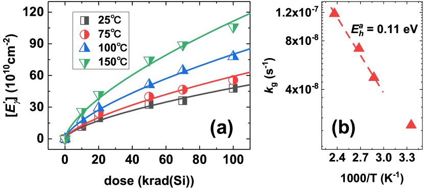
The concise formula in Eq. (3) is compared with previous experimental data [21] to demonstrate its universality. The data and fitting curves in Fig. 3(a) show that, the formula can uniformly describe the data over a wide range, which even though display significant nonlinearities and dependence. The parameters in Eq. (3) are extracted from the unified fitting. is found to be close to 2/3 for all [57], which is much larger than the dispersion factor of 0.22 for hole transport in -SiO2 [10, 11], further reflecting the irrelevance of the two dynamics. plotted in Fig. 3(b) is found to display an Arrhenius-like dependence. (With the fitted and , is calculated by setting as cm-2 [43]; it becomes smaller for larger , but the dependence is almost unaffected.) Considering the definitions of and , the thermal barrier of hole capture on can be calculated by . The value is found as 0.11 eV, which is very closed to our first-principles result (0.09 eV).
Conclusion.– In conclusion, we have proposed an HCSR mechanism and derived an analytical formula for the deep defect generation in ionizing-irradiated -SiO2, based on spin-polarized first-principles calculations on the thermal stabilities and carrier capture properties of ’s therein, and the concept of hierarchical constrained dynamics. The rationality of the mechanism has been demonstrated by consistent explanations of the confusing and dependences and unified description of the - and -dependent data. Our proposed generation mechanism should build a foundation for assessing the radiation tolerance of semiconductor devices with -SiO2 DIL in harsh radiation environments; it is also expected to be general for alternative dielectrics and other WBG semiconductors with intrinsic electronic metastability.
This work was supported by the National Natural Science Foundation of China (Nos. 11991060, 12088101, and U2230402).
References
- Prinzie et al. [2021] J. Prinzie, F. M. Simanjuntak, P. Leroux, and T. Prodromakis, Nat. Electron. 4, 243 (2021).
- Das et al. [2021] S. Das, A. Sebastian, E. Pop, C. J. McClellan, A. D. Franklin, T. Grasser, T. Knobloch, Y. Illarionov, A. V. Penumatcha, J. Appenzeller, et al., Nat. Electron. 4, 786 (2021).
- Akinwande et al. [2019] D. Akinwande, C. Huyghebaert, C.-H. Wang, M. I. Serna, S. Goossens, L.-J. Li, H.-S. P. Wong, and F. H. Koppens, Nature 573, 507 (2019).
- Alkauskas et al. [2008] A. Alkauskas, P. Broqvist, F. Devynck, and A. Pasquarello, Phys. Rev. Lett. 101, 106802 (2008).
- Lenahan and Dressendorfer [1984] P. M. Lenahan and P. Dressendorfer, J. Appl. Phys. 55, 3495 (1984).
- Oldham and McLean [2003] T. R. Oldham and F. McLean, IEEE Trans. Nucl. Sci. 50, 483 (2003).
- Schwank et al. [2008] J. R. Schwank, M. R. Shaneyfelt, D. M. Fleetwood, J. A. Felix, P. E. Dodd, P. Paillet, and V. Ferlet-Cavrois, IEEE Trans. Nucl. Sci. 55, 1833 (2008).
- Fleetwood [2017] D. M. Fleetwood, IEEE Trans. Nucl. Sci. 65, 1465 (2017).
- Fleetwood [2022] D. Fleetwood, Appl. Phys. Lett. 121, 070503 (2022).
- McLean et al. [1976] F. McLean, H. Boesch, and J. McGarrity, IEEE Trans. Nucl. Sci. 23, 1506 (1976).
- Hughes [1977] R. Hughes, Phys. Rev. B 15, 2012 (1977).
- Nicklaw et al. [2002] C. Nicklaw, Z.-Y. Lu, D. Fleetwood, R. Schrimpf, and S. Pantelides, IEEE Trans. Nucl. Sci. 49, 2667 (2002).
- Lu et al. [2002] Z.-Y. Lu, C. Nicklaw, D. Fleetwood, R. Schrimpf, and S. Pantelides, Phys. Rev. Lett. 89, 285505 (2002).
- Kingon et al. [2000] A. I. Kingon, J.-P. Maria, and S. Streiffer, Nature 406, 1032 (2000).
- Zhu et al. [2023] M. Zhu, P. Lu, X. Wang, Q. Chen, H. Zhu, Y. Zhang, J. Zhou, H. Xu, Z. Han, J. Han, et al., Small 19, 2204537 (2023).
- Zhu et al. [2020] M. Zhu, H. Xiao, G. Yan, P. Sun, J. Jiang, Z. Cui, J. Zhao, Z. Zhang, and L.-M. Peng, Nat. Electron. 3, 622 (2020).
- Zhang et al. [2011] L. Zhang, R. Huang, D. Gao, P. Yue, P. Tang, F. Tan, Y. Cai, and Y. Wang, IEEE T Electron Dev. 58, 2800 (2011).
- Felix et al. [2002] J. Felix, D. Fleetwood, R. Schrimpf, J. Hong, G. Lucovsky, J. Schwank, and M. Shaneyfelt, IEEE Trans. Nucl. Sci. 49, 3191 (2002).
- Rowsey et al. [2011] N. L. Rowsey, M. E. Law, R. D. Schrimpf, D. M. Fleetwood, B. R. Tuttle, and S. T. Pantelides, IEEE Trans. Nucl. Sci. 58, 2937 (2011).
- Hughart et al. [2012] D. Hughart, R. Schrimpf, D. Fleetwood, N. Rowsey, M. Law, B. Tuttle, and S. Pantelides, IEEE Trans. Nucl. Sci. 59, 3087 (2012).
- Dong et al. [2020] L. Dong, J. Yang, X. Yu, G. Lv, Y. Fan, and X. Li, IEEE Trans. Nucl. Sci. 67, 2003 (2020).
- Witczak et al. [1997] S. Witczak, R. Schrimpf, D. Fleetwood, K. Galloway, R. Lacoe, D. Mayer, J. M. Puhl, R. Pease, and J. S. Suehle, IEEE Trans. Nucl. Sci. 44, 1989 (1997).
- Johnston et al. [2014] A. Johnston, R. Swimm, D. Thorbourn, P. Adell, and B. Rax, IEEE Trans. Nucl. Sci. 61, 2818 (2014).
- Shaneyfelt et al. [1990] M. Shaneyfelt, J. Schwank, D. Fleetwood, P. Winokur, K. Hughes, and F. Sexton, IEEE Trans. Nucl. Sci. 37, 1632 (1990).
- Hänggi et al. [1990] P. Hänggi, P. Talkner, and M. Borkovec, Rev. Mod. Phys. 62, 251 (1990).
- Momida and Ohno [2020] H. Momida and T. Ohno, Appl. Phys. Lett. 117, 103504 (2020).
- Zobelli et al. [2007] A. Zobelli, C. Ewels, A. Gloter, and G. Seifert, Phys. Rev. B 75, 094104 (2007).
- Park and Chadi [1999] C. Park and D. Chadi, Phys. Rev. Lett. 82, 113 (1999).
- Park et al. [2002] C. Park, S. Zhang, and S.-H. Wei, Phys. Rev. B 66, 073202 (2002).
- Li et al. [2005] J. Li, S.-H. Wei, and L.-W. Wang, Phys. Rev. Lett. 94, 185501 (2005).
- Wang [2019] L. Wang, J. Semicond. 40, 091101 (2019).
- Jia et al. [2013a] W. Jia, J. Fu, Z. Cao, L. Wang, X. Chi, W. Gao, and L.-W. Wang, J. Comput. Phys. 251, 102 (2013a).
- Jia et al. [2013b] W. Jia, Z. Cao, L. Wang, J. Fu, X. Chi, W. Gao, and L.-W. Wang, Comput. Phys. Commun. 184, 9 (2013b).
- Schmidt et al. [2012] S. S. Schmidt, D. Abou-Ras, S. Sadewasser, W. Yin, C. Feng, and Y. Yan, Phys. Rev. Lett. 109, 095506 (2012).
- Heyd et al. [2003] J. Heyd, G. E. Scuseria, and M. Ernzerhof, J. Chem. Phys. 118, 8207 (2003).
- Pässler [1982] R. Pässler, Czechoslov. J. Phys. B 32, 846 (1982).
- Shi and Wang [2012] L. Shi and L.-W. Wang, Phys. Rev. Lett. 109, 245501 (2012).
- Shi et al. [2015] L. Shi, K. Xu, and L.-W. Wang, Phys. Rev. B 91, 205315 (2015).
- Huang [1981] K. Huang, Contemp. Phys. 22, 599 (1981).
- Kumar Chanana [2011] R. Kumar Chanana, J. Appl. Phys 109 (2011).
- Qiu et al. [2023] C. Qiu, Y. Song, H.-X. Deng, and S.-H. Wei, J. Am. Chem. Soc. 145, 24952 (2023).
- Boero et al. [1997] M. Boero, A. Pasquarello, J. Sarnthein, and R. Car, Phys. Rev. Lett. 78, 887 (1997).
- Blöchl [2000] P. E. Blöchl, Phys. Rev. B 62, 6158 (2000).
- Grasser et al. [2011] T. Grasser, B. Kaczer, W. Goes, H. Reisinger, T. Aichinger, P. Hehenberger, P.-J. Wagner, F. Schanovsky, J. Franco, M. T. T. Luque, et al., IEEE T Electron Dev. 58, 3652 (2011).
- Warren et al. [1994] W. Warren, M. Shaneyfelt, D. Fleetwood, J. Schwank, P. Winokur, and R. Devine, IEEE Trans. Nucl. Sci. 41, 1817 (1994).
- Yang et al. [2016] J.-H. Yang, L. Shi, L.-W. Wang, and S.-H. Wei, Sci. Rep. 6, 21712 (2016).
- Weeks et al. [1975] J. D. Weeks, J. C. Tully, and L. Kimerling, Phys. Rev. B 12, 3286 (1975).
- Taylor and Al-Jassar [1984] D. Taylor and A. Al-Jassar, Journal of Physics D: Applied Physics 17, 819 (1984).
- Dussel and Böer [1970] G. Dussel and K. Böer, phys. status solidi (b) 39, 375 (1970).
- Lax [1960] M. Lax, Phys. Rev. 119, 1502 (1960).
- Tzou et al. [1983] J. J. Tzou, J. Y.-C. Sun, and C.-T. Sah, Appl. Phys. Lett. 43, 861 (1983).
- Palmer et al. [1984] R. G. Palmer, D. L. Stein, E. Abrahams, and P. W. Anderson, Phys. Rev. Lett. 53, 958 (1984).
- Berthier and Biroli [2011] L. Berthier and G. Biroli, Rev. Mod. Phys. 83, 587 (2011).
- Kohlrausch [1854] R. Kohlrausch, Ann. Phys. 167, 179 (1854).
- Chang et al. [1986] S. Chang, J. Wu, and S. Lyon, Appl. Phys. Lett. 48, 662 (1986).
- Stahlbush et al. [1993] R. Stahlbush, A. Edwards, D. Griscom, and B. Mrstik, J. Appl. Phys. 73, 658 (1993).
- Winokur and Boesch [1980] P. Winokur and H. Boesch, IEEE Trans. Nucl. Sci. 27, 1647 (1980).