Characterizing the chemical potential disorder in the topological insulator (Bi1-xSbx)2Te3 thin films
Abstract
We use scanning tunneling microscopy and spectroscopy under ultra-high vacuum and down to 1.7 K to study the local variations of the chemical potential on the surface of the topological insulator (Bi1-xSbx)2Te3 thin films (thickness 7 – 30 nm) with varying Sb-concentration , to gain insight into the charge puddles formed in thin films of a compensated topological insulator. We found that the amplitude of the potential fluctuations, , is between 5 to 14 meV for quasi-bulk conducting films and about 30 – 40 meV for bulk-insulating films. The length scale of the fluctuations, , was found to span the range of 13 – 54 nm, with no clear correlation with . Applying a magnetic field normal to the surface, we observe the condensation of the two-dimensional topological surface state into Landau levels and find a weak but positive correlation between and the spectral width of the Landau-level peaks, which suggests that quantum smearing from drift motion is the source of the Landau level broadening. Our systematic measurements give useful guidelines for realizing thin films with an acceptable level of potential fluctuations. In particular, we found that realizes the situation where shows a comparatively small value of 14 meV and the Dirac point lies within 10 meV of the Fermi energy.
I Introduction
Inducing superconductivity in a topological insulator (TI) by the proximity effect is a promising way to realize topological superconductivity (TSC) [1]. In particular, when a bulk-insulating 3D TI is confined to a quasi-one-dimensional nanowire, the topological surface state (TSS) breaks into peculiar subbands, which, when proximitized by a conventional superconductor, can host Majorana zero modes [2]. However, while the typical subband spacing in TI nanowires is of the order of meV, the chemical potential at the surface of 3D bulk TIs varies by tens of meV due to disorder [3, 4, 5, 6, 7, 8, 9, 10, 11]. Indeed, recent calculations [12, 13] suggest that typical impurity concentrations of the order of \qty1e19\per\cubic\centi are already sufficient to obscure any subband signatures in transport properties of TI nanowires.
In 2D TIs, the chemical potential fluctuations due to disorder lead to the formation of charge puddles in the insulating 2D bulk, which influences the transport properties of metallic 1D edge states in many ways: In HgTe quantum well [14, 15], in InAs/InGaSb [16], and in V-doped (Bi1-xSbx)2Te3 [17], the charge puddles are believed to be responsible for a reduction of the group velocity of the edge state. In another experiment on HgTe quantum well in magnetic fields [18], it was proposed that an accumulation of bulk puddles at the edge of the 2D bulk supports a chiral quantum Hall edge channel coexisting with the helical edge channel and leads to a finite (and opposite) conductance. In the case of quantum anomalous Hall insulators that are realized in ferromagnetic TI films, the charge puddles increase the localization length of the chiral edge state [19] or are responsible for the breakdown of the quantum anomalous Hall effect [20]. It is clear from these studies that precise information on the charge puddles in thin TI materials is indispensable for understanding their transport properties.
Experimentally, scanning tunneling microscopy and spectroscopy (STM/STS), which allows real space mapping of the variations in the electrical potential with sub-nanometer spatial and sub-meV energy resolution, has been employed to study the disorder effects on prototypical TI materials such as , , and . These STM/STS studies consistently revealed chemical potential fluctuations of about 10 – 60 meV over a typical length scale of about 10 – 60 nm at the surface of bulk crystals [3, 4, 5, 6, 7, 8, 9, 10, 11] and nanoplatelets [21]. However, similar information for thin films is scarce [22].
In this work, we use STM/STS under ultra-high vacuum (UHV), at 1.7 K and out-of-plane magnetic fields up to 9 T to study the local variations of the chemical potential at the surface of (Bi1-xSbx)2Te3 thin films grown on sapphire [Al2O3(0001)]. To see the possible effect of screening due to a superconductor at the bottom of the film, we also measured (Bi1-xSbx)2Te3 films on superconducting Nb prepared by the “flip-chip” (FC) technique [23]. Although our samples are clean enough to present clearly resolved Landau-level peaks in perpendicular magnetic fields, the observed potential fluctuations of up to 40 meV indicate that the effect of Coulomb disorder is relatively strong in (Bi1-xSbx)2Te3 thin films, particularly when the film is bulk-insulating. Nevertheless, at 0.65, one can obtain a quasi-bulk-insulating sample with a relatively low potential disorder of 14 meV.
II Experimental Methods
(Bi1-xSbx)2Te3 films were grown with the molecular beam epitaxy (MBE) technique as described previously [24, 25]. After cooling to 310 K, samples were capped by 10 – 20 nm of Te to protect the films during transfer. The Te-capped samples were removed from the MBE chamber and transferred ex-situ to the STM system. Typical transfer times are less than 5 minutes, minimizing the exposure of the capped films to ambient conditions. Inside the STM preparation chamber (pressure mbar), the samples are first outgassed at about 400 K for about 30 min, subsequently heated up to about 540 K (in about 10 min), kept at 540 K for min, and then cooled to room temperature. The pressure in the chamber before turning off the heater is typically well below mbar, such that the Te is completely evaporated. Some films were transferred from the sapphire substrate onto a superconducting Nb film using a flip-chip technique [23]: First, an amorphous Nb layer of several tens of nm was deposited onto the (Bi1-xSbx)2Te3 surface, and the top Nb surface is subsequently glued to a metallic substate to flip the film; the sample is then brought into the STM preparation chamber and the sapphire substrate is removed in UHV by cleaving, which usually occurs between the (Bi1-xSbx)2Te3 and sapphire rather than between (Bi1-xSbx)2Te3 and Nb due to the sticky nature of Nb. One can thus obtain a clean (Bi1-xSbx)2Te3 surface suitable for STM observations.
After obtaining a clean surface in the STM preparation chamber either by Te evaporation or by cleaving, the samples are transferred in-situ into the STM main chamber and cooled down. STM experiments are carried out under UHV conditions with a commercial system (Unisoku USM1300) operating at a base temperature of K unless stated otherwise. Topography and maps are recorded in the constant-current mode. Spectroscopy data is obtained by first stabilizing for a given setpoint condition and then disabling the feedback loop. spectra are then recorded using a lock-in amplifier by adding a small modulation voltage with frequency Hz to the sample bias voltage . Tips have been prepared by Ar ion sputtering (at an argon pressure of mbar and a voltage of kV), followed by repeated heating by electron bombardment ( W) for s. Further tip forming is done by scanning on the Cu(111) surface until a clean signature of the surface state is obtained in spectroscopy. Data are processed using Igor Pro.
III Basic characterizations
A typical STM topography of the surface of our (Bi1-xSbx)2Te3 film is shown in Fig. 1(a), which shows that the film has quintuple layer (QL) step heights of about 1 nm (line profile taken along the red arrows). A low surface roughness of this film is evident with only two terrace heights being visible in the entire field of view. The atomic resolution imaging shows the characteristic hexagonal lattice of the top Te-layer with a lattice spacing of about \qty4.3, that is consistent with the (Bi1-xSbx)2Te3 structure.
A typical spectrum, which is roughly proportional to the local density of states (LDoS) of the sample, is shown for = 0.5 in Fig. 1(b): The Fermi energy lies in the U-shaped minimum of the bulk band gap and the energy position of the bulk valance band top is easily recognizable as a sharp step-like increase in the spectrum at . In contrast, the energy position of the bulk conduction band bottom is more difficult to identify, as it causes a more subtle increase at . Nevertheless, by numerically calculating the derivative of the differential tunnel conductance and phenomenologically defining as the maxima in , we can objectively determine 120 meV. The same definition gives correct meV for the bulk valence band. In this film, the Dirac point lies almost exactly at the bulk valence band top as determined by Landau level spectroscopy discussed in Sec. V and the supplement [26]. We will discuss the properties of the TSS in Sec. V. The additional maxima in at lower and higher energies than and present a spacing of around 90 meV. They are attributed to the quantization of the bulk bands caused by the finite film thickness, as discussed in Appendix. A.
IV Amplitude and length scale of potential fluctuations
We employ the well-established rigid shift model [27, 3, 4] to measure the local potential disorder at the surface given as , where denotes the statistical mean. To this end, we record STS grids covering areas of with resolutions of \qtyrange16100^2, and determine and for each spectrum and calculate at each location of the grid. As shown in Appendix B, we have actually confirmed the rigid-shift nature of the position-dependent spectra. The topography simultaneously acquired with one such STS grid is shown in Fig. 2(b) and spectra from the grid at are plotted in Fig. 2(a). The spectrum taken at is the one plotted in Fig. 1(b) and serves as a reference to illustrate the rigid shift of the characteristic features at and in the spectra taken at and .
Plotting as a function of position in Fig. 2(c), one can see the spatial distribution of the potential disorder, where the extended excess-electron puddles with negative (blue) and fewer-electron puddles with positive (red) spanning tens of nanometer are conveniently illustrated. Note that these puddles are chemical potential fluctuations in a metallic background and they are different from electron and hole puddles formed in an insulating background [28], although both are caused by Coulomb impurities. We define the amplitude of the chemical potential fluctuations as the width of the Gaussian distribution fit to the histogram of as shown in Fig. 2(d) [28, 29, 30], and the typical length scale of the puddle is defined as the distance where the azimuthal average of the autocorrelation in the map of starts to decay more rapidly than , see Fig. 2(e). In the example shown here, 40 meV and 30 nm. The choice of a faster-than- decay for the definition of is motivated by the intuition that it marks the distance at which the Thomas-Fermi polarization bubble screens the charged impurities. The values defined this way are consistent with what one can infer in Fig. 2(c) as the puddle size (additional examples are given in the supplement).
V Landau levels and Dirac point
The LDoS of an idealistic massless two-dimensional Dirac cone of the TSS increases linearly with and it is in principle straightforward to determine the Dirac point energy from the linear slope of the signal inside the bulk band gap. In practice, however, complications due to a finite curvature [31, 9] and broadening of the bulk valence band top by shallow acceptor states lead to large uncertainties in determined in such a way, especially for the range where . On the other hand, Landau level spectroscopy [27, 32, 33, 34, 35, 8, 36, 31, 9, 37] is ideally suited to isolate the spectral features of the TSS by looking at the response of the LDoS to an external magnetic field applied normal to the surface.
In the case of the TSS, the eigenenergy of the -th Landau level is approximately given as
| (1) |
with the Dirac point energy and the Fermi velocity. The last term in Eq. 1 is a correction due to a finite curvature of the Dirac cone [33, 34, 35, 8, 36, 31, 37] giving rise to the effective mass . For simplicity, corrections due to the Stark-effect [5, 31] and additional effective Zeeman effect [38, 9] are disregarded.
Before measuring the magnetic-field dependence of the spectra discussed below, we typically performed a rough spatial sampling of several () positions r in the highest magnetic field, and performed the field dependence measurements at the r position where the sharpest spectrum was obtained in the sampling. As will be discussed in Sec. VII, these regions likely correspond to local extrema in the fluctuating potential.
In Fig. 3(a)-(d) we show spectra for = 0, 0.5, 0.67, and 0.96 in various magnetic fields, where well-defined peaks in the LDoS appear with increasing magnetic field. For each value, we indicate the Landau level index on the spectra taken at the highest field, and the vertical dashed line marks the position of when it is in the measured bias range. In the case of = 0 (i.e. Bi2Te3) shown in Fig. 3(a), the first Landau level resolved has the index and lies about 80 meV below the Fermi energy ; Landau levels with lower indices are completely masked by the LDoS stemming from the bulk valence band and only Landau levels with are seen in the bulk band gap. On the other hand, for shown in Fig. 3(c), even the first hole-like Landau level () is seen in the bulk-band gap and it is located at 50 meV above . In agreement with a previous study [22], we find that for [Fig. 3(b)], lies within 10 meV of and, although is slightly below , the zeroth Landau level is still not smeared by bulk carriers.
Note that the zeroth Landau level in Fig. 3(b) slightly shifts towards lower energy with increasing field, while it shifts in the opposite direction in Fig. 3(c). This magnetic-field dependence of the zeroth Landau level is not captured in Eq. 1 but is understood as an effective Zeeman effect that is proportional to the gradient of the local potential and the magnetic length squared, namely, [38, 9]. Therefore, the opposite direction of the shift in Figs. 3(b) and 3(c) suggests that the two sets of spectra should have been taken near a potential minimum and maximum, respectively.
Another effect not captured by Eq. 1 is the lifting of the degeneracy of Landau subbands with different total angular momentum (). In the first approximation, as shown by Fu et al. [31], Landau orbits with higher drift at larger and experience a larger potential , which lifts the degeneracy. This effect is likely responsible for the splitting of Landau levels with in Fig. 3(c). Additional spectra showing the splitting of Landau levels can be found in Fig. S10 of the supplement [26].
As for the dependence of the Landau levels on , we note that for , the zeroth Landau level to identify is sometimes visible [as in Fig. 3(d)] but it can also be completely masked by the bulk valence band (we measured four samples with = 0.5, see Table 1). In the latter case, we determined from Eq. 1 as shown in Fig. 3(e), where one can see that, even by neglecting the last term in Eq. 1, the experimental data can be reasonably fit with , which is in good agreement with previous studies [5, 8, 10]. Slight improvements are achieved by using the full expression (solid lines) with and ( is the free electron mass).
To analyze the line-shape, we extract the full-width at half maximum (FWHM) of each Landau level peak after subtracting a smooth background (details on the background subtraction and fitting are found in Appendix C), and the results are collected in Fig. 3(f). The FWHM of the and samples are essentially in the 3–8 meV range, which agrees well with previous reports on bulk crystals [35, 22, 36]. Moreover, as originally reported by Hanaguri et al. [35] for bulk , the Landau levels in these samples sharpen near . In particular, for , the FWHM of the peak which is located near is only 4 meV. Intriguingly, the data from the sample [black symbols in Fig. 3(f)] show a different trend: The FWHM tends to be reduced when the peaks are further away from . A similar trend was observed in bulk by Storz et al. [36], while an opposite trend, an increase in FWHM with , was reported for thin-films by Jiang et al. [34] and for bulk by Pauly et al. [8]. The origin of the complex evolution of the FWHM with energy is beyond the scope of this paper.
| Sample | x | t | Nd | |||||||
|---|---|---|---|---|---|---|---|---|---|---|
| (\unit) | (\qty1e19\per\cubic) | (meV) | (meV) | (meV) | (\qty1e5\per) | (meV) | (meV) | (\unit) | ||
| MBE4 2022 Apr07 | 0 | 17 | 1.2 | -110 | 31 | -233 | 5 | |||
| MBE4 2022 Apr28B | 0 | 12 | -114 | 47 | -169 | 4.9 | 4.4 | |||
| MBE3 2022 Oct28D2 | 0.5 | 9 | -127 | 121 | -130 | 5.2 | 7 | 40 | ||
| MBE3 2022 Oct28D2 FC∗ | 0.5 | 7 | -120 | 185 | 37 | |||||
| MBE3 2022 Oct28C2 | 0.5 | 9 | -35 | 212 | -66 | 6.2 | 8.2 | 30 | ||
| MBE3 2022 Jun6C FC∗ | 0.5 | 12 | -92 | 116 | -95 | 3.8 | 9.4 | |||
| MBE2 2020 Oct9B | 0.65 | 30 | 3 | 240 | 41 | 4.6 | 5.9 | 14 | ||
| MBE3 2022 Jun5B2 | 0.67 | 19 | 29 | 12 | 207 | 10 | 4.2 | 5.9 | ||
| MBE1 2021 Sep8 FC∗ | 0.86 | 7 | -206 | -5 | -189 | 5.1 | 10.4 | 9 | ||
| MBE3 2022 Apr13A | 0.96 | 13 | 50 | 34 | 91 | 4.4 | 6.4 | 9 |
VI -dependence of the TSS and
We have performed the analysis described in Sec. IV and Sec. V for many films with the thickness of 7 – 30 nm and values from 0 to 0.96, and the results are summarized in Table 1. One can immediately see that with increasing , the Dirac point energy shifts up in relation to both and , as plotted in Figs. 4(a) and 4(b). In agreement with the photoemission work [39], we find that the Dirac point is above the bulk valence band top for . However, as discussed above, in our Landau-level spectroscopy we find the Dirac point is only consistently well-visible for and frequently obscured in films due to the overlap with the bulk valance band. Also, in agreement with the previous STM work [22], we find the Dirac point is the closest to the Fermi level for . Interestingly, our data of are systematically shifted compared to the photoemission data [39], which may be attributed to surface band bending [33, 40, 37] or to higher growth and post-annealing temperatures which were reported to lead to more -type films [22].
Next, let us look at the -dependence of the potential disorder amplitude shown in Fig. 4(c). Interestingly, peaks at , at which is located roughly at the middle of the 200 meV bulk band gap. This suggests that reduced screening by bulk carriers enhances the strength of the disorder effect. In this regard, our samples can be roughly separated into two groups, bulk-insulating films and quasi-bulk-conducting films depending on the position of , where the former shows 30 – 40 meV while the latter shows 5 – 14 meV. Quantitatively speaking, the films fall into the latter category when is within 30 – 50 meV from a bulk band edge. There is no clear correlation between and .
Our data on the flip-chip films on Nb, whose data are also plotted in Fig. 4, show that the measured potential disorder amplitude is essentially unaffected by the superconducting Nb film of about 60 nm thickness, suggesting that the additional screening provided by the superconductor at the bottom surface leaves the top surface probed by STM largely unaffected. This is true for both the bulk-conducting film with 9 meV and the bulk-insulating film with 37 meV on Nb.
| Reference | Material | thickness | T | |||
| (\unit) | (meV) | (\unit) | () | (\unit) | ||
| Beidenkopf et al. [3] | 40 | 24 | 2 | 4 | ||
| 20 | 4 | |||||
| 20 | 4 | |||||
| Dai et al. [41] | 20 to 30∗∗ | |||||
| Okada et al. [5] | 12 | 50 | 4 | |||
| Lee et al. [7, 4] | 30 | 20 | 5 | 4.5 | ||
| Chong et al. [4, 42] | 15 | 50 | 0.3 | |||
| 0.3 | ||||||
| Pauly et al. [8] | 40 | 6 | ||||
| Fu et al. [31, 9, 9] | ||||||
| 1.5 | ||||||
| Storz et al. [10] | 15 | 40 | 4 | |||
| Knispel et al. [11] | 40-50 | |||||
| Parra et al. [21] | 8 to 30 | 2 to 30 | 6 to 15 | 78 | ||
| this work | (Bi1-xSbx)2Te3 |
VII Discussions and Conclusion
So far we have shown the existence of relatively large potential fluctuations in all of our samples. Now let us briefly discuss its origin. In (Bi1-xSbx)2Te3, the carrier density is controlled by compensation doping, where electron (hole) carriers in the bulk are minimized by countering them with compensating acceptors (donors). These acceptors and donors cause a random distribution of Coulomb impurities, leading to random potential fluctuations and creating charge puddles [29]. For a TI film of thickness , dielectric constant [11], Dirac velocity , the Dirac point as well as the Fermi energy in the middle of the bulk band gap, and in the limit of strong disorder, the amplitude of potential fluctuations and the puddle size are determined by the density of Coulomb impurities and the effective fine structure constant 0.0456 in the following way [29]:
| (2) | |||
| (3) |
with , the speed of light, and the vacuum permittivity. As explained in Appendix D, we have estimated the defect density of in our films, which is in agreement with the literature [34, 8, 11]. These values correspond to of 41 – 140 meV and of 12 – 23 nm for =10 nm, which are consistent with our experimental data. Note that the calculated () should be seen as an upper (lower) bound since our overestimates the amount of Coloumb impurities when not every defect acts as a charge dopant [41]. Moreover, with increasing Fermi energy additional TSS carriers screen the potential fluctuations, and reduces with [28].
When we compare these results with the literature on 3D-TI bulk crystals (see Table 2), we find reasonable consistencies in both and . The particularly large values of observed in this work and also in BiSbTeSe2 [11] confirm the expectation that the Coulomb impurities resulting from compensation doping lead to large potential fluctuations. One can also see that even in simple binary compounds without compensation doping (Bi2Se3, Bi2Te3, and Sb2Te3), it is difficult to reduce the value to less than a few meV. It would be very useful if one could find a way to reduce the in a TI to 1 meV level, which is desirable for raising the critical temperature of the quantum anomalous Hall effect [4, 20] or for realizing stable Majorana bound states in proximitized TI nanowires [43].
Recent theory predicted [13] that the large on the surface remains effectively unchanged when reducing the 3D bulk systems to quasi-2D thin films. Our result confirms this prediction. Furthermore, the disorder effect is found to be exacerbated in bulk-insulating films where the chemical potential lies around the middle of the bulk band gap. In these films, the value of around 40 meV is observed, and it is barely affected by the screening due to a superconductor at the opposite side of the 7 nm thick film. It is still to be seen if the large remains even in quasi-1D nanowires, but if it does not change much in nanowires, our result implies that the subband spacing needs to be larger than 10 meV to investigate the subband physics, given that in (Bi1-xSbx)2Te3 is at least a few meV. Since the subband spacing is given by with is the perimeter length of the nanowire, for , the nanowire perimeter should be less than 160 nm. This is consistent with a recent work [44], where the gate-voltage-dependent resistance oscillations due to subband crossings were observed in (Bi1-xSbx)2Te3 nanowires with the diameter of 30 nm.
It is useful to note that there is a weak but positive correlation between and the FWHM of the Landau-level peaks, as shown in the inset of Fig. 4(c). This can be attributed to the broadening due to a spatially more rapidly varying potential in the more disordered films: Let us assume a quasi-classical motion of an electron in 9 T in a potential that changes smoothly with the length scale of . The electrons will make cyclotron orbits in a strip of the width 8.5 nm while drifting along equipotential lines = const. If the potential change is slow (), we expect a broadening of the Landau levels proportional to quantum smearing stemming from the drift motion [45], which causes FWHM . Therefore, the strength of the potential variation is the relevant parameter that determines the measured Landau-level peak width. In our experiment, we made a coarse spatial sampling of the STM spectra (discussed in Sec. V) and performed the Landau level measurements at the location where the spectra is the sharpest. The above argument suggests that such a location corresponds to the local extrema of the fluctuating potential. When the potential is more rapidly varying, would be larger around such extrema and results in broader Landau level spectra. Since is essentially independent of (see Table 1), would be larger for larger .
In conclusion, we found that the effect of Coulomb disorder in (Bi1-xSbx)2Te3 films is relatively strong, causing the amplitude of the potential fluctuations of at least a few meV. The gets worse as the films become more bulk-insulating and becomes as large as 40 meV. The best compromise is achieved at the Sb concentration , at which the films are quasi-bulk-insulating and is within 10 meV from the Dirac point. This conclusion is consistent with the report by Scipioni et al. [22]. The length scale of the potential fluctuations is found to be 13 – 54 nm, which gives a constraint on the device size if the potential fluctuation is detrimental to the physics to be studied. The (Bi1-xSbx)2Te3 films should be primarily used for such applications where the chemical potential fluctuations are not detrimental but the bulk-insulating nature is crucial, such as spintronics [46, 47].
The raw data used in the generation of main and supplementary figures are available in Zenodo with the identifier 10.5281/zenodo.13889543. .
Acknowledgements.
We are grateful for insightful discussions with Achim Rosch, Thomas Bömerich, Leonard Kaufhold and Thomas Lorenz. This project has received funding from the European Research Council (ERC) under the European Union’s Horizon 2020 research and innovation programme (grant agreement No 741121) and was also funded by the Deutsche Forschungsgemeinschaft (DFG, German Research Foundation) under CRC 1238 - 277146847 (Subprojects A04 and B06) as well as by the DFG under Germany’s Excellence Strategy - Cluster of Excellence Matter and Light for Quantum Computing (ML4Q) EXC 2004/1 - 390534769.Appendix A Quantum-well states
To analyze the expected energy levels of the quantum-well states formed by the quantum-confinement effect along the thickness direction, we utilize the phase accumulation model [51, 52, 53] and compare the result with the experimentally observed bulk-band splitting. The quantization condition of the bulk band is based on the Bohr-Sommerfeld quantization rule
with the sum of phase shifts on reflection on the sapphire (or Nb) substrate and the vacuum barrier, and is the energy-dependent wave vector of electrons propagating along the surface normal inside the film. Approximating the bulk valence band in (Bi1-xSbx)2Te3 as quasi-free-electron-like, we get a spacing between the first two subbands for a film of thickness as
| (4) |
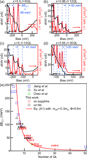
with the effective mass of the bulk valence band which is approximated to be parabolic. We compare our experimental data with this simple model, along with the data for [49, 48] and for [50, 34], as shown in Fig. 5.
For of up to 20 QL, all experimental data follow Eq. 4 with a reasonable effective mass [54, 55] and , when we account for the experimental uncertainty (2 QL) in the estimation of . The significant deviations for films thicker than 25 QL are likely artificial, since the subband splitting is far below the experimentally observed band-edge broadening 30 – 50 meV.
Appendix B Confirmation of rigid-band shift
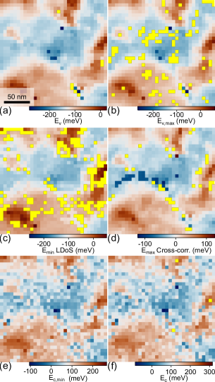
Within the assumption of a rigid-band shift, one expects . Hence, we ensured consistency of our procedure to calculate by determining , , the variations of the minimum in the LDoS (which is the approximate ) and the maximum in the cross-correlation between each spectrum and the average spectrum. Additionally, for computational convenience, we defined onset energies of the bulk valence band () and the bulk conduction band (). As an example, we show the maps of all calculated quantities in Fig. 6 highlighting that the spatial distribution is indeed the same for all of them. To mitigate isolated failures of the numerical determinations, we average over all maps of the six quantities mentioned above to compute the in this paper.
Appendix C Analysis of the Landau level spectra
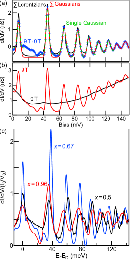
We characterized the width of the Landau levels shown in Fig. 3 and in supplement with the following procedure: First, the spectrum taken at 0 T is subtracted from the spectra in applied magnetic fields, to account for the background. Next, we fit the vicinity (typically 10 meV) of each Landau-level peak with a single Gaussian function to extract the full width at half maximum (FWHM). We find that differences in fitting all Landau levels with a sum of many Gaussians are negligible, and hence used the single peak fitting for computational simplicity for all FWHM values given in the paper.
Interestingly, the line-shape of the Landau levels is found to be more Gaussian than the frequently used Lorentzian [34, 35, 36]. The details of the Landau level line-shape are a subtle issue due to instrumentation factors, but theoretically, a Gaussian line-shape with is expected for quantum smearing from drift motion [45]. Examples of the background subtraction and fitting are shown in Fig. 7.
Appendix D Defect density
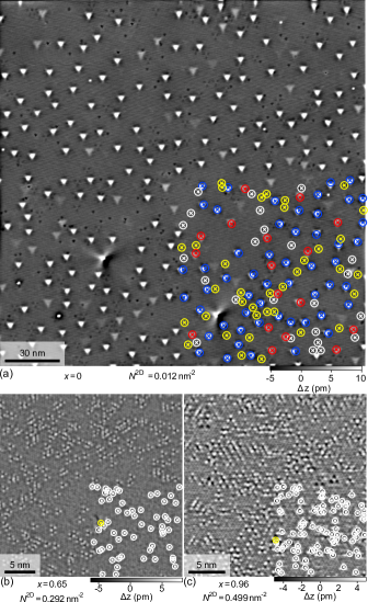
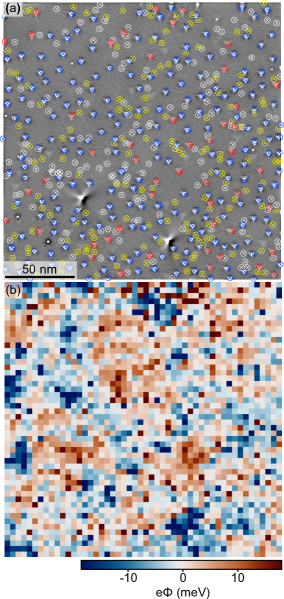
It is well established [41, 56] that STM can directly image the native defects near the surface, i.e. in the top quintuple layer, of TIs. Counting the defects in the three typical STM images shown in Fig. 8 gives the 2D defect densities () indicated in the caption. The defect densities , , and \qty5e20\per\cubic given in Table I are calculated as = /1 nm for the = 0, 0.65, and 0.96 films.
Appendix E Comparison of defect distributions and potential fluctuation
Figure 9 shows a direct comparison of the defect distribution map and the potential map for the same field of view. One can see that there is no apparent correlation between them. This is understandable because the formation of charge puddles is dictated by a long-range statistical distribution of the charged acceptors and donors [12, 28] and there is no reason that the short-range spatial distribution of the charged acceptors/donors has a clear correlation with the local potential. Note also that STM is only sensitive to the charged acceptors/donors near the surface, but the charge puddles will be dictated by the distribution of charges in the whole thickness.
References
- Fu and Kane [2008] L. Fu and C. L. Kane, Superconducting proximity effect and Majorana fermions at the surface of a topological insulator, Phys. Rev. Lett. 100, 096407 (2008).
- Cook and Franz [2011] A. Cook and M. Franz, Majorana fermions in a topological-insulator nanowire proximity-coupled to an -wave superconductor, Phys. Rev. B 84, 201105 (2011).
- Beidenkopf et al. [2011] H. Beidenkopf, P. Roushan, J. Seo, L. Gorman, I. Drozdov, Y. S. Hor, R. J. Cava, and A. Yazdani, Spatial fluctuations of helical Dirac fermions on the surface of topological insulators, Nature Physics 7, 939 (2011).
- Chong et al. [2020] Y. X. Chong, X. Liu, R. Sharma, A. Kostin, G. Gu, K. Fujita, J. C. S. Davis, and P. O. Sprau, Severe Dirac mass gap suppression in Sb2Te3-based quantum anomalous hall materials, Nano Letters 20, 8001 (2020).
- Okada et al. [2012] Y. Okada, W. Zhou, C. Dhital, D. Walkup, Y. Ran, Z. Wang, S. D. Wilson, and V. Madhavan, Visualizing Landau levels of Dirac electrons in a one-dimensional potential, Phys. Rev. Lett. 109, 166407 (2012).
- Fu et al. [2013] Y.-S. Fu, T. Hanaguri, S. Yamamoto, K. Igarashi, H. Takagi, and T. Sasagawa, Memory effect in a topological surface state of Bi2Te2Se, ACS Nano 7, 4105 (2013).
- Lee et al. [2015] I. Lee, C. K. Kim, J. Lee, S. J. L. Billinge, R. Zhong, J. A. Schneeloch, T. Liu, T. Valla, J. M. Tranquada, G. Gu, and J. C. S. Davis, Imaging Dirac-mass disorder from magnetic dopant atoms in the ferromagnetic topological insulator Cr(Bi0.1SbTe3, Proc. Nat. Acad. Sci. 112, 1316 (2015).
- Pauly et al. [2015] C. Pauly, C. Saunus, M. Liebmann, and M. Morgenstern, Spatially resolved Landau level spectroscopy of the topological Dirac cone of bulk-type : Potential fluctuations and quasiparticle lifetime, Phys. Rev. B 92, 085140 (2015).
- Fu et al. [2016] Y.-S. Fu, T. Hanaguri, K. Igarashi, M. Kawamura, M. S. Bahramy, and T. Sasagawa, Observation of Zeeman effect in topological surface state with distinct material dependence, Nature Communications 7, 10829 (2016).
- Storz et al. [2016] O. Storz, A. Cortijo, S. Wilfert, K. A. Kokh, O. E. Tereshchenko, M. A. H. Vozmediano, M. Bode, F. Guinea, and P. Sessi, Mapping the effect of defect-induced strain disorder on the Dirac states of topological insulators, Phys. Rev. B 94, 121301 (2016).
- Knispel et al. [2017] T. Knispel, W. Jolie, N. Borgwardt, J. Lux, Z. Wang, Y. Ando, A. Rosch, T. Michely, and M. Grüninger, Charge puddles in the bulk and on the surface of the topological insulator studied by scanning tunneling microscopy and optical spectroscopy, Phys. Rev. B 96, 195135 (2017).
- Skinner et al. [2013] B. Skinner, T. Chen, and B. I. Shklovskii, Effects of bulk charged impurities on the bulk and surface transport in three-dimensional topological insulators, Journal of Experimental and Theoretical Physics 117, 579 (2013).
- Huang and Shklovskii [2021a] Y. Huang and B. I. Shklovskii, Disorder effects in topological insulator nanowires, Phys. Rev. B 104, 054205 (2021a).
- Dartiailh et al. [2020] M. C. Dartiailh, S. Hartinger, A. Gourmelon, K. Bendias, H. Bartolomei, H. Kamata, J.-M. Berroir, G. Fève, B. Plaçais, L. Lunczer, R. Schlereth, H. Buhmann, L. W. Molenkamp, and E. Bocquillon, Dynamical separation of bulk and edge transport in HgTe-based 2D topological insulators, Phys. Rev. Lett. 124, 076802 (2020).
- Gourmelon et al. [2023] A. Gourmelon, E. Frigerio, H. Kamata, L. Lunczer, A. Denis, P. Morfin, M. Rosticher, J.-M. Berroir, G. Fève, B. Plaçais, H. Buhmann, L. W. Molenkamp, and E. Bocquillon, Velocity and confinement of edge plasmons in HgTe-based two-dimensional topological insulators, Phys. Rev. B 108, 035405 (2023).
- Kamata et al. [2022] H. Kamata, H. Irie, N. Kumada, and K. Muraki, Time-resolved measurement of ambipolar edge magnetoplasmon transport in InAs/InGaSb composite quantum wells, Phys. Rev. Res. 4, 033214 (2022).
- Röper et al. [2024] T. Röper, H. Thomas, D. Rosenbach, A. Uday, G. Lippertz, A. Denis, P. Morfin, A. A. Taskin, Y. Ando, and E. Bocquillon, Propagation, dissipation and breakdown in quantum anomalous hall edge states probed by microwave edge plasmons (2024), arXiv:2405.19983 [cond-mat.mes-hall] .
- Shamim et al. [2022] S. Shamim, P. Shekhar, W. Beugeling, J. Böttcher, A. Budewitz, J.-B. Mayer, L. Lunczer, E. M. Hankiewicz, H. Buhmann, and L. W. Molenkamp, Counterpropagating topological and quantum Hall edge channels, Nature Communications 13, 2682 (2022).
- Zhou et al. [2023] L.-J. Zhou, R. Mei, Y.-F. Zhao, R. Zhang, D. Zhuo, Z.-J. Yan, W. Yuan, M. Kayyalha, M. H. W. Chan, C.-X. Liu, and C.-Z. Chang, Confinement-induced chiral edge channel interaction in quantum anomalous Hall insulators, Phys. Rev. Lett. 130, 086201 (2023).
- Lippertz et al. [2022] G. Lippertz, A. Bliesener, A. Uday, L. M. C. Pereira, A. A. Taskin, and Y. Ando, Current-induced breakdown of the quantum anomalous Hall effect, Phys. Rev. B 106, 045419 (2022).
- Parra et al. [2017] C. Parra, T. H. Rodrigues da Cunha, A. W. Contryman, D. Kong, F. Montero-Silva, P. H. Rezende Gonçalves, D. D. Dos Reis, P. Giraldo-Gallo, R. Segura, F. Olivares, F. Niestemski, Y. Cui, R. Magalhaes-Paniago, and H. C. Manoharan, Phase separation of Dirac electrons in topological insulators at the spatial limit, Nano Lett. 17, 97 (2017).
- Scipioni et al. [2018] K. L. Scipioni, Z. Wang, Y. Maximenko, F. Katmis, C. Steiner, and V. Madhavan, Role of defects in the carrier-tunable topological-insulator () thin films, Phys. Rev. B 97, 125150 (2018).
- Flötotto et al. [2018] D. Flötotto, Y. Ota, Y. Bai, C. Zhang, K. Okazaki, A. Tsuzuki, T. Hashimoto, J. N. Eckstein, S. Shin, and T.-C. Chiang, Superconducting pairing of topological surface states in bismuth selenide films on niobium, Sci. Adv. 4, eaar7214 (2018).
- Yang et al. [2014] F. Yang, A. A. Taskin, S. Sasaki, K. Segawa, Y. Ohno, K. Matsumoto, and Y. Ando, Top gating of epitaxial (Bi1-xSbx)2Te3 topological insulator thin films, Appl. Phys. Lett. 104, 161614 (2014).
- Taskin et al. [2017] A. A. Taskin, H. F. Legg, F. Yang, S. Sasaki, Y. Kanai, K. Matsumoto, A. Rosch, and Y. Ando, Planar hall effect from the surface of topological insulators, Nat. Communun. 8, 1340 (2017).
- [26] See Supplemental Information for additional data and discussions.
- Morgenstern et al. [2003] M. Morgenstern, J. Klijn, C. Meyer, and R. Wiesendanger, Real-space observation of drift states in a two-dimensional electron system at high magnetic fields, Phys. Rev. Lett. 90, 056804 (2003).
- Skinner and Shklovskii [2013] B. Skinner and B. I. Shklovskii, Theory of the random potential and conductivity at the surface of a topological insulator, Phys. Rev. B 87, 075454 (2013).
- Huang and Shklovskii [2021b] Y. Huang and B. I. Shklovskii, Disorder effects in topological insulator thin films, Phys. Rev. B 103, 165409 (2021b).
- Bömerich et al. [2017] T. Bömerich, J. Lux, Q. T. Feng, and A. Rosch, Length scale of puddle formation in compensation-doped semiconductors and topological insulators, Phys. Rev. B 96, 075204 (2017).
- Fu et al. [2014] Y.-S. Fu, M. Kawamura, K. Igarashi, H. Takagi, T. Hanaguri, and T. Sasagawa, Imaging the two-component nature of Dirac-Landau levels in the topological surface state of Bi2Se3, Nature Physics 10, 815 (2014).
- Hashimoto et al. [2008] K. Hashimoto, C. Sohrmann, J. Wiebe, T. Inaoka, F. Meier, Y. Hirayama, R. A. Römer, R. Wiesendanger, and M. Morgenstern, Quantum hall transition in real space: From localized to extended states, Phys. Rev. Lett. 101, 256802 (2008).
- Cheng et al. [2010] P. Cheng, C. Song, T. Zhang, Y. Zhang, Y. Wang, J.-F. Jia, J. Wang, Y. Wang, B.-F. Zhu, X. Chen, X. Ma, K. He, L. Wang, X. Dai, Z. Fang, X. Xie, X.-L. Qi, C.-X. Liu, S.-C. Zhang, and Q.-K. Xue, Landau quantization of topological surface states in , Phys. Rev. Lett. 105, 076801 (2010).
- Jiang et al. [2012a] Y. Jiang, Y. Wang, M. Chen, Z. Li, C. Song, K. He, L. Wang, X. Chen, X. Ma, and Q.-K. Xue, Landau quantization and the thickness limit of topological insulator thin films of , Phys. Rev. Lett. 108, 016401 (2012a).
- Hanaguri et al. [2010] T. Hanaguri, K. Igarashi, M. Kawamura, H. Takagi, and T. Sasagawa, Momentum-resolved Landau-level spectroscopy of Dirac surface state in , Phys. Rev. B 82, 081305 (2010).
- Storz et al. [2018] O. Storz, P. Sessi, S. Wilfert, C. Dirker, T. Bathon, K. Kokh, O. Tereshchenko, and M. Bode, Landau level broadening in the three-dimensional topological insulator , phys. status solidi (RRL) 12, 1800112 (2018).
- Bagchi et al. [2022] M. Bagchi, J. Brede, and Y. Ando, Observability of superconductivity in Sr-doped at the surface using scanning tunneling microscope, Phys. Rev. Mater. 6, 034201 (2022).
- Hernangómez-Pérez et al. [2013] D. Hernangómez-Pérez, J. Ulrich, S. Florens, and T. Champel, Spectral properties and local density of states of disordered quantum hall systems with Rashba spin-orbit coupling, Phys. Rev. B 88, 245433 (2013).
- Zhang et al. [2011] J. Zhang, C.-Z. Chang, Z. Zhang, J. Wen, X. Feng, K. Li, M. Liu, K. He, L. Wang, X. Chen, Q.-K. Xue, X. Ma, and Y. Wang, Band structure engineering in (BiSbTe3 ternary topological insulators, Nature Communications 2, 574 (2011).
- Frantzeskakis et al. [2017] E. Frantzeskakis, S. V. Ramankutty, N. de Jong, Y. K. Huang, Y. Pan, A. Tytarenko, M. Radovic, N. C. Plumb, M. Shi, A. Varykhalov, A. de Visser, E. van Heumen, and M. S. Golden, Trigger of the ubiquitous surface band bending in 3d topological insulators, Phys. Rev. X 7, 041041 (2017).
- Dai et al. [2016] J. Dai, D. West, X. Wang, Y. Wang, D. Kwok, S.-W. Cheong, S. B. Zhang, and W. Wu, Toward the intrinsic limit of the topological insulator , Phys. Rev. Lett. 117, 106401 (2016).
- Chong [2020] Y. X. Chong, Visualizing quantum anomalous hall states at the atomic scale with STM Landau level spectroscopy, PhD thesis, Cornell University (2020).
- Heffels et al. [2023] D. Heffels, D. Burke, M. R. Connolly, P. Schüffelgen, D. Grützmacher, and K. Moors, Robust and fragile Majorana bound states in proximitized topological insulator nanoribbons, Nanomaterials 13, 10.3390/nano13040723 (2023).
- Münning et al. [2021] F. Münning, O. Breunig, H. F. Legg, S. Roitsch, D. Fan, M. Rößler, A. Rosch, and Y. Ando, Quantum confinement of the Dirac surface states in topological-insulator nanowires, Nature Communications 12, 1038 (2021).
- Champel and Florens [2009] T. Champel and S. Florens, Local density of states in disordered two-dimensional electron gases at high magnetic field, Phys. Rev. B 80, 161311 (2009).
- Breunig and Ando [2022] O. Breunig and Y. Ando, Opportunities in topological insulator devices, Nat. Rev. Phys. 4, 184 (2022).
- Dang et al. [2023] L. T. Dang, O. Breunig, Z. Wang, H. F. Legg, and Y. Ando, Topological-insulator spin transistor, Phys, Rev, Appl, 20, 024065 (2023).
- Chen et al. [2012] M. Chen, J.-P. Peng, H.-M. Zhang, L.-L. Wang, K. He, X.-C. Ma, and Q.-K. Xue, Molecular beam epitaxy of bilayer Bi(111) films on topological insulator Bi2Te3: A scanning tunneling microscopy study, Appl. Phys. Lett. 101, 081603 (2012).
- Xu et al. [2015] J.-P. Xu, M.-X. Wang, Z. L. Liu, J.-F. Ge, X. Yang, C. Liu, Z. A. Xu, D. Guan, C. L. Gao, D. Qian, Y. Liu, Q.-H. Wang, F.-C. Zhang, Q.-K. Xue, and J.-F. Jia, Experimental detection of a Majorana mode in the core of a magnetic vortex inside a topological insulator-superconductor heterostructure, Phys. Rev. Lett. 114, 017001 (2015).
- Jiang et al. [2012b] Y. Jiang, Y. Y. Sun, M. Chen, Y. Wang, Z. Li, C. Song, K. He, L. Wang, X. Chen, Q.-K. Xue, X. Ma, and S. B. Zhang, Fermi-level tuning of epitaxial thin films on graphene by regulating intrinsic defects and substrate transfer doping, Phys. Rev. Lett. 108, 066809 (2012b).
- Yang et al. [2009] M. C. Yang, C. L. Lin, W. B. Su, S. P. Lin, S. M. Lu, H. Y. Lin, C. S. Chang, W. K. Hsu, and T. T. Tsong, Phase contribution of image potential on empty quantum well states in Pb islands on the Cu(111) surface, Phys. Rev. Lett. 102, 196102 (2009).
- Becker and Berndt [2010] M. Becker and R. Berndt, Scattering and lifetime broadening of quantum well states in Pb films on Ag(111), Phys. Rev. B 81, 205438 (2010).
- Chen et al. [2021] G.-Y. Chen, C.-H. Hsu, B.-Y. Liu, L.-W. Chang, D.-S. Lin, F.-C. Chuang, and P.-J. Hsu, Quantum well electronic states in spatially decoupled 2D Pb nanoislands on Nb-doped SrTiO3(001), Applied Surface Science 537, 147967 (2021).
- Köhler [1976] H. Köhler, Non-parabolicity of the highest valence band of Bi2Te3 from Shubnikov-de Haas effect, phys. status solidi (b) 74, 591 (1976).
- von Middendorff et al. [1973] A. von Middendorff, K. Dietrich, and G. Landwehr, Shubnikov-de Haas effect in p-type Sb2Te3, Solid State Communications 13, 443 (1973).
- Lin et al. [2021] Y.-R. Lin, M. Bagchi, S. Soubatch, T.-L. Lee, J. Brede, F. m. c. C. Bocquet, C. Kumpf, Y. Ando, and F. S. Tautz, Vertical position of Sr dopants in the superconductor, Phys. Rev. B 104, 054506 (2021).