Acronyms
Understanding the chemical and structural variability in the efficiency of band edge optical transitions of 2D monolayer materials
Abstract
We conducted a high-throughput density functional theory calculation and comprehensive analysis of the momentum matrix elements between the band edges across a wide range of nonmagnetic two-dimensional monolayer materials with direct band gaps. The primary objectives of our study were twofold: (i) to identify and rank the materials as potential optical emitters and (ii) to enhance our understanding of the physical and chemical factors that determine the strength of the optical coupling. From the studied ensemble of materials, a significant number of them presented allowed optical transitions between the valence band edge and the conduction band edge. In these cases, the momentum matrix elements range from nearly 0 to 1.13 at.u., depending on the specific structure and composition of the materials. By comparison, the most prominent group III-V bulk semiconductors have momentum matrix elements on the order of 1 at.u., indicating the high potential of two-dimensional monolayer materials as optical emitters. We considered different types of materials based on their elemental composition and applied a criterion derived from the atomic orbital selection rules for electronic transitions. In the case of materials composed solely of elements from the p-block of the periodic table, as well as materials with transitions at the high-symmetry point in the Brillouin zone, we obtained highly predictable results. However, for materials that were not explained by the criterion, we observed the occurrence of the direct band gap at a -point different from and the absence of centrosymmetry in their space groups. Finally, we examined the prominent family of monolayer transition metal dichalcogenides, which exhibited high optical coupling and low criterion values. We propose a connection between the significant contribution to the momentum matrix elements for interband optical transitions and the anomalous Born effective charge phenomena. The implications of this phenomenon are such that, unlike materials that exhibit conventional Born effective charges, in which increased ionicity leads to diminished optical coupling. If the anomalous situation is present, it arises from a distinctive charge transfer and bonding mechanism, resulting in a positive correlation between ionicity and the optical coupling.
I Introduction
The emergence of two-dimensional monolayer materials (2DMs) as physically realizable systems has resulted in one of the most active fields in modern materials research [1, 2, 3]. Atomically thin materials provide an ideal platform for investigating electronic physical properties under quantum confinement, particularly, the enhancement of excitonic effects [1, 2, 3]. Reducing layered materials to a single sheet opens up possibilities for modifying the optoelectronic properties of materials, such as band gap engineering [4]. Furthermore, the transition from a bulk material to a two-dimensional monolayer material can lead to a crossover from an electronic indirect band gap to a direct band gap material, which is promising for light-emitting applications. Prominent examples of materials that exhibit this band character modification include members of the transition metal dichalcogenides (TMDC) family [5, 6], tellurene [7], and phosphorene (black phosphorus) [8, 9, 10]. Among the TMDC family, the monolayer of molybdenum disulfide \ceMoS2 has been extensively studied, and its electronic properties have been predicted through ab initio simulations and confirmed by experiments [5, 11, 12]. This 2D direct band gap semiconductor material exhibits strong light emission though luminescence [13, 14], high light absorption [15], strongly bound exciton peaks [5], and circular dichroism [16, 17]. As a result, there is a growing interest in studying the optical properties of 2D direct-band gap materials [18, 19, 20, 21, 22, 23, 24].
The squared magnitude of the matrix element , characterizes the strength of the optical coupling between an initial quantum state to a final state via photon absorption, where corresponds to the light perturbation Hamiltonian. In the case of crystalline material, assuming the electron dipole approximation, the inter-band optical matrix elements for unpolarized light are directly proportional to the momentum matrix elements, denoted as . Here, represents the momentum operator, represents a point in the Brillouin zone (BZ) and () represents a Bloch state in the occupied valence (empty conduction) band (see Refs. [25, chap. 3], and [26, chap. 9]). These matrix elements are used as input parameters in the method of electronic bandstructure calculation [27, chap. 2.6]. For instance, they have been employed to construct a model that describes the dispersion at the band extrema for 2D monolayer TMDCs (\ce2 with : Mo and W, and : S, Se and Te) [28]. The momentum matrix elements play a crucial role in studying the absorption and emission properties of direct band gap semiconductors [29, 30, 31], as they are a key factor for the calculation of the optical absorption coefficient, and luminescence intensity [25, chap. 3 and 4]. For bulk group-IV, III-V, and II-VI semiconductors, the momentum matrix elements expressed in energy units ( [27, p. 71], where is the rest mass of an electron) have been evaluated in the range of 1431.4 eV [32, 33, 34, 35]. These traditional optoelectronic materials matrix elements display low sensitivity to the chemical composition variability.
The rationalization of the strength of dipole optical transitions can be divided into two main categories. The first category involves the use of group theory as a mathematical framework (see [36, chap. 6.6] and [37, chap. 10]). Lynch [37] emphasizes the usefulness of group theory in identifying cases where dipole matrix elements become zero, providing a tool for establishing selection rules. Group theory has been applied to investigate dipole transitions in bulk halide double perovskites [38], study the phosphorene monolayer [39], and verify selection rules through experimental photoluminescence measurements in monolayers of TMDCs (\ceWSe2, \ceWS2, and \ceMoSe2) [40]. However, no estimation of the oscillator strength could be performed in the latter case. In materials with inversion symmetry, optical dipole transitions only occur between bands with opposite parity. This consideration of parity has been applied in lead-free metal halide and double perovskites [41]. Furthermore, the inference of band parity based on the orbital contribution was utilized to explain experimental photoluminescence measurements in double perovskites [42]. For materials without inversion symmetry, the symmetry of the entire electronic states must be taken into account. The matrix element vanishes only if is orthogonal to all the basis functions of the decomposition of into irreducible representations [36, chap. 6.6]. Nevertheless, group theory alone is insufficient for the comprehensive analysis of allowed optical transitions, as it does not provide a methodology for determining the magnitude of band coupling.
The second category involves an analysis of various material properties derived from the electronic structure to rationalize the strength of dipole optical transitions. The band-edge light absorption in hybrid perovskite solar cell materials has been examined through density functional theory (DFT) calculations of the band-edge oscillator strength [43], given by [25, app. B]. This analysis was conducted at the direct band-gap k-point, where represents the energy difference between states in the conduction and valence bands involved in the transition, and is the position operator. The conclusion from the study was that an increase in can be attributed to the greater overlap between the valence band edge (VBE) and conduction band edge (CBE) states. Alternative studies relied on the quantum mechanical bonding parameters of electrons transferred and electrons shared, calculated using the atoms in molecules theory [44]. Lead chalcogenides (\cePb, with : \ceTe, \ceSe, \ceS, \ceO) were investigated, and a reduction in the band-edge oscillator strength was found with higher electrons transferred due to decreased orbital overlap. It should be noted, that they introduced the average matrix elements as the ratio between the dielectric function and the joint density of states, which is proportional to . In the case of halide perovskites [45, 46], a decrease in was linked to reduced overlap based on increased electrons shared and electrons transferred. Likewise, for monochalcogenides (, with : Pb, Sn, Ge and : Te, Se, S; excluding \ceGeS) [47], a decrease in was associated with reduced orbital overlap, as suggested by a decrease in the maximum photon absorption due to increased electrons transferred and electrons shared. Moreover, the optical absorption of halide perovskites (\ceCsPb3 with : I, Br, Cl; and \ceCsSnI3) above the band-gap was studied through the computation of the dipole matrix elements , and noted an inverse relationship between dipole matrix elements and the electronic bandgap value [48]. Finally, the band-edge oscillator strength of phosphorene was analyzed via DFT calculations [49]. The projected orbital character of the Kohn-Sham functions and their correspondence with the dipole selection rules for atomic orbitals was examined, but no numerical criterion or predictor was established.
It is noteworthy that both the oscillator strength and the dipole matrix elements are influenced by the band gap value. This influence arises from the relationship . However, accurately determining the band gap in standard DFT calculations can be problematic, making it challenging to compare optical coupling at the band edge between different materials. On the other hand, is not affected by the band gap error, providing a more suitable metric for comparing materials [50],[51, app. A]. Although these different approaches offer various perspectives on the strength of interband optical transitions in semiconductor crystalline materials, there is no general methodology for analyzing the optical coupling at the band edge. As such, currently, there is no criterion that serves as a good predictor for the wide variability of the values in 2DMs, as will be demonstrated in the following sections. Considering the promising optoelectronic applications of 2DMs, we anticipate that gaining insight into the band-edge optical transitions could improve our understanding of the coupling variability in these materials and aid in ranking them accordingly.
Our study focused on investigating the momentum matrix elements of 2DMs using DFT [52, 53] in a high-throughput manner. The structures used in our study were obtained from the Computational 2D Materials Database [54, 55], and the band-gaps reported in the database were verified through our DFT calculations. Specifically, we focused on nonmagnetic semiconductors with a direct electronic band gap of up to 3.5 eV. Out of the total 15,733 materials in the database, after filtering according to the parameters explained in Sec. II, we calculated the momentum matrix elements between the VBE and CBE, for 358 monolayers. To analyze the data, we initially tested previously proposed predictors for the optical coupling at the band edge, such as the orbital similarity [56] and the spatial overlap between the electronic wavefunctions [57]. Unfortunately, we found that these approaches lack predictability when applied to our ensemble of 2DMs. Therefore, we propose a quantifiable criterion that relates to the orbital character of the Kohn-Sham wave functions corresponding to the edges of the valence and conduction bands. We initially tested this criterion on the ensemble of 2DMs and verified its correlation with the momentum matrix elements. The criterion is based on the selection rules for orbital transitions, which govern the coupling of atomic orbitals through the electric dipole operator. Our approach builds upon the work of Tran et al. [49], who initially applied the idea to the phosphorene monolayer, and we develop it into a comprehensive numerical methodology that can be applied to a wide range of materials. We ensured that the criterion captured the intensive nature of the physical property under study. Furthermore, for special cases falling outside the applicability of the criterion, we elucidated the physical properties presented and their effects on the optical coupling between the VBE and CBE. We propose a connection between the significant contribution to the momentum matrix elements of TMDCs and the presence of a bond originating from the charge transfer from the chalcogen to the transition metal (TM) atom, as originally noted by Pike et al. [58] to elucidate the anomalous Born effective charge (BEC) behavior. Finally, we highlight the comparable strength of the optical coupling at the band edges obtained for the 2DMs with those of traditional optoelectronic bulk semiconductors.
II Computational details
The crystal structures utilized in this investigation were obtained from the C2DB database [54], and were selected based on their dynamic and thermodynamic stability. This selection criterion required nonimaginary frequencies in the phonon dispersion and energy values above the convex hull of less than 50 meV per atom. The DFT [59, 60] based calculations were conducted using the vasp package [61, 62] (version 6.4.0), which employs the projector augmented wave pseudopotential method for the basis set treatment [63]. The Perdew–Burke-Ernzerhof (PBE) exchange-correlation functional was employed [64]. The selected cutoff energy for the plane wave expansion was set to the maximum ENMAX parameter (POTCAR file) from the atomic species in the compounds. For the pseudo-potentials approximation, the version 5.4 of the POTCAR files were employed and the number of valence electrons and cutoff energy for each pseudo-potential can be found in Table S1 from the Supplementary Material (SM) [65]. A -centered unshifted -mesh was utilized. For this purpose, we employed the fully automatic generation scheme with a parameter, which determines the number of subdivisions for every lattice vector as . In cases where the -point for the band edges was not included in the automatic mesh, it was explicitly added to the list with a weight of zero for the computation of the momentum matrix elements. The precision mode employed with the PREC flag was accurate, this defines the fast Fourier transform grid NG(X,Y,Z), where NG represents the number of points along the lattice vector. With the selected mode, , where . \AcSOC was considered in all calculations [66]. The convergence criteria for the total energy in the electronic self-consistent field loop was set at eV. For the orbital partial occupancies, we used a 0.01 eV Gaussian smearing width. The momentum matrix elements were transformed from the dipole matrix elements (WAVEDER file), as . Convergence tests for the squared momentum matrix elements, were performed for three representative materials of the ensemble with respect to the , cutoff energy and precision mode computational parameters, and are presented in Fig. S1 of the SM [65].
III Results and discussion
III.1 Momentum matrix elements:
As a first step, we have computed the momentum matrix elements, denoted as , between the valence and conduction band edges based on the electronic band structure of 2DMs. These matrix elements are essential for understanding optical emission due to the recombination of charge carriers between CBE and VBE. Our study specifically focuses on direct band gap 2DMs. In general, band degeneracies may arise at the band edges. In the presence of such degeneracies, we consider all possible transitions between the groups of bands that conform the CBE and VBE as follows:
| (1) |
for instance, in monolayer \ceReS2 the direct transition is located at the high-symmetry point in the BZ. The VBE and CBE consist of degenerate bands and , respectively. In other cases, degeneracies are lifted due to symmetry conditions or by spin-orbit coupling (SOC), as seen in monolayer \ceMoS2. For our analysis, bands are considered as part of CBE or VBE if their eigenvalues differ by less than 0.25 eV. The justification for this threshold will be discussed later when examining the significance of excitonic effects. Additionally, we take into account the symmetry multiplicity of in the irreducible-BZ, which depends on the specific space group of each material. Lastly, the index specifies the Cartesian direction.
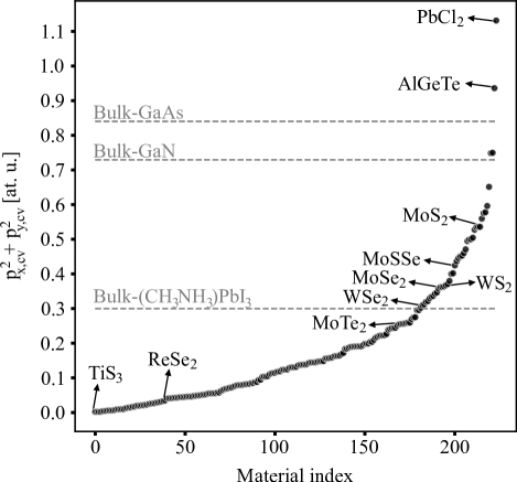
The computed results for the square of the in-plane momentum matrix elements for all the materials filtered from the C2DB database using the selection criteria outlined in Sec. II are presented in Fig. 1. Here, the out-of-plane is left aside as it is generally negligible for 2DMs. Interestingly, several materials are highlighted on this plot: \cePbCl2 and \ceAlGeTe because, according to our calculations, those exhibit the highest optical coupling between CBE and VBE, although they have not been reported experimentally. Also in Fig. 1 are shown the compounds \ceMoS2 [11, 12, 68, 69, 5, 13, 14, 16, 17, 15, 70, 71], \ceMoSSe [69], \ceMoSe2 and \ceWSe2[68], \ceMoTe2 [72], \ceReSe2 [73], \ceWS2[74] and \ceTiS3[75] as prominent 2DMs that have been successfully synthesized. In some cases, not labeled in Fig. 1, such as \ceInTe, where \ce: \ceBr, \ceI, with at.u and at.u, respectively; and \ceTeO2, with at.u, a bulk layered phase exists in nature, which makes exfoliation of a monolayer plausible. The gray dashed lines in Fig. 1 represent the values for selected bulk semiconductors computed at the same level of theory, i.e., DFT-PBE [67] capturing transitions between the CBE and VBE. The 0.25 eV eigenstates energy window was also employed, for an equitable comparison of the optical coupling with the 2DMs. This selection excludes the split-off band in \ceGaAs and includes the heavy hole, light hole, and split-off band at the k-point for \ceGaN, and the doubly degenerate valence and conduction band edge at the k-point for \ce(CH3NH3)PbI3. Based on this comparison, the best 2DMs have comparable optical coupling to established bulk optoelectronic materials.
To validate the calculated momentum matrix elements obtained within the DFT-PBE framework, we compare the computed values with results from bulk materials employing DFT with hybrid exchange-correlation functionals and experimentally inferred results. It should be noted that, for the hybrid and experimental cases reported in the literature, the calculation of the optical coupling corresponds to considering only one conduction band eigenstate, , and includes the contribution from the heavy hole, light hole, and split-off band, , given by:
| (2) |
This energy expression, , is inherited from the effective mass of conduction band electrons , which is given in terms of [in contrast to Eq. (1)] by the k p perturbation theory applied at the band edge (see Ref.[76, 77] and [27, p. 71]). In order to benchmark our results for the momentum matrix elements, we selected well-studied materials: bulk GaAs, GaN, and monolayer \ceMoS2. For bulk wurzite-\ceGaN, our [Eq. (2)] value is 0.36 at.u. (PBE), 0.49 at.u [78, 67] from both Heyd–Scuseria–Ernzerhof (HSE06) [79, 80] and Yukawa screened hybrid (YSH) [81] hybrid functionals, and the experimental values range from 0.51 to 0.69 at.u. [30, 82, 35]. For bulk-\ceGaAs, our value is 0.62 at.u. (PBE), 0.80 at.u. [67] from both HSE06 and YSH hybrid functionals, and the experimental values range from 0.83 to 1.1 at.u. [83, 33, 32, 34, 35]. Finally, for the 2D-\ceMoS2 monolayer, our value is 0.14 at.u. (PBE) and 0.21 at.u. [67] from the YSH exchange-correlation functional. It is worth noting that in the case of nonlocal potentials, such as hybrid functionals, the velocity matrix elements , where is the imaginary unit, need to be evaluated. However, for local potentials, these are equivalent to the momentum matrix elements [84, 85, 86, 67]. Although DFT-PBE underestimates the strength of the optical coupling by approximately 35%, the observed error is systematic, which lead us to expect that trends in the efficiency of optical transitions at the band edges between materials, as inferred from DFT-PBE, remain valid.
The results presented in this study are based on the independent particle approximation provided by DFT and can be considered as an initial approach for studying the excitation properties of 2DMs. It has been established that higher-level theories are required to accurately describe excitonic effects and electronic screening [87, chap. 20], [88, chap. 21], [89]. However, due to the high-throughput nature of this study, solving the Bethe–Salpeter equation (BSE) equation for all the materials studied is not feasible. Moreover, the BSE level still relies on DFT for the calculation of the exciton envelope function which comprises of the single-particle wave functions, considering bands and wave vectors in the vicinity of the band edges [90] (see Ref. [26, chap. 9.5]). As well as for the calculation of the exciton oscillator strength, obtained by weighting the matrix elements by the envelope function coefficients. On the other hand, excitonic effects lead to an additional enhancement of the optical coupling between states near the band edges, and a reduction of oscillator strengths at higher energies compared to results inferred from the independent particle approximation [87, chap. 20.2 and 20.3], [91]. We use an energy range selection of 0.25 eV to account for the enhancement of optical coupling strength associated with the inclusion of excitonic effects. This tolerance is chosen by considering half of the average of the reported exciton binding energies for the ensemble of 2DMs.
III.2 Rationalizing variability of momentum matrix elements:
To elucidate the underlying chemical trend responsible for the observed optical coupling variability depicted in Fig. 1, it is advantageous to conduct an analysis of the Kohn-Sham states obtained from the DFT calculations. The aim is to identify useful parameters or descriptors derived from the characteristics of electronic states relevant to optical transitions at the band edges.
III.2.1 Pre-existing knowledge
The first descriptor tested was the IPR [92, 93], which quantifies the localization of states at a band edge with energy eigenvalue . The discrete form of the IPR [94] is given by
| (3) |
where represents the probability of finding an electron in the vicinity of an atomic site . The IPR values range from (fully delocalized) to 1 (fully localized), here is the number of atoms in the computational model. In Ref. 56, the threshold value of 0.35 was selected to differentiate between delocalized and localized states. Woods-Robinson et al. [56] reached the conclusion that highly localized cases predominantly exhibited forbidden transitions.
For the application of this criterion to our 2DMs dataset, we took into consideration the same groups of the VBE and CBE bands within a 0.25 eV window, which were used for the calculation of (Eq. 1). Within each group, we checked for degenerated bands, using a tolerance of eV. For cases of degenerated bands with identical eigenvalues of , special consideration must be taken to compute the IPR. Therefore, we utilized the following expression:
| (4) |
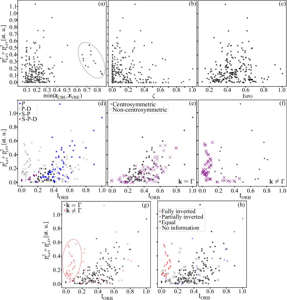
When a band edge included multiple groups of degenerated bands, the total IPR for the band edge was computed as an average of the IPRs from each degenerate group. We applied this criterion to our dataset and present the results in Fig. 2(a), using the minimum value of and as a unique localization predictor of the electronic states at the band edges for a material, here, higher values of indicate a higher level of localization. The materials within the gray oval belong to the family of TMDCs and are the subjects of discussion in Sec. III.3. Contrary to the expected trend proposed in Ref. 56, we do not observe a correlation between materials with low optical coupling () and strong localization (high ). The majority of optically inactive materials display a rather delocalized character of electronic states at the band edges.
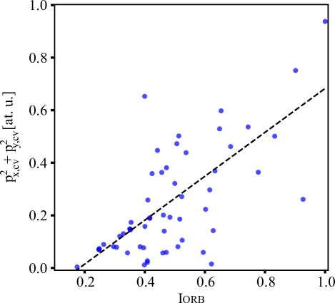
The second descriptor tested was proposed in Ref. 56, and is the orbital similarity between states of the valence band and conduction band given by
| (5) |
Here, represents the orbital character, and () refers to the electron azimuthal (magnetic) quantum number. Optical transitions between states of similar atomic orbitals are expected to have weak optical matrix elements following the optical selection rules. It is important to note that, for our research, the presence of direct allowed transitions is a useful characteristic for designing high-performance light-emitting devices. Consequently, a low orbital similarity is favorable in our case. To apply the orbital similarity criterion to our 2DMs dataset, we employed the same approach for selecting the VBE and CBE groups of bands and the handling of degenerate bands within each group, as was done for the IPR case. Woods-Robinson et al. [56] did not explicitly specify how to obtain the total orbital similarity value for degenerate bands; therefore, we propose the following extension of Eq. (5) for degenerate states
| (6) |
where () is the eigenvalue from the valence (conduction) band at the direct transition -point. Figure 2(b) presents the optical matrix elements as a function of the orbital similarity . In the case of more than one degeneracy in either the VBE or CBE, the angle brackets represent an average over all possible pairs. We found that materials with low orbital similarity between the band edges do not necessarily correspond to high values of .
The third predictor is a simple requirement for optically-induced electronic transitions, the spatial overlap between the electronic wave-functions as proposed by Wełnic et al. [57]. We express the spatial overlap between a group of degenerate valence and conduction states in a discrete form by the equation:
| (7) |
In Figure 2(c) we display the in-plane momentum matrix element for all the 2DMs as a function of the spatial overlap. In the case of multiple degeneracies in either the VBE or CBE, the values represent the average of all possible pairs. Each term in the sum provides a measure of the probability for the electron and hole to be located in the vicinity of the same atomic site . Generally, we observe that the spatial overlap between the VBE and CBE alone is not an effective descriptor for the strength of optical coupling.
III.2.2 Proposed criterion
We propose an alternative numerical criterion, referred to as allowed orbital overlap, for quantifying the optical coupling at the band edge of 2DMs. This criterion is based on the rationale put forth by Tran et al. [49], which utilizes Kohn-Sham states projected onto atomic orbitals within a sphere centered at individual atoms. The allowed orbital overlap is formulated based on the constraint imposed on the optically-induced transitions of electrons between atomic orbitals by the electric dipole selection rules between initial (i) and final (f) states (see Ref. [95, chap. 4.3] and Ref. [96, cpl. ]),
| (8) |
where represents the electron’s azimuthal quantum number. We propose an improvement to the spatial overlap by specifically considering the overlap of allowed orbitals in accordance with Eq. (8). The allowed orbital overlap is defined as
| (9) |
where the terms , and represent the orbital characters of the valence (conduction) band. For each atom , we have a set of orbital characters , and for each energy eigenvalue . To simplify the notation, v (c) refers to either the state with eigenvalue , or in the case of energy degeneracy, the characters are summed for a group of degenerate valence and conduction states. For example, , here are identical eigenvalues. The angle brackets denote an average over all possible pairs within the VBE and CBE. It is worth mentioning that, in this case, spin was not considered for the computational convenience of the criterion. We followed the same approach as in Sec. III.2.1 when selecting the groups of bands for the VBE and CBE, as well as the handling degenerated bands within each group.
Figure 2(d) illustrates the optical matrix elements as a function of . Materials were grouped based on the block in the periodic table of the elements that compose the crystal. No further consideration regarding the bonding or nature of the valence electronic states was employed in this analysis. Materials solely composed of p-block (group 13 to 18) elements (P, 56 structures) exhibit the highest optical coupling strength at the band edge and highest predictability. A linear least-squares regression fitting of and data is presented in Fig.S2 of the SM [65]. For materials containing a mixture of s- (group 1 and 2), p-, and d-block (group 3 to 12) elements (S-P-D, 12 structures), we obtained even a stronger correlation of the data, but they represent small subset of the ensemble and exhibit low values on average (0.1 at.u.). In the case of materials composed of s- and p-block elements (S-P, 31 structures) we found a weak correlation. Finally, for materials composed of d- and p-block elements (P-D, 124 structures), no discernible correlation was observed. Unfortunately, due to the lack of reports, materials composed solely of s-block or d-block elements, as well as those materials comprised of of s- and d-block elements, were not considered. Therefore, the candidates for 2DMs that exhibit the highest allowed optical coupling between the VBE and CBE are those composed solely of p-block elements, such as \cePbCl2 (1.13 at.u.), \ceAlGeTe (0.94 at.u.), \ceInGeSe (0.75 at.u.), \ceInSnTe (0.65 at.u.), and \ceGaClSe (0.60 at.u.). These materials have been computationally predicted and demonstrate significant potential for optoelectronic applications. As previously mentioned, materials such as \ceInBrTe ( at.u.) and \ceInITe ( at.u.) are known to exist in a bulk layered phase in nature, indicating their feasibility for synthesis. The optical coupling values of these latter materials are comparable to those exhibited by experimentally reported materials such as \ceMoS2 (0.54 at.u.), \ceMoSSe (0.45 at.u.), and \ceWS2 (0.40 at.u.). These materials belong to the category containing p- and d-block elements and represent outliers from the criterion trend presented in Figure 2(d), which will be further discussed in the subsequent section.
III.3 Outliers analysis:
In Fig. 2(g), we present the values of the criterion vs , distinguishing between materials with a direct band-gap k-point in the BZ at the high symmetry point and those with k-points different from . We identified 68 materials with transitions not at : 1 from S-P-D, 3 from S-P, 5 from P, and 59 from P-D. On the other hand, 156 materials exhibited transitions at the point: 11 from S-P-D, 28 from S-P, 52 from P, and 65 from P-D. It is notable that most materials with non- k-points contain elements from the d-block of the periodic table. Additionally, the most significant outliers, exhibiting low criterion but high optical coupling (circled in red), from the predictor trend corresponded to non- optical transitions.
From the field of group theory, it is well-known that the point of the BZ of a crystalline structure possesses the highest degree of symmetry since the group of the k-point is equivalent to the full point group of the crystal. In contrast, other high-symmetry points and the paths that connect them within the BZ exhibit either the same or lower symmetry when compared to the point (see Ref. [87, chap. 20.1.3] and Ref. [27, chap. 2.3.4]). When symmetry is reduced, as in the case for non- points, the selection rules governing the optical transitions can be relaxed. Consequently, the applied criterion lacks predictability. This limitation, which obstructs the interpretation of the single-particle optical properties in crystalline materials within the atomic picture, has been pointed out earlier in the context of TM oxides (\ceO, = \ceMn, \ceFe, \ceCo, \ceNi) [97]. In this case, the VBE and CBE were solely composed of contributions from orbitals. The authors concluded that to explain the magnitude of at non- k-points, transitions between atoms at different sites involving to , as octahedral crystal-field levels, must be taken into consideration.
A notable category of materials that deviate from the trend presented in Fig. 2(d) are the TMDCs monolayers. These materials exhibit low values but high values [circled region in Fig. 2(g)]. Moreover, they belong to the category (P-D) of materials with - hybridization and exhibit a direct band gap that occurs away from the point. Materials in this region of the graph, which are not TMDCs, typically contain one or more of the TM elements (\ceMo, \ceCr, \ceW, \ceNb, \ceTa). Another common feature among the materials in this region is that their crystal structures belong to a noncentrosymmetric space group, as shown in Fig. 2(f). It should be noted that for materials with transitions at [Fig. 2(e)], the presence, or absence, of centrosymmetry in the space group does not affect the predictive power of the criterion. It is well established that for inorganic TM complexes, the lack of a center of symmetry leads to the mixing of and orbitals. The mechanism for the mixing is the shared point group representation of the orbitals. The lifting of the selection rules and apparent ’-’ optical transitions, come from the transitions between the - and - characters of the atomic orbitals involved (see Ref. [98, chap. 9.6] and Ref. [99, chap. 11.3.1]).
In TMDCs, such as \ceMoS2, the electronic band-edges are primarily composed of -orbitals of the \ceMo atom, with a small contribution from the -orbitals of sulfur. Specifically, in the valence band at the k-point, Mo: -orbitals, and are present, along with a small contribution from the sulfur orbitals, and . In the conduction band at the k-point, the dominant orbital contribution comes from the Mo orbital [100, 28]. According to atomic selection rules, this orbital composition is not expected to result in significant optical coupling. However, there are multiple proposed explanations for the observed interband optical coupling in this material. The first proposed explanation, is the potential role of SOC in enabling dipole transitions [101, 24]. To further investigate this, we performed additional calculations of \ceMoS2 without considering SOC and found that SOC effect in value is negligible. The second proposed explanation is the trigonal prismatic crystal field splitting of \ceMo- states. This idea was suggested by a previous study on bulk \ceMoS2 [102]. To test this idea, we conducted a DFT calculation using a computational cell containing a single \ceMo atom surrounded by six \ceS atoms, while maintaining the inter-atomic distances from the monolayer. In this case, the stoichiometry is different from \ceMoS2, but this affects only the band occupancy. The results confirmed the crystal field splitting for the -electronic levels of \ceMo, with a lower energy level composed of followed by two degenerate energy levels composed of and , and a twofold degenerate higher energy levels composed of and . However, no optical coupling between and states was observed. From the picture of the atomic orbital selection rules, the only pathway for the inter-band transitions between the VBE and CBE is through the sulfur valence band contribution to the conduction bands of molybdenum, as pointed out by Kumar and Ahluwalia [103].
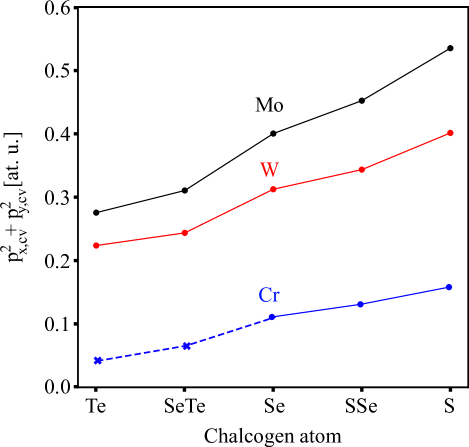
To perform a detailed analysis to the group of outliers [Fig. 2(g), circled in red], we specifically chose \ce2 (space-group no. 187) and \ce (space-group no. 156) TMDCs, with Mo, W, Cr; and (): S, Se, Te. The - distance, which is equal to the lattice parameter for the hexagonal cell, increases with the atomic number of the chalcogen and the atomic radius of the chalcogen. The change in - distance (0.14 Å on average from Te to Se and Se to S) is of a similar magnitude as the increase in chalcogen size (0.175 Å on average). However, the optical coupling values increase significantly as we move up the periodic table for the chalcogen atom, as shown in Fig. 3. To further investigate this phenomenon, we conducted a computational experiment by replacing the sulfur atom with a tellurium atom in the \ceMoS2 structure while keeping the structural parameters unchanged. As the lattice parameter remained constant and the chalcogen selected was larger, we expected to obtain an increased optical coupling strength value, if the enhanced Mo- overlap was the cause. Nevertheless, the obtained optical coupling was only half of the value compared to the \ceMoS2 monolayer case, suggesting the significance of the chemical environment rather than solely the inter-atomic distance.
Additionally, considering the previous group of monolayer TMDCs, in Fig. 3 we evidence a chemical trend between the chalcogen atom(s) with the optical coupling strength. To elucidate the trend, we analyzed the following physical quantities related to the bonding nature of these materials (see Fig. S3 of the SM [65]). Firstly, the well known electronegativity tendency of the chalcogen is correlated with the Bader charges value of the TM atom, and a decrease in BECs magnitude. Considering these interconnected quantities, the increase in charge transfer between the TM atom and the chalcogen suggests a greater ionic character, resulting in enhanced optical coupling. This is in contrast to covalent bonded semiconductors, where increased orbital overlap, and consequently, electron hopping would enhance optical coupling. In this case, however, we observe a correlation with electron charge transfer.
To elucidate the counterintuitive behavior observed, it is crucial to consider that, in the case of the examined TMDCs monolayers, the Bader static and Born dynamic charges exhibit opposite signs [see Fig. S3(c) of the SM [65]]. This phenomenon was explained by Pike et al. [58], where they discovered a significant local change of electronic density around the TM atom due to atomic perturbations, such as electric fields or atomic displacements. This change was attributed to the presence of a localized bond, superposition of Mo , Mo , and S orbital states. The charge transfer mechanism proposed by Pike et al. [58] is the following, ”In the case of \ceMoS2, the Mo atoms share their electrons with the S atoms, which transfer back their electrons to the Mo atoms (antibonding state composed of orbitals) in order to fill the orbital of Mo”. This idea is supported by the positive Bader charge (static picture) of the TM atom indicating depletion of electronic density, which in response to a perturbation exhibits a negative Born effective charge (dynamic picture), evidencing the presence of electronic density around the TM atom. Therefore, the high optical coupling observed in the outliers from the trend presented in Fig. 2(d) can be explained by the the aforementioned local bond from the antibonding orbital localized around the TM, causing the counterintuitive sign of the BECs. This localized bond can be considered as a pseudocovalency, as it involves the character of the -orbitals from the TM and the -orbitals of the chalcogen. The increased optical coupling with the ionicity could be explained by a greater initial electronic charge transferred between the TM and chalcogenide atom, which is then involved in the anomalous bonding mechanism. Similarly to covalently bonded semiconductors, this enhances the electron hopping between atoms and, consequently, the optical coupling. Additionally, it is important to note that the TMDCs analyzed in Fig. 3, are the materials with the highest degree of electronic localization in the ensenmble [IPR , circled in gray in Fig. 2 (a)].
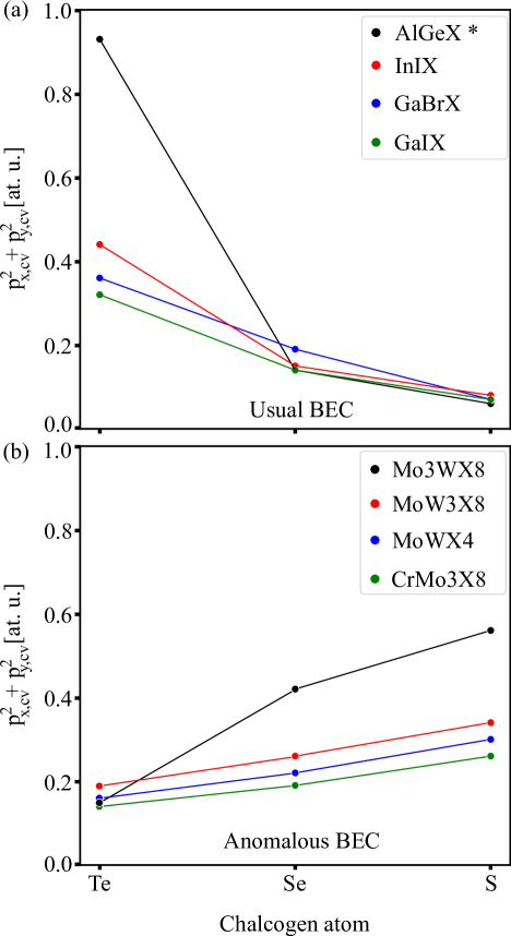
In Fig. 4, we present the values as a function of the chalcogen atom : Te, Se and S, for two representing groups of families of materials. The first group [Fig. 4(a)], consists of materials that exhibit the conventional Bader and BEC behaviour, i.e., their signs being equal. The only exception is the case of \ceAlGe, where the anomalous behaviour is partially presented, uniquely for the Ge atom. This group is composed by the families \ceAlGe (space-group no. 164), \ceInI (space-group no. 14), \ceGaBr (space-group no. 31) and \ceGaI (space-group no. 14). For all of these families the decreased optical coupling is evidenced when the chalcogen atom is more electronegative. On the other hand, the second group [Fig. 4(b)], consists of materials in which the anomalous BEC behavior is exhibited. It must be noted that for the latter group, cases containing the Te atom had no reported Bader charges; therefore, we performed their calculation and confirmed the anomalous behaviour (see Table. S2 from the SM [65]). The group is composed by the families \ceMo3W8, \ceMoW38, \ceMoW4 and \ceCrMo38, all belonging to the space-group no. 25. In this case, similarly to the behaviour presented by the TMDCs, the increased optical coupling is related to an increased electronegativity of the chalcogen atom, and the bonding mechanism responsible for the anomalous BEC is expected to account for the observed optical coupling values.
Finally, Fig. 2(h) illustrates the criterion vs values, distinguishing between materials with the anomalous BEC behavior from those with both Bader and BECs having the same sign across the entire ensemble of 2DMs. The analysis primarily focuses on , considering the in-plane charge response by means of the average of the and components of the Born effective charge tensor, defined as . Here, for each atom at position , the change in the component of the polarization is analyzed when the position is perturbed in the direction. Cross-terms of the Born effective charge tensor are excluded due to their low significance compared to the diagonal values, nor we consider the component. The selection of the trace of the reduced tensor is motivated by its invariance under basis transformations, thereby serving as a measure of the BEC magnitude. Furthermore, the focus is placed on the comparison between the sign of the BEC and the Bader charges. It should be emphasized that the relevant components of the BECs obtained from the C2DB and those reported by Pike et al. [58] for \ceMoS2, \ceMoSe2, \ceMoTe2 , \ceWS2 and \ceWSe2 are consistent. The results presented in Fig. 2(h) indicate that the bonding mechanism associated with the anomalous BEC behaviour could explain the high optical coupling values in the case of materials that deviate from the atomic selection rules for electronic transitions. In such materials, all atoms in the structure possess opposite signs of the Bader charges and BECs. Additionally, Fig. 2(h) presents instances in which at least one atom exhibits an opposite charge sign, while not all atoms do so. In such cases, the extension of the bonding mechanism should cautiously be evaluated and taken into account as a potential contributor to the strength of optical coupling.
IV Conclusions
We conducted a high-throughput study on the optical matrix elements between band edges of direct band gap, stable 2DMs. Our calculations revealed that approximately 37% of the materials examined exhibit symmetry forbidden optical transitions. Conversely, the materials with allowed optical transitions between the band edges exhibited a wide range of momentum matrix elements. Among them, 25% exclusively consist of p-block elements, while the remaining 75% are composed of materials that combine p-block and s-block and/or d-block elements. The highest value recorded for the optical coupling strength between the VBE and CBE, quantified by the in-plane momentum matrix elements was at.u. These values can be considered comparable to those observed in conventional bulk optoelectronic materials.
We proposed a numerical criterion, the allowed orbital overlap, based on the atomic selection rules for electronic transitions. The criterion employs information from the orbital projected Kohn-Sham states to quantify the optical coupling at the band edges of 2DMs. The application of the criterion to the materials ensemble demonstrated a high level of predictability in cases of materials with transitions at the k-point in the BZ, as well as in materials composed solely of elements from the p-block of the periodic table. On the other hand, the outlier analysis revealed distinctive characteristics of materials with a mixture of p- and d-block elements and its impact on the optical coupling between the VBE and CBE. These outliers exhibited transitions away from the high symmetry point in the BZ, and their crystal structures belonged to noncentrosymmetric space groups. We ruled out a direct correlation between the optical coupling and SOC and crystal-field splitting.
Finally, we conducted an analysis of the prominent group of monolayer TMDCs, which revealed a correlation between the optical coupling and the degree of bond ionicity or electron transfer in the material. We propose an explanation for the high optical coupling of these materials, related to the presence of a highly localized bond sensitive to atomic perturbations, and the cause of the anomalous BEC behavior. In traditional covalent semiconductors exhibiting the usual BEC situation, increased ionicity leads to lower optical coupling, as the electron hopping between atoms is reduced. In contrast, when the anomalous case is presented, more ionic systems lead to more charge involved in the highly localized bond, leading to more electron hopping between atoms and consequently an increase in optical coupling strength.
Acknowledgements.
A. F. G.-B. and O. R. acknowledge funding provided by the Natural Sciences and Engineering Research Council of Canada under the Discovery Grant Programs RGPIN-2020-04788 (application id 5017093). K. S. acknowledges the funding provided by the Mitacs Globalink program. Computing resources were provided by the Digital Research Alliance of Canada. A.C.G.C. acknowledges the grant entitled “Búsqueda y estudio de nuevos compuestos antiperovskitas laminares con respuesta termoeléctrica mejorada para su uso en nuevas energías limpias” supported by Vicerrectoría de Investigaciones y Extensión, VIE–UIS. Data availability The vasp input files required to reproduce the calculations, and the scripts used for the computation of the momentum matrix elements and the allowed orbital overlap criterion, are available in the Zenodo repository [104].References
- Novoselov [2011] K. S. Novoselov, Nobel lecture: Graphene: Materials in the flatland, Rev. Mod. Phys. 83, 837 (2011).
- Glavin et al. [2020] N. R. Glavin, R. Rao, V. Varshney, E. Bianco, A. Apte, A. Roy, E. Ringe, and P. M. Ajayan, Emerging applications of elemental 2D materials, Adv. Mater. 32, 1904302 (2020).
- Butler et al. [2013] S. Z. Butler, S. M. Hollen, L. Cao, Y. Cui, J. A. Gupta, H. R. Gutiérrez, T. F. Heinz, S. S. Hong, J. Huang, A. F. Ismach, E. Johnston-Halperin, M. Kuno, V. V. Plashnitsa, R. D. Robinson, R. S. Ruoff, S. Salahuddin, J. Shan, L. Shi, M. G. Spencer, M. Terrones, W. Windl, and J. E. Goldberger, Progress, challenges, and opportunities in two-dimensional materials beyond graphene, ACS Nano 7, 2898 (2013).
- Chaves et al. [2020] A. Chaves, J. G. Azadani, H. Alsalman, D. R. da Costa, R. Frisenda, A. J. Chaves, S. H. Song, Y. D. Kim, D. He, J. Zhou, A. Castellanos-Gomez, F. M. Peeters, Z. Liu, C. L. Hinkle, S.-H. Oh, P. D. Ye, S. J. Koester, Y. H. Lee, P. Avouris, X. Wang, and T. Low, Bandgap engineering of two-dimensional semiconductor materials, Npj 2D Mater. Appl. 4, 29 (2020).
- Ramasubramaniam [2012] A. Ramasubramaniam, Large excitonic effects in monolayers of molybdenum and tungsten dichalcogenides, Phys. Rev. B 86, 115409 (2012).
- Gutiérrez et al. [2013] H. R. Gutiérrez, N. Perea-López, A. L. Elías, A. Berkdemir, B. Wang, R. Lv, F. López-Urías, V. H. Crespi, H. Terrones, and M. Terrones, Extraordinary room-temperature photoluminescence in triangular \ceWS2 monolayers, Nano Lett. 13, 3447 (2013).
- Sang et al. [2019] D. K. Sang, B. Wen, S. Gao, Y. Zeng, F. Meng, Z. Guo, and H. Zhang, Electronic and optical properties of two-dimensional tellurene: From first-principles calculations, Nanomaterials 9, 1075 (2019).
- Buscema et al. [2014] M. Buscema, D. J. Groenendijk, S. I. Blanter, G. A. Steele, H. S. J. van der Zant, and A. Castellanos-Gomez, Fast and broadband photoresponse of few-layer black phosphorus field-effect transistors, Nano Lett. 14, 3347 (2014).
- Tran et al. [2014] V. Tran, R. Soklaski, Y. Liang, and L. Yang, Layer-controlled band gap and anisotropic excitons in few-layer black phosphorus, Phys. Rev. B 89, 235319 (2014).
- Wang et al. [2015] X. Wang, A. M. Jones, K. L. Seyler, V. Tran, Y. Jia, H. Zhao, H. Wang, L. Yang, X. Xu, and F. Xia, Highly anisotropic and robust excitons in monolayer black phosphorus, Nat. Nanotechnol. 10, 517 (2015).
- Mak et al. [2010] K. F. Mak, C. Lee, J. Hone, J. Shan, and T. F. Heinz, Atomically thin \ceMoS2: A new direct-gap semiconductor, Phys. Rev. Lett. 105, 136805 (2010).
- Mak et al. [2012] K. F. Mak, K. He, J. Shan, and T. F. Heinz, Control of valley polarization in monolayer \ceMoS2 by optical helicity, Nat. Nanotechnol. 7, 494 (2012).
- Sallen et al. [2012] G. Sallen, L. Bouet, X. Marie, G. Wang, C. R. Zhu, W. P. Han, Y. Lu, P. H. Tan, T. Amand, B. L. Liu, and B. Urbaszek, Robust optical emission polarization in \ceMoS2 monolayers through selective valley excitation, Phys. Rev. B 86, 081301(R) (2012).
- Splendiani et al. [2010] A. Splendiani, L. Sun, Y. Zhang, T. Li, J. Kim, C.-Y. Chim, G. Galli, and F. Wang, Emerging photoluminescence in monolayer \ceMoS2, Nano Lett. 10, 1271 (2010).
- Newaz et al. [2013] A. K. M. Newaz, D. Prasai, J. I. Ziegler, D. Caudel, S. Robinson, R. F. Haglund, Jr, and K. I. Bolotin, Electrical control of optical properties of monolayer \ceMoS2, Solid State Commun. 155, 49 (2013).
- Cao et al. [2012] T. Cao, G. Wang, W. Han, H. Ye, C. Zhu, J. Shi, Q. Niu, P. Tan, E. Wang, B. Liu, and J. Feng, Valley-selective circular dichroism of monolayer molybdenum disulphide, Nat. Commun. 3, 887 (2012).
- Zeng et al. [2012] H. Zeng, J. Dai, W. Yao, D. Xiao, and X. Cui, Valley polarization in \ceMoS2 monolayers by optical pumping, Nat. Nanotechnol. 7, 490 (2012).
- Wang et al. [2018a] G. Wang, Y. Zhang, C. You, B. Liu, Y. Yang, H. Li, A. Cui, D. Liu, and H. Yan, Two dimensional materials based photodetectors, Infrared Phys. Technol. 88, 149 (2018a).
- Wang et al. [2018b] F. Wang, Z. Wang, L. Yin, R. Cheng, J. Wang, Y. Wen, T. A. Shifa, F. Wang, Y. Zhang, X. Zhan, and J. He, 2D library beyond graphene and transition metal dichalcogenides: a focus on photodetection, Chem. Soc. Rev. 47, 6296 (2018b).
- Gao et al. [2023] M. Gao, L. Yu, Q. Lv, F. Kang, Z.-H. Huang, and R. Lv, Photoluminescence manipulation in two-dimensional transition metal dichalcogenides, J. Mater. 9, 768 (2023).
- Li et al. [2020] Y. Li, H. Sun, L. Gan, J. Zhang, J. Feng, D. Zhang, and C.-Z. Ning, Optical properties and light-emission device applications of 2-D layered semiconductors, Proc. IEEE 108, 676 (2020).
- Xie et al. [2021] K. Xie, X. Li, and T. Cao, Theory and ab initio calculation of optically excited states—recent advances in 2D materials, Adv. Mater. 33, 1904306 (2021).
- Zhao et al. [2015] H. Zhao, Q. Guo, F. Xia, and H. Wang, Two-dimensional materials for nanophotonics application, Nanophotonics 4, 128 (2015).
- Bernardi et al. [2017] M. Bernardi, C. Ataca, M. Palummo, and J. C. Grossman, Optical and electronic properties of two-dimensional layered materials, Nanophotonics 6, 479 (2017).
- Fox [2010] M. Fox, Optical properties of solids, 2nd ed. (Oxford University Press, 2010).
- Cohen and Louie [2019] M. L. Cohen and S. G. Louie, Fundamentals of condensed matter physics (Cambridge University Press, 2019).
- Yu and Cardona [2016] P. Yu and M. Cardona, Fundamentals of semiconductors: Physics and materials properties (Springer, 2016).
- Kormányos et al. [2015] A. Kormányos, G. Burkard, M. Gmitra, J. Fabian, V. Zólyomi, N. D. Drummond, and V. Fal’ko, K · p theory for two-dimensional transition metal dichalcogenide semiconductors, 2D Mater. 2, 022001 (2015).
- Masakatsu Suzuki and Takeshi Uenoyama [1996] M. S. Masakatsu Suzuki and T. U. Takeshi Uenoyama, Theoretical study of momentum matrix elements of \ceGaN, Jpn. J. Appl. Phys. 35, 543 (1996).
- Shokhovets et al. [2005] S. Shokhovets, G. Gobsch, and O. Ambacher, Momentum matrix element and conduction band nonparabolicity in wurtzite \ceGaN, Appl. Phys. Lett. 86, 161908 (2005).
- Rhim et al. [2005] S. H. Rhim, M. Kim, A. J. Freeman, and R. Asahi, Fully first-principles screened-exchange LDA calculations of excited states and optical properties of III-V semiconductors, Phys. Rev. B 71, 045202 (2005).
- Hermann and Weisbuch [1977] C. Hermann and C. Weisbuch, kp perturbation theory in III-V compounds and alloys: a reexamination, Phys. Rev. B 15, 823 (1977).
- Pfeffer and Zawadzki [1996] P. Pfeffer and W. Zawadzki, Five-level kp model for the conduction and valence bands of \ceGaAs and \ceInP, Phys. Rev. B 53, 12813 (1996).
- Cardona et al. [1988] M. Cardona, N. E. Christensen, and G. Fasol, Relativistic band structure and spin-orbit splitting of zinc-blende-type semiconductors, Phys. Rev. B 38, 1806 (1988).
- Vurgaftman et al. [2001] I. Vurgaftman, J. R. Meyer, and L. R. Ram-Mohan, Band parameters for III-V compound semiconductors and their alloys, J. Appl. Phys. 89, 5815 (2001).
- Dresselhaus et al. [2010] M. S. Dresselhaus, G. Dresselhaus, and A. Jorio, Group theory: Application to the physics of condensed matter (Springer, 2010).
- Lynch [1997] D. W. Lynch, Handbook of Optical Constants of Solids (Academic Press, 1997).
- Gupta et al. [2024] M. Gupta, S. Jana, and B. R. K. Nanda, Electronic structure and optoelectronic properties of halide double perovskites: Fundamental insights and design of a theoretical workflow, Chem. Mater. 36, 132 (2024).
- Li and Appelbaum [2014] P. Li and I. Appelbaum, Electrons and holes in phosphorene, Phys. Rev. B Condens. Matter Mater. Phys. 90, 115439 (2014).
- Wang et al. [2017a] G. Wang, C. Robert, M. M. Glazov, F. Cadiz, E. Courtade, T. Amand, D. Lagarde, T. Taniguchi, K. Watanabe, B. Urbaszek, and X. Marie, In-plane propagation of light in transition metal dichalcogenide monolayers: Optical selection rules, Phys. Rev. Lett. 119, 047401 (2017a).
- Meng et al. [2017] W. Meng, X. Wang, Z. Xiao, J. Wang, D. B. Mitzi, and Y. Yan, Parity-forbidden transitions and their impact on the optical absorption properties of lead-free metal halide perovskites and double perovskites, J. Phys. Chem. Lett. 8, 2999 (2017).
- Appadurai et al. [2021] T. Appadurai, R. Kashikar, P. Sikarwar, S. Antharjanam, B. R. K. Nanda, and A. K. Chandiran, Manipulation of parity and polarization through structural distortion in light-emitting halide double perovskites, Commun. Mater. 2, 1 (2021).
- Kato et al. [2020] M. Kato, M. Nishiwaki, and H. Fujiwara, Very high oscillator strength in the band-edge light absorption of zincblende, chalcopyrite, kesterite, and hybrid perovskite solar cell materials, Phys. Rev. Mater. 4, 035402 (2020).
- Bader [1985] R. F. W. Bader, Atoms in molecules, Acc. Chem. Res. 18, 9 (1985).
- Maier et al. [2020] S. Maier, S. Steinberg, Y. Cheng, C.-F. Schön, M. Schumacher, R. Mazzarello, P. Golub, R. Nelson, O. Cojocaru-Mirédin, J.-Y. Raty, and M. Wuttig, Discovering electron‐transfer‐driven changes in chemical bonding in lead chalcogenides (\cePb, where \ce = \ceTe, \ceSe, \ceS, \ceO), Adv. Mater. 32, 2005533 (2020).
- Wuttig et al. [2022] M. Wuttig, C.-F. Schön, M. Schumacher, J. Robertson, P. Golub, E. Bousquet, C. Gatti, and J.-Y. Raty, Halide perovskites: Advanced photovoltaic materials empowered by a unique bonding mechanism, Adv. Funct. Mater. 32, 2110166 (2022).
- Schön et al. [2022] C.-F. Schön, S. van Bergerem, C. Mattes, A. Yadav, M. Grohe, L. Kobbelt, and M. Wuttig, Classification of properties and their relation to chemical bonding: Essential steps toward the inverse design of functional materials, Sci. Adv. 8, eade0828 (2022).
- Zhang et al. [2023] X. Zhang, Y. Guo, D. Chu, and J. Robertson, Enhanced photovoltaic properties of halide perovskites due to multi-centered X–B–X bonding and p–p orbital coupling, J. Appl. Phys. 133, 115701 (2023).
- Tran et al. [2015] V. Tran, R. Fei, and L. Yang, Quasiparticle energies, excitons, and optical spectra of few-layer black phosphorus, 2D Mater. 2, 044014 (2015).
- Laurien and Rubel [2022] M. Laurien and O. Rubel, Benchmarking exchange-correlation potentials with the mstar60 dataset: Importance of the nonlocal exchange potential for effective mass calculations in semiconductors, Phys. Rev. B. 106, 045204 (2022).
- Blood [2015] P. Blood, Quantum Confined Laser Devices: Optical gain and recombination in semiconductors, 1st ed. (Oxford University Press, London, England, 2015).
- Hohenberg and Kohn [1964a] P. Hohenberg and W. Kohn, Inhomogeneous electron gas, Phys. Rev. 136, B864 (1964a).
- Kohn and Sham [1965a] W. Kohn and L. J. Sham, Self-consistent equations including exchange and correlation effects, Phys. Rev. 140, A1133 (1965a).
- Haastrup et al. [2018] S. Haastrup, M. Strange, M. Pandey, T. Deilmann, P. S. Schmidt, N. F. Hinsche, M. N. Gjerding, D. Torelli, P. M. Larsen, A. C. Riis-Jensen, J. Gath, K. W. Jacobsen, J. Jørgen Mortensen, T. Olsen, and K. S. Thygesen, The computational 2D materials database: high-throughput modeling and discovery of atomically thin crystals, 2D Mater. 5, 042002 (2018).
- Gjerding et al. [2021] M. N. Gjerding, A. Taghizadeh, A. Rasmussen, S. Ali, F. Bertoldo, T. Deilmann, N. R. Knøsgaard, M. Kruse, A. H. Larsen, S. Manti, T. G. Pedersen, U. Petralanda, T. Skovhus, M. K. Svendsen, J. J. Mortensen, T. Olsen, and K. S. Thygesen, Recent progress of the computational 2d materials database (C2DB), 2D Mater. 8, 044002 (2021).
- Woods-Robinson et al. [2023] R. Woods-Robinson, Y. Xiong, J.-X. Shen, N. Winner, M. K. Horton, M. Asta, A. M. Ganose, G. Hautier, and K. A. Persson, Designing transparent conductors using forbidden optical transitions, Matter 6, 3021 (2023).
- Wełnic et al. [2007] W. Wełnic, S. Botti, L. Reining, and M. Wuttig, Origin of the optical contrast in phase-change materials, Phys. Rev. Lett. 98, 236403 (2007).
- Pike et al. [2017] N. A. Pike, B. Van Troeye, A. Dewandre, G. Petretto, X. Gonze, G.-M. Rignanese, and M. J. Verstraete, Origin of the counterintuitive dynamic charge in the transition metal dichalcogenides, Phys. Rev. B 95, 201106(R) (2017).
- Hohenberg and Kohn [1964b] P. Hohenberg and W. Kohn, Inhomogeneous electron gas, Phys. Rev. 136, B864 (1964b).
- Kohn and Sham [1965b] W. Kohn and L. J. Sham, Self-consistent equations including exchange and correlation effects, Phys. Rev. 140, A1133 (1965b).
- Kresse and Hafner [1993] G. Kresse and J. Hafner, Ab initio molecular dynamics for liquid metals, Phys. Rev. B 47, 558 (1993).
- Kresse and Furthmüller [1996] G. Kresse and J. Furthmüller, Efficiency of ab-initio total energy calculations for metals and semiconductors using a plane-wave basis set, Comput. Mater. Sci. 6, 15 (1996).
- Blöchl [1994] P. E. Blöchl, Projector augmented-wave method, Phys. Rev. B 50, 17953 (1994).
- Perdew et al. [1996] J. P. Perdew, K. Burke, and M. Ernzerhof, Generalized gradient approximation made simple, Phys. Rev. Lett. 77, 3865 (1996).
- [65] See Supplemental Material at URL-will-be-inserted-by-publisher for the pseudopotential details, convergence tests, linear regression, chemical trend analysis and Bader charges calculation details. Refs included are [54, 55, 105, 106, 107, 108].
- Steiner et al. [2016] S. Steiner, S. Khmelevskyi, M. Marsmann, and G. Kresse, Calculation of the magnetic anisotropy with projected-augmented-wave methodology and the case study of disordered \ceFe_CO_, Phys. Rev. B 93, 224425 (2016).
- Rubel and Blaha [2022] O. Rubel and P. Blaha, Length-gauge optical matrix elements in WIEN2k, Computation 10, 22 (2022).
- Tonndorf et al. [2013] P. Tonndorf, R. Schmidt, P. Böttger, X. Zhang, J. Börner, A. Liebig, M. Albrecht, C. Kloc, O. Gordan, D. R. T. Zahn, S. M. de Vasconcellos, and R. Bratschitsch, Photoluminescence emission and Raman response of monolayer \ceMoS2, \ceMoSe2, and \ceWSe2, Opt. Express 21, 4908 (2013).
- Lu et al. [2017] A.-Y. Lu, H. Zhu, J. Xiao, C.-P. Chuu, Y. Han, M.-H. Chiu, C.-C. Cheng, C.-W. Yang, K.-H. Wei, Y. Yang, Y. Wang, D. Sokaras, D. Nordlund, P. Yang, D. A. Muller, M.-Y. Chou, X. Zhang, and L.-J. Li, Janus monolayers of transition metal dichalcogenides, Nat. Nanotechnol. 12, 744 (2017).
- Kappera et al. [2014] R. Kappera, D. Voiry, S. E. Yalcin, B. Branch, G. Gupta, A. D. Mohite, and M. Chhowalla, Phase-engineered low-resistance contacts for ultrathin \ceMoS2 transistors, Nat. Mater. 13, 1128 (2014).
- Lopez-Sanchez et al. [2013] O. Lopez-Sanchez, D. Lembke, M. Kayci, A. Radenovic, and A. Kis, Ultrasensitive photodetectors based on monolayer \ceMoS2, Nat. Nanotechnol. 8, 497 (2013).
- Wang et al. [2017b] Y. Wang, J. Xiao, H. Zhu, Y. Li, Y. Alsaid, K. Y. Fong, Y. Zhou, S. Wang, W. Shi, Y. Wang, A. Zettl, E. J. Reed, and X. Zhang, Structural phase transition in monolayer \ceMoTe2 driven by electrostatic doping, Nature 550, 487 (2017b).
- Tongay et al. [2014] S. Tongay, H. Sahin, C. Ko, A. Luce, W. Fan, K. Liu, J. Zhou, Y.-S. Huang, C.-H. Ho, J. Yan, D. F. Ogletree, S. Aloni, J. Ji, S. Li, J. Li, F. M. Peeters, and J. Wu, Monolayer behaviour in bulk \ceReS2 due to electronic and vibrational decoupling, Nat. Commun. 5, 3252 (2014).
- Okada et al. [2014] M. Okada, T. Sawazaki, K. Watanabe, T. Taniguch, H. Hibino, H. Shinohara, and R. Kitaura, Direct chemical vapor deposition growth of \ceWS2 atomic layers on hexagonal boron nitride, ACS Nano 8, 8273 (2014).
- Island et al. [2014] J. O. Island, M. Buscema, M. Barawi, J. M. Clamagirand, J. R. Ares, C. Sánchez, I. J. Ferrer, G. A. Steele, H. S. J. van der Zant, and A. Castellanos-Gomez, Ultrahigh photoresponse of few-layer \ceTiS3 nanoribbon transistors, Adv. Opt. Mater. 2, 641 (2014).
- Dresselhaus et al. [1955] G. Dresselhaus, A. F. Kip, and C. Kittel, Cyclotron resonance of electrons and holes in silicon and germanium crystals, Phys. Rev. 98, 368 (1955).
- Kane [1957] E. O. Kane, Band structure of indium antimonide, J. Phys. Chem. Solids 1, 249 (1957).
- de Carvalho et al. [2011] L. C. de Carvalho, A. Schleife, and F. Bechstedt, Influence of exchange and correlation on structural and electronic properties of \ceAlN, \ceGaN, and \ceInN polytypes, Phys. Rev. B 84, 195105 (2011).
- Heyd et al. [2003] J. Heyd, G. E. Scuseria, and M. Ernzerhof, Hybrid functionals based on a screened Coulomb potential, J. Chem. Phys. 118, 8207 (2003).
- Krukau et al. [2006] A. V. Krukau, O. A. Vydrov, A. F. Izmaylov, and G. E. Scuseria, Influence of the exchange screening parameter on the performance of screened hybrid functionals, J. Chem. Phys. 125, 224106 (2006).
- Tran and Blaha [2011] F. Tran and P. Blaha, Implementation of screened hybrid functionals based on the Yukawa potential within the LAPW basis set, Phys. Rev. B 83, 235118 (2011).
- Shokhovets et al. [2008] S. Shokhovets, O. Ambacher, B. K. Meyer, and G. Gobsch, Anisotropy of the momentum matrix element, dichroism, and conduction-band dispersion relation of wurtzite semiconductors, Phys. Rev. B 78, 079902(E) (2008).
- Aspnes [1976] D. E. Aspnes, \ceGaAs lower conduction-band minima: Ordering and properties, Phys. Rev. B 14, 5331 (1976).
- Adolph et al. [1996] B. Adolph, V. I. Gavrilenko, K. Tenelsen, F. Bechstedt, and R. Del Sole, Nonlocality and many-body effects in the optical properties of semiconductors, Phys. Rev. B 53, 9797 (1996).
- Cohen and McEachran [1972] M. Cohen and R. P. McEachran, Length and velocity formulae in approximate oscillator strength calculations, Chem. Phys. Lett. 14, 201 (1972).
- Starace [1973] A. F. Starace, Comment on “Length and velocity formulas in approximate oscillator-strength calculations”, Phys. Rev. A. 8, 1141 (1973).
- Bechstedt [2016] F. Bechstedt, Many-body approach to electronic excitations: Concepts and applications (Springer, Berlin, Germany, 2016).
- Martin [2020] R. Martin, Electronic structure: Basic theory and practical methods, 2nd ed. (Cambridge University Press, Cambridge, England, 2020).
- Onida et al. [2002] G. Onida, L. Reining, and A. Rubio, Electronic excitations: density-functional versus many-body Green’s-function approaches, Rev. Mod. Phys. 74, 601 (2002).
- Rohlfing et al. [2000] M. Rohlfing, S. G. Louie, and L. B. Materials Science Division, Electron-hole excitations and optical spectra from first principles, Phys. Rev. B 62, 4927 (2000).
- Benedict et al. [1998] L. X. Benedict, E. L. Shirley, and R. B. Bohn, Optical absorption of insulators and the electron-hole interaction: An ab initio calculation, Phys. Rev. Lett. 80, 4514 (1998).
- Wegner [1980] F. Wegner, Inverse participation ratio in 2+ dimensions, Z Physik B 36, 209 (1980).
- Murphy et al. [2011] N. C. Murphy, R. Wortis, and W. A. Atkinson, Generalized inverse participation ratio as a possible measure of localization for interacting systems, Phys. Rev. B 83, 184206 (2011).
- Pashartis and Rubel [2017] C. Pashartis and O. Rubel, Localization of electronic states in III-V semiconductor alloys: A comparative study, Phys. Rev. Appl. 7, 064011 (2017).
- Fox [2006] M. Fox, Quantum optics: An introduction. Oxford master series in physics (Oxford University Press, 2006).
- Cohen-Tannoudji [2006] C. Cohen-Tannoudji, Quantum Mechanics, 2 Volume Set (John Wiley & Sons, 2006).
- Rödl and Bechstedt [2012] C. Rödl and F. Bechstedt, Optical and energy-loss spectra of the antiferromagnetic transition metal oxides \ceMnO, \ceFeO, \ceCoO, and \ceNiO including quasiparticle and excitonic effects, Phys. Rev. B 86, 235122 (2012).
- Cotton [1990] F. A. Cotton, Chemical applications of group theory, 3rd ed. (John Wiley & Sons, 1990).
- Miessler et al. [2013] G. L. Miessler, P. J. Fischer, and D. A. Tarr, Inorganic chemistry: Pearson new international edition, 5th ed. (Pearson Education, 2013).
- Xiao et al. [2012] D. Xiao, G.-B. Liu, W. Feng, X. Xu, and W. Yao, Coupled spin and valley physics in monolayers of \ceMoS and other group-VI dichalcogenides, Phys. Rev. Lett. 108, 196802 (2012).
- Bernardi et al. [2013] M. Bernardi, M. Palummo, and J. C. Grossman, Extraordinary sunlight absorption and one nanometer thick photovoltaics using two-dimensional monolayer materials, Nano Lett. 13, 3664 (2013).
- Huisman et al. [1971] R. Huisman, R. de Jonge, C. Haas, and F. Jellinek, Trigonal-prismatic coordination in solid compounds of transition metals, J. Solid State Chem. 3, 56 (1971).
- Kumar and Ahluwalia [2012] A. Kumar and P. K. Ahluwalia, A first principle comparative study of electronic and optical properties of 1H – \ceMoS2 and 2H – \ceMoS2, Mater. Chem. Phys. 135, 755 (2012).
- Gomez-Bastidas et al. [2024] A. F. Gomez-Bastidas, K. Sriram, A. C. Garcia-Castro, and O. Rubel, Understanding the chemical and structural variability in the efficiency of band edge optical transitions of 2D monolayer materials (workflows) (2024), doi:10.5281/zenodo.13773214.
- Yu and Trinkle [2011] M. Yu and D. R. Trinkle, Accurate and efficient algorithm for Bader charge integration, J. Chem. Phys 134, 064111 (2011).
- Henkelman et al. [2006] G. Henkelman, A. Arnaldsson, and H. Jónsson, A fast and robust algorithm for bader decomposition of charge density, Computational Materials Science 36, 354 (2006).
- Tang et al. [2009] W. Tang, E. Sanville, and G. Henkelman, A grid-based bader analysis algorithm without lattice bias, J. Phys. Condens. Matter 21, 084204 (2009).
- Sanville et al. [2007] E. Sanville, S. D. Kenny, R. Smith, and G. Henkelman, Improved grid-based algorithm for bader charge allocation, J. Comput. Chem. 28, 899 (2007).
Understanding the chemical and structural variability in the efficiency of band edge optical transitions of 2D monolayer materials
Authors: A. F. Gomez-Bastidas†, Karthik Sriram†,∗, A. C. Garcia-Castro‡ and Oleg Rubel†
Affiliations: †Department of Materials Science and Engineering, McMaster University, 1280 Main Street West, Hamilton, Ontario L8S 4L8, Canada; ‡School of Physics, Universidad Industrial de Santander, Carrera 27 Calle 09, Bucaramanga, Santander 680002, Colombia. ∗ Department of Metallurgical and Materials Engineering, Indian Institute of Technology Madras, Chennai 600036, India.
S1 Pseudopotential valency and cutoff energy information
| Atom | Cutoff energy (eV) | Valency |
| H | 250 | 1 |
| Li_sv | 499 | 3 |
| C | 400 | 4 |
| N | 400 | 5 |
| O | 400 | 6 |
| F | 400 | 7 |
| Na_pv | 260 | 7 |
| Mg_pv | 404 | 8 |
| Al | 240 | 3 |
| Si | 245 | 4 |
| P | 255 | 5 |
| S | 259 | 6 |
| Cl | 262 | 7 |
| K_sv | 259 | 9 |
| Ca_sv | 267 | 10 |
| Sc_sv | 223 | 11 |
| Ti_sv | 275 | 12 |
| V_sv | 264 | 13 |
| Cr_pv | 266 | 12 |
| Mn_pv | 270 | 13 |
| Fe | 268 | 8 |
| Co | 268 | 9 |
| Ni | 270 | 10 |
| Cu_pv | 369 | 17 |
| Zn | 277 | 12 |
| Ga_d | 283 | 13 |
| Ge_d | 310 | 14 |
| As | 209 | 5 |
| Se | 212 | 6 |
| Br | 216 | 7 |
| Rb_sv | 220 | 9 |
| Sr_sv | 229 | 10 |
| Zr_sv | 230 | 12 |
| Nb_sv | 293 | 13 |
| Mo_sv | 243 | 14 |
| Ru_pv | 240 | 14 |
| Rh_pv | 247 | 15 |
| Pd | 251 | 10 |
| Ag | 250 | 11 |
| Cd | 274 | 12 |
| In_d | 239 | 13 |
| Sn_d | 241 | 14 |
| Sb | 172 | 5 |
| Te | 175 | 6 |
| I | 176 | 7 |
| Cs_sv | 220 | 9 |
| Ba_sv | 187 | 10 |
| Hf_pv | 220 | 10 |
| Ta_pv | 224 | 11 |
| W_sv | 223 | 14 |
| Re | 226 | 7 |
| Os | 228 | 8 |
| Ir | 211 | 9 |
| Pt | 230 | 10 |
| Au | 230 | 11 |
| Hg | 233 | 12 |
| Tl_d | 237 | 13 |
| Pb_d | 238 | 14 |
| Bi_d | 243 | 15 |
S2 Convergence tests
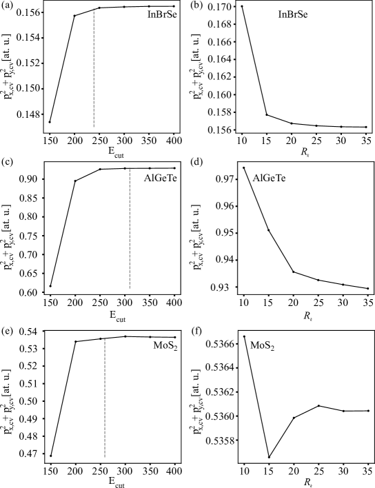
In Fig. S1, we present the in-plane momentum matrix elements plotted against the cuttoff energy and computational parameters for three representative materials from the 2DMs ensemble. In Fig. S1(a, c, e), we analyze convergence of the matrix elements with respect to the cutoff energy. For this analysis, a k-mesh was employed along with the accurate precision mode (PREC=accurate). The dashed lines indicate the values selected for each case in the high throughput calculation. On the other hand, in Figs. S1(b, d, f), we examine convergence of the momentum matrix elements with respect to the density of k-mesh points. The cutoff energy and the precision mode used in these calculations is consistent with the details provided in Sec. II of the main text. Additionally, calculations utilizing vasp’s normal precision mode (PREC=normal) were performed for comparative purposes. With this selection the number of points in the fast Fourier transform grid along the lattice parameter, . The differences between the squared momentum matrix elements obtained using the normal mode and the accurate mode were found to be negligible.
S3 Linear regression
S4 Optical coupling strength chemical trends analysis
Figure S3 presents the relationship between various factors and the in-plane momentum matrix elements. In Fig. S3(a) we analyze the electronegativity (Pauli’s scale) of the chalcogen atom. It is expected that higher values of electronegativity difference in binary compounds would result in higher ionicity due to electronic charge transfer between atoms. In Fig. S3(b) we present the Bader charge of the TM atom. Positive charge values indicate an electronic charge transfer from the TM atom to the chalcogen atoms. For each TM case the degree of electron transfer increases in the upward direction of the chalcogens (group 16) in the periodic table. The Bader charges from the chalcogen atom are not presented in this plot due to charge conservation. Finally in Fig. S3(c), we analyze the average of the in-plane components of the Born effective charge tensor of the transition metal atom. The magnitude of the BECs indicates the change in polarization due to the displacement of the atom from its equilibrium position. An equivalent definition of the BEC is the force induced on an ion by a uniform small electric field. In this manner, this physical quantity provides a measure of the dynamical charge on an ion. In this case, lowered BEC charge values correspond to higher optical coupling. It must be noted that the Bader and BECs were obtained from the C2DB database for our analysis [54, 55].
S5 Bader charges
In Table S2, we present the Bader charges computed for \ceCrMo3Te8, \ceMo2W2Te8, \ceMo3WTe8 and \ceMoW3Te8 2DMs, which were highlighted in Fig. 4(b) of the main text but for which no reported values are available. For comparison, we also present the BECs, which exhibit an opposite sign to the Bader charges in all instances, demonstrating the anomalous behavior. The Bader charges were computed employing the bader software [105, 106, 107, 108]. We employed the same computational parameters outlined in Sec. II of the main text. A significant parameter for the calculation of Bader charges is the ’fine’ fast Fourier transform grid NG(X, Y, Z)F, which is utilized for the representation of localized augmentation charges. In our calculations the precision mode selected was PREC=accurate, which defines the NG(X, Y, Z)F grid as twice the fast Fourier transform grid NG(X, Y, Z). To validate the results, the Bader charges were computed on denser grids, as detailed in Table S3. The variation of the charges magnitude between grids is approximately 5%; however, the relevant characteristic for the analysis, namely the sign of the charges, remains unchanged.
| \ceCrMo3Te8 | |
|---|---|
| (e) | 0.63, 0.52, 0.55, 0.55, -0.28, -0.28, -0.28, -0.28, -0.27, -0.29, -0.27, -0.29 |
| (e) | -3.83, -3.43, -3.38, -3.38, 1.46, 1.46, 1.83, 1.83, 1.83, 1.84, 1.89, 1.90 |
| \ceMo2W2Te8 | |
| (e) | 0.54, 0.54, 0.54, 0.54, -0.26, -0.28, -0.26, -0.28, -0.27, -0.28, -0.27, -0.28 |
| (e) | -3.38, -3.37, -2.52, -2.52, 1.41, 1.41, 1.41, 1.41, 1.54, 1.54, 1.54, 1.54 |
| \ceMo3WTe8 | |
| (e) | 0.54, 0.55, 0.54, 0.47, -0.26, -0.28, -0.25, -0.28, -0.25, -0.26, -0.25, -0.26 |
| (e) | -3.31, -3.31, -3.26, -2.54, 1.52, 1.52, 1.52, 1.52, 1.54, 1.54, 1.63, 1.64 |
| \ceMoW3Te8 | |
| (e) | 0.55, 0.53, 0.54, 0.54, -0.27, -0.27, -0.27, -0.27, -0.26, -0.27, -0.26, -0.27 |
| (e) | -3.39, -2.62, -2.56, -2.54, 1.32, 1.32, 1.40, 1.41, 1.42, 1.42, 1.42, 1.42 |
| FFT grid | (e) |
|---|---|
| 0.63, 0.52, 0.55, 0.55, -0.28, -0.28, -0.28, -0.28, -0.27, -0.29, -0.27, -0.29 | |
| 2 | 0.66, 0.58, 0.57, 0.57, -0.29, -0.29, -0.29, -0.29, -0.29, -0.30, -0.29, -0.30 |
| 3 | 0.68, 0.59, 0.59, 0.59, -0.30, -0.31, -0.31, -0.31, -0.30, -0.31, -0.30, -0.31 |