Size Effect on Raman Measured Stress and Strain Induced Phonon Shifts in Ultra-Thin Film Silicon
Abstract
The fabrication of complex nano-scale structures, which is a crucial step in the scaling of (nano) electronic devices, often leads to residual stress in the different layers present. This stress gradient can change many of the material properties and leads to desired or undesired effects, especially in the active part of the transistor, its channel. Measuring, understanding, and, ultimately, controlling the stress fields is hence crucial for many design steps.The level of stress can in principle be measured by micro-Raman spectroscopy. This, however, requires a priori knowledge of the mechanical properties of the material. The mechanical properties start to deviate from the bulk values when film dimensions become thinner than 5 nm. If this effect is ignored, errors of up to 400% can be introduced in the extracted stress profile. In this work, we illustrate this effect for a range of Si (001) slabs with different silicon film thickness, ranging from 5 to 0.7 nm and provide best practices for the proper interpretation of micro-Raman stress measurements.
Raman spectroscopy is a key characterization technique for measuring vibrational modes in biology, chemistry, and material science. The technique has proven to be an excellent non-invasive source of information in medicine, where it can identify protein morphologies and their structural evolution.[1, 2, 3, 4] In chemistry, surface-enhanced Raman scattering is a capable variant, which is able to detect vibrational signatures from single molecules, usually identified by fluorescence.[5, 6] In applications in solid state and semiconductor physics, Raman spectroscopy is also often used to determine the amount of stress engineered / present in the active component of a transistor. Using Raman peak shifts to determine stress, however, requires the a priory knowledge of the elastic [7, 8] or the Grüneisen tensor[9]. The wavelength of light gives an indication of penetration depth of the material, for example, infrared light can penetrate to a few m and at the UV wavelength it can be a few nm [10]. Using deep penetration within a surface, stress fields in different layers of nano structures can be measured with the additional advantage of being non-destructive. For reduced dimension, these start to deviate from their bulk values as quantified for free-standing ultra-thin films, observed in 2D systems,[11, 12] nano membranes,[13] and nanowires [14].
Since modern devices in nano electronics contain many material layers and have feature sizes on the order of 2-10 nm, interfacial or surface stresses become increasingly important. This is especially the case if the materials become less stiff in the confinement direction(s), i.e. yielding higher amounts of strain for the same unit of stress, under thinning. Since the conversion of the shifts in Raman frequencies into a stress tensor relies on the actual knowledge of the material elastic tensor, the question arises: without the quantification of the proper thickness dependence of the tensor, how much is the technique exaggerating the measured stress? In this letter, we address the problem in two ways. Firstly, by using existing knowledge of the elastic tensor variations with thinning. Secondly, we compute the shift of the peak phonon frequencies under external strain, using ab initio Si thin films models in the [001] direction with ABINIT [15, 16]. Therefore, it should be no surprise that there is also a size effect on the phonon frequencies of crystalline materials, yielding changing Raman shifts or broadening, which in tiny systems can be attributed to surface frequencies.[17, 18, 19]
.1 Overestimation Error Approximation
We begin our analysis by assessing the amount of overestimation by first estimating the extent of the effect by calculating the phonon shift with incident light polarized perpendicular to the surface on a film strained in the same direction (see Size Effect on Raman Measured Stress and Strain Induced Phonon Shifts in Ultra-Thin Film Silicon):
| (1) |
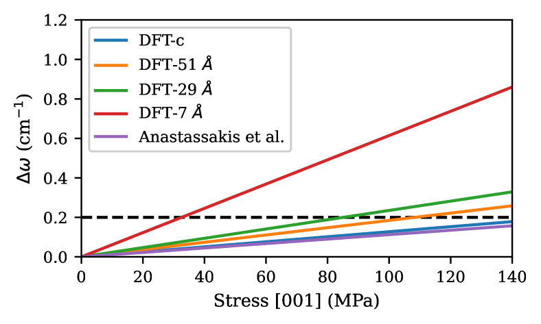
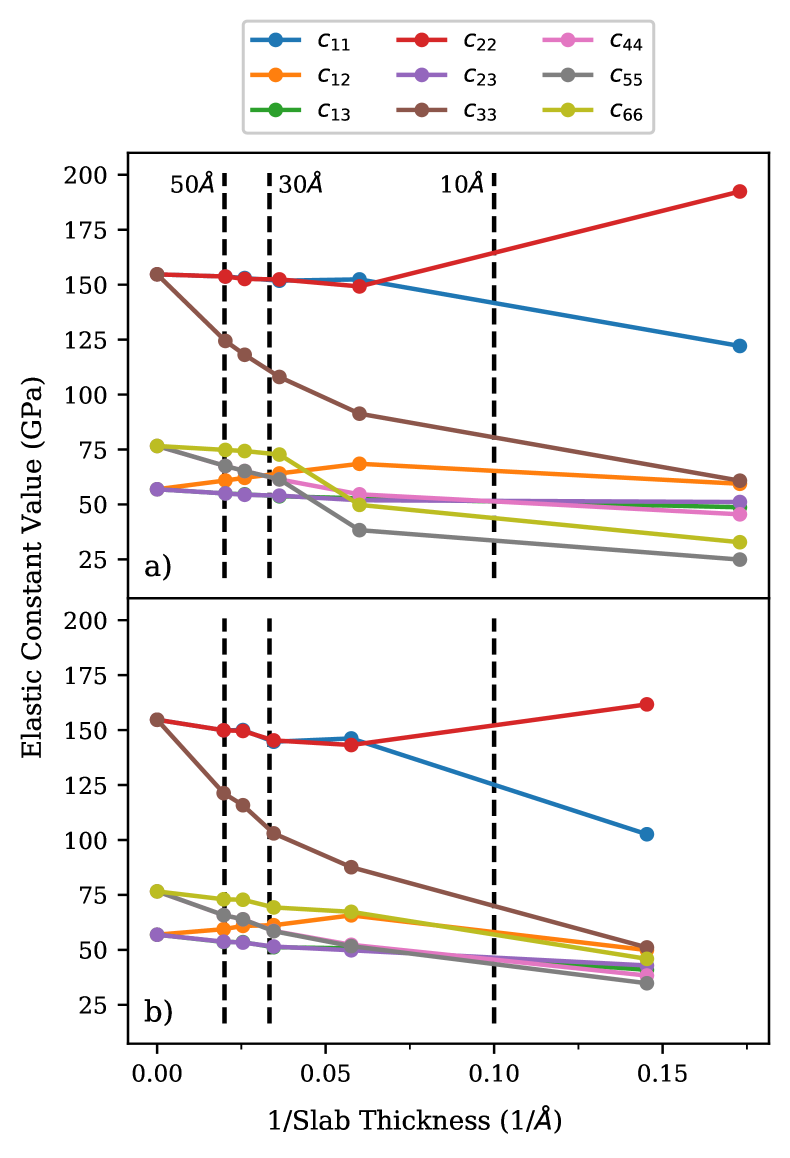
Here, we implicitly assume that the ultra-thin film has the same three-fold degenerate phonons as the primitive Si system (or 3 Raman active modes) and that the phonon deformation constants are the same as those of the bulk. We define as the third phonon frequency dependent on the Cauchy-stress component (the one in the direction of the thickness of the film), and as the non-perturbed phonon frequency. We report the Hartree-corrected elastic components for 1-5 nm Si films oriented in the [001] direction with dimer reconstruction in Table 1, see Size Effect on Raman Measured Stress and Strain Induced Phonon Shifts in Ultra-Thin Film Silicon for details. For a 1 nm Si film oriented with the vacuum in the Cartesian- direction, the () component reduces from 155 GPa in bulk to 51 GPa. Correspondingly, at 3 nm, the elastic tensor component was found to be 103 GPa and at 5 nm, it further increases to 121 GPa. Bulk Si has a peak phonon frequency of 520.5 cm-1 (observed at the -symmetry point in the Brillouin zone), with Phonon Deformation Potentials (PDPs) of and .[20, 21, 22] In Figure 1, it is observed that for the same magnitude of change in peak Raman frequency observed for a material under strain (), the DFT-computed free standing films yield far less stress than the bulk crystalline system.
| System | ||||||||||||
|---|---|---|---|---|---|---|---|---|---|---|---|---|
| Bulk | 155 | 114 | 114 | 114 | 155 | 114 | 114 | 114 | 155 | 77 | 77 | 77 |
| 51 Å | 150 | 119 | 107 | 119 | 150 | 107 | 107 | 107 | 121 | 66 | 66 | 73 |
| 29 Å | 145 | 122 | 102 | 122 | 145 | 103 | 102 | 103 | 103 | 59 | 58 | 69 |
| 7 Å | 103 | 100 | 82 | 100 | 162 | 86 | 82 | 86 | 51 | 38 | 35 | 46 |
As a relatively quick proof of concept, the experimental values of the bulk elastic tensor from Ref. [21] are used to compute the slopes and show good agreement with the computed crystalline system (blue line). The evaluation of the slopes of changing Raman shifts with externally applied stress demonstrates that if the PDPs do not change significantly, the stress in ultra-thin films in silicon device architecture is vastly overestimated. At its worst, the 1 nm equivalent film with a shift of 0.2 cm-1 has a stress of 33 MPa, whereas if the bulk compliance tensor was used on the same system, the corresponding stress is over 140 MPa - a factor of more than four increase. Even at a thickness of 5 nm, we obtain a corrected stress of 108 MPa, giving an error of over 30 MPa if the bulk parameters were used. Once again, the assumption takes for granted that the symmetry of the elastic tensor and PDP tensor remain equivalent in the bulk and in the free-standing film - which is evidently not the case. Regardless, this simple example neatly outlines how drastic the consequences of assuming the bulk properties when trying to quantify stresses in ultra-thin film materials may be; suggesting that a more in-depth approach to verify the variation in phonon frequencies corresponding to the Raman shifts is warranted.
.2 Bulk Phonon Shifts Under Strain
Instead of computing the elastic tensor and the phonon deformation potentials, the remaining portion of this letter focuses on directly calculating the phonon frequency shifts corresponding to Raman active modes, under externally applied strain. We first demonstrate that the correct phonon frequencies can be computed for cubic crystalline silicon. In the primitive unit cell of Si, consisting of two atoms, one would expect six phonon frequencies, three of which are the acoustic modes at 0 cm-1 with the other three being the optical frequencies near 520.5 cm-1.[20] Existing Density Functional Perturbation Theory (DFPT) calculations are in good agreement at 510.7 cm-1 using the PBEsol exchange correlation in Abinit.[23] Our calculations show good agreement with a peak average frequency of 506.4 cm-1, being about 3% smaller than the experimental value. However, we are primarily interested in the change in phonon frequencies corresponding to the shift in Raman peak frequencies in the Si (001) surface.
Compared to the 2-atom primitive cell of Si, since the cubic cell is not equivalent to the primitive cell, other Brillouin Zone (BZ) symmetry points are folded onto the -point giving the intermediate modes in between the expected modes. In the same manner, it is expected that some BZ points will wrap onto the -point in the surface model, even though its smallest unit of periodicity is the surface reconstruction. The eigenvectors and vibrational movement of atomic positions in bulk Si correspond to nearest atoms oscillating out-of-phase. This effectively creates a dipole oscillation resulting in a longitudinal optical phonon mode, the three maxima frequencies. These optical modes are those that are visible by the Raman scattering technique.
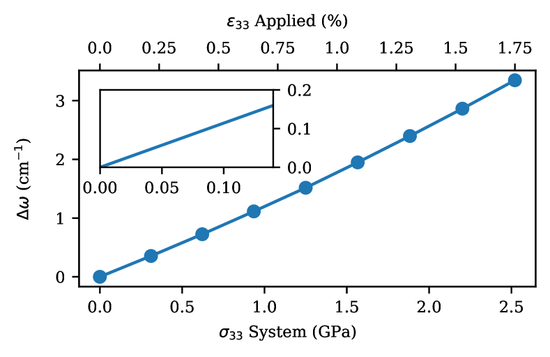
In order to compare to the exact same conditions of Figure 1, we are most concerned with the change in Raman peak frequencies in the same direction. This can be achieved by applying strain to the cubic cell along the [001] direction while the other lattice directions of [100] and [010] are allowed to contract and expand in order to minimize the stress in directions other than . Successive tensile strains ranging from 0 to 2% were applied to the system, as it tends to numerically perform in a more stable manner than compressive strains. The resulting stress from the material body can then be used in conjunction with the phonon analysis to reproduce the expected slope of Figure 1 for bulk crystalline Si. Figure 2 demonstrates the accuracy of the ab-initio calculation to detect shifts in the phonon frequency comparable with the experimental results. The inset shows the frequency shift as a function of the stress, in the same range as the earlier calculation with the elastic tensors. The change in phonon frequency (or Raman peak frequency) with the stress applied corresponds to 0.001142 cm-1MPa-1, which is in agreement with the experimental slope of the equivalent system setup of 0.001124 cm-1MPa-1 [21]. Reproducing the slope to within 1.6% difference suggests that using similar convergence parameters on a Si surface yields accurate results.
.3 Ultra-Thin Film Phonon Shifts Under Strain
To demonstrate the initial hypothesis that the phonon frequency shifts cannot be treated as bulk-like in the regime of ultra-thin films, frequencies of a clean free-standing slab of approximately 1 nm in thickness (i.e. 8 atomic layers) were calculated with the reconstruction surface in the (001) plane. These 32 atoms yield a total of 96 individual phonon frequencies, as observed in Figure 3. A single peak phonon frequency coincides with the bulk system. The increased number of modes is problematic since the optical modes must be distinguished to determine which phonon frequencies are considered to be Raman-active. In bulk Si the peak frequency is the only Raman active mode, however, in the ultra-thin film are more modes that are potentially active due to symmetry reduction and additional unique atomic sites. We assume in this paper that the predominant Raman active modes are those that are derived from the bulk peak, i.e., should yield a frequency close to the bulk -point. Therefore, we analyze the Raman modes within 20 cm-1 for the 1 nm system. Note that for the following discussion, the first mode of the system is denoted as the zeroth mode.
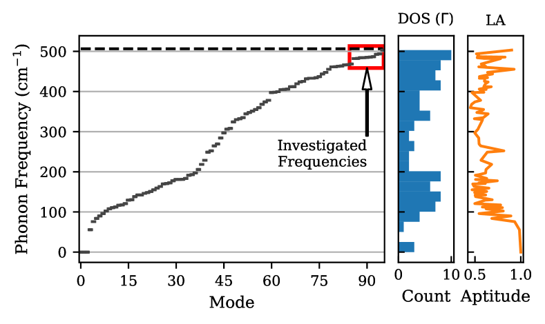
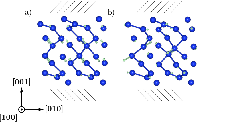
A quick analysis of the eigenvectors was performed to determine how longitudinal each mode is by taking the sum of the absolute value of inner product of each vector with every other vector (what we refer to in Figure 3 as LA). On average, the closer the sum is to unity, the more longitudinal the character of the phonon frequency is. By applying this scheme, the most energetic mode is longitudinal with a value of 0.90. This was verified by noticing that the eigenvectors or displacements of the phonons in Figure 4a) are predominantly bulk-like in motion. Recall that in the bulk, nearest neighbours oscillate forwards and backwards from each other, producing a LO phonon frequency. Typically, we observe that as the eigenfrequency becomes less, relative to the bulk-like mode, the system begins to prefer more movement near the surface. In Figure 4b), the next largest frequency is without doubt, not longitudinal and is less ordered. Typically, to determine if a mode is Raman-active, a dipole moment would be associated with the displacement pattern.[24] Alternatively, the Raman intensities can be directly computed ab-initio by calculating a few parameters such as the dielectric function.[25] The inclusion of vacuum in the unit cell complicates the Raman intensity calculation since the vacuum height scales the dielectric function, giving erroneous results. It can also quickly become a memory intensive application, so we choose not to compute the intensity here. [ref to the code we used to analyze, see materialsproject]
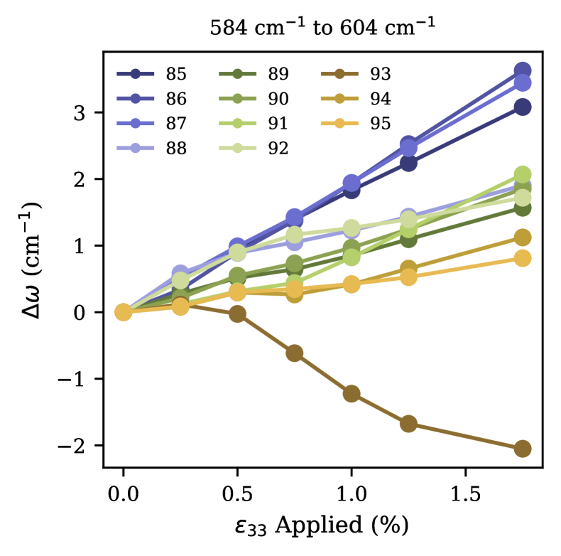
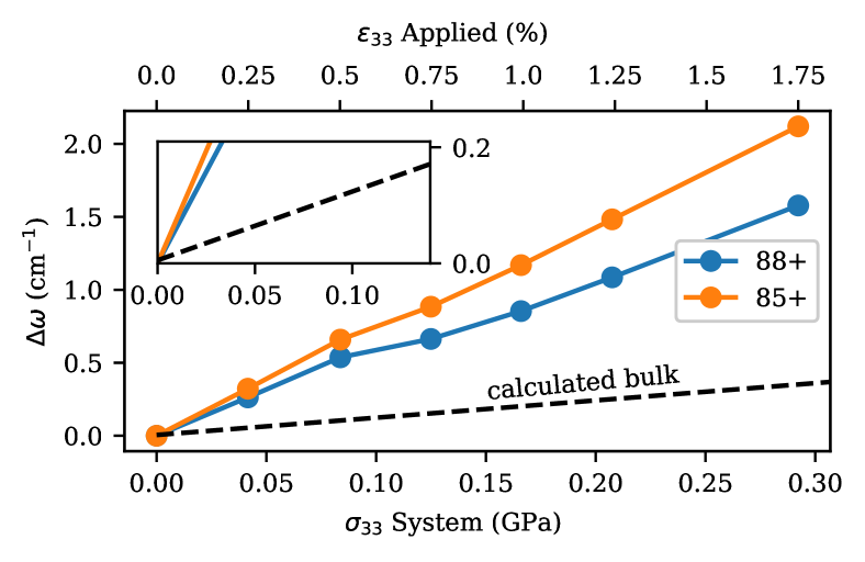
The modes within 20 cm-1 of the most energetic one are given in Figure 5 as a function of strain. With exception of the 93-rd mode, the phonon frequency shift is positive for a unit of compressive strain. This particular mode is characterized by a significant motion between the two layers of central atoms in the slab and may be due to a non-gamma centred mode wrapping onto the -point, though its displacement is similar to mode 94 which is slightly higher in energy by 4.5 cm-1. Given that the motion is similar to a higher energy mode (which points to a numerical issue), we choose to neglect it when calculating the mean phonon shift. Figure 6 shows the results of averaging the shift in phonon frequencies for two regimes: i) including the modes above the 88-th and ii) those above the 85-th, inclusively. The inset is centred in the same region as Figure 2 and verifies that the slope does increase; suggesting that for the same unit of stress applied to the system, a higher Raman peak frequency shift should be expected. For the 88-th mode analysis, the slope between the first two points is 0.006310 cm-1MPa-1 whereas since the 85-th mode includes higher shifts, the slope increases to 0.00775 cm-1MPa-1. When compared to the bulk crystalline expected relation of 0.001124 cm-1MPa-1, the slope is nearly 6 times the value due to the change introduced by the surface relative to the bulk centre of the film. Note that this may be an overestimation if the optical modes studied are not centred but instead wrapped from the Brillouin-zone, and should therefore not be included in the average top-most modes. Given that 32-atoms are required in the unit cell to capture the surface reconstruction effect, we believe these states to not be wrapped from the Brillouin-zone but being instead, an unique signature of the unit cell. Regardless, even considering just the highest eigenfrequency mode shifts, there is a significant difference in the shift/stress relation compared to the bulk.
.4 Best Practices
In order to use Raman spectroscopy effectively in material layers of 5 nm to measure stress, the elastic tensor must be re-evaluated first. Should there be significant interfaces of incredibly thin layers, expect the result to change even more.
.5 Summary
In this letter, we studied Raman peak shifts of silicon ranging from bulk to ultra-thin films using ab initio computations. We have shown that experimental PDPs combined with the elastic tensors of ultra-thin freestanding films calculated from Density Functional Theory, suggest that using Raman spectroscopy is vastly overestimating its characterization of the stress. We verified the calculation for bulk Si using ab-initio simulations to demonstrate that the phonon frequency shifts do indeed coincide with the expected Raman peak shifts under strain. Finally, by performing the same calculation as the bulk on free-standing ultra-thin film, we expect that indeed the Raman frequency shifts in a 1 nm thick layer can be up to 6 times larger for the same unit of applied stress or strain on the system. For packaged semiconductor devices, this result suggests that material layers are far more strained for significantly less stress. Assuming the bulk elastic tensor values for this characterization greatly overestimates the amount of stress.
I Acknowledgements
The various members of our group for discussions and aid over the course of this research. In particular, Ingrid De Wolf gave many valuable suggestions as to how to properly frame this work.
References
- Schulz and Baranska [2007] H. Schulz and M. Baranska, Vibrational Spectroscopy 43, 13 (2007).
- Wen [2007] Z.-Q. Wen, Journal of pharmaceutical sciences 96, 2861 (2007).
- Shashilov and Lednev [2009] V. A. Shashilov and I. K. Lednev, Journal of Raman Spectroscopy: An International Journal for Original Work in all Aspects of Raman Spectroscopy, Including Higher Order Processes, and also Brillouin and Rayleigh Scattering 40, 1749 (2009).
- Rygula et al. [2013] A. Rygula, K. Majzner, K. M. Marzec, A. Kaczor, M. Pilarczyk, and M. Baranska, Journal of Raman Spectroscopy 44, 1061 (2013).
- Nie and Emory [1997] S. Nie and S. R. Emory, science 275, 1102 (1997).
- Kneipp et al. [1997] K. Kneipp, Y. Wang, H. Kneipp, L. T. Perelman, I. Itzkan, R. R. Dasari, and M. S. Feld, Physical review letters 78, 1667 (1997).
- De Wolf [1996] I. De Wolf, Semiconductor science and technology 11, 139 (1996).
- De Wolf et al. [1996] I. De Wolf, H. Maes, and S. K. Jones, Journal of Applied Physics 79, 7148 (1996).
- Angel et al. [2019] R. J. Angel, M. Murri, B. Mihailova, and M. Alvaro, Zeitschrift für Kristallographie-Crystalline Materials 234, 129 (2019).
- Born and Wolf [2013] M. Born and E. Wolf, Principles of optics: electromagnetic theory of propagation, interference and diffraction of light (Elsevier, 2013).
- Lee et al. [2008] C. Lee, X. Wei, J. W. Kysar, and J. Hone, science 321, 385 (2008).
- Bertolazzi et al. [2011] S. Bertolazzi, J. Brivio, and A. Kis, ACS nano 5, 9703 (2011).
- Sarkar et al. [2021] A. Sarkar, Y. Lee, and J.-H. Ahn, Nano Research 14, 3010 (2021).
- Lee and Rudd [2007] B. Lee and R. E. Rudd, Physical Review B 75, 195328 (2007).
- Gonze et al. [2020] X. Gonze, B. Amadon, G. Antonius, F. Arnardi, L. Baguet, J.-M. Beuken, J. Bieder, F. Bottin, J. Bouchet, E. Bousquet, N. Brouwer, F. Bruneval, G. Brunin, T. Cavignac, J.-B. Charraud, W. Chen, M. Côté, S. Cottenier, J. Denier, G. Geneste, P. Ghosez, M. Giantomassi, Y. Gillet, O. Gingras, D. R. Hamann, G. Hautier, X. He, N. Helbig, N. Holzwarth, Y. Jia, F. Jollet, W. Lafargue-Dit-Hauret, K. Lejaeghere, M. A. L. Marques, A. Martin, C. Martins, H. P. C. Miranda, F. Naccarato, K. Persson, G. Petretto, V. Planes, Y. Pouillon, S. Prokhorenko, F. Ricci, G.-M. Rignanese, A. H. Romero, M. M. Schmitt, M. Torrent, M. J. van Setten, B. V. Troeye, M. J. Verstraete, G. Zérah, and J. W. Zwanziger, Comput. Phys. Commun. 248, 107042 (2020).
- Romero et al. [2020] A. H. Romero, D. C. Allan, B. Amadon, G. Antonius, T. Applencourt, L. Baguet, J. Bieder, F. Bottin, J. Bouchet, E. Bousquet, F. Bruneval, G. Brunin, D. Caliste, M. Côté, J. Denier, C. Dreyer, P. Ghosez, M. Giantomassi, Y. Gillet, O. Gingras, D. R. Hamann, G. Hautier, F. Jollet, G. Jomard, A. Martin, H. P. C. Miranda, F. Naccarato, G. Petretto, N. A. Pike, V. Planes, S. Prokhorenko, T. Rangel, F. Ricci, G.-M. Rignanese, M. Royo, M. Stengel, M. Torrent, M. J. van Setten, B. V. Troeye, M. J. Verstraete, J. Wiktor, J. W. Zwanziger, and X. Gonze, J. Chem. Phys. 152, 124102 (2020).
- Wang et al. [2001] S. Wang, W. Wang, J. Zuo, and Y. Qian, Materials Chemistry and Physics 68, 246 (2001).
- Choi et al. [2005] H. C. Choi, Y. M. Jung, and S. B. Kim, Vibrational spectroscopy 37, 33 (2005).
- Werninghaus et al. [1997] T. Werninghaus, J. Hahn, F. Richter, and D. Zahn, Applied physics letters 70, 958 (1997).
- Cerdeira et al. [1972] F. Cerdeira, C. Buchenauer, F. H. Pollak, and M. Cardona, Physical Review B 5, 580 (1972).
- Anastassakis et al. [1990] E. Anastassakis, A. Cantarero, and M. Cardona, Physical Review B 41, 7529 (1990).
- Tuschel [2019] D. Tuschel, Spectroscopy 34, 10 (2019).
- Petretto et al. [2018] G. Petretto, S. Dwaraknath, H. PC Miranda, D. Winston, M. Giantomassi, M. J. Van Setten, X. Gonze, K. A. Persson, G. Hautier, and G.-M. Rignanese, Scientific data 5, 1 (2018).
- Weber and Merlin [2000] W. H. Weber and R. Merlin, Raman scattering in materials science, Vol. 42 (Springer Science & Business Media, 2000).
- Gillet et al. [2013] Y. Gillet, M. Giantomassi, and X. Gonze, Phys. Rev. B 88, 094305 (2013).
- De Wolf [2015] I. De Wolf, Journal of Applied Physics 118, 053101 (2015).
- Schattke et al. [2003] W. Schattke, R. Bahnsen, and R. Redmer, Progress in Surface Science 72, 87 (2003).
- Pashartis et al. [2022] C. Pashartis, M. van Setten, M. Houssa, and G. Pourtois, Applied Surface Science 592, 153194 (2022).
- Umeno et al. [2005] Y. Umeno, A. Kushima, T. Kitamura, P. Gumbsch, and J. Li, physical Review B 72, 165431 (2005).
- Borštnik et al. [2014] U. Borštnik, J. VandeVondele, V. Weber, and J. Hutter, Parallel Computing 40, 47 (2014).
- Hutter et al. [2014] J. Hutter, M. Iannuzzi, F. Schiffmann, and J. VandeVondele, Wiley Interdisciplinary Reviews: Computational Molecular Science 4, 15 (2014).
- Guidon et al. [2008] M. Guidon, F. Schiffmann, J. Hutter, and J. VandeVondele, The Journal of Chemical Physics 128, 214104 (2008).
- Guidon et al. [2009] M. Guidon, J. Hutter, and J. VandeVondele, Journal of Chemical Theory and Computation 5, 3010 (2009).
- Guidon et al. [2010] M. Guidon, J. Hutter, and J. VandeVondele, Journal of Chemical Theory and Computation 6, 2348 (2010).
- Kühne et al. [2020] T. D. Kühne, M. Iannuzzi, M. Del Ben, V. V. Rybkin, P. Seewald, F. Stein, T. Laino, R. Z. Khaliullin, O. Schütt, F. Schiffmann, et al., The Journal of Chemical Physics 152, 194103 (2020).
- Goedecker et al. [1996] S. Goedecker, M. Teter, and J. Hutter, Physical Review B 54, 1703 (1996).
- Hartwigsen et al. [1998] C. Hartwigsen, S. Gœdecker, and J. Hutter, Physical Review B 58, 3641 (1998).
- Krack [2005] M. Krack, Theoretical Chemistry Accounts 114, 145 (2005).
- Perdew et al. [1996] J. P. Perdew, K. Burke, and M. Ernzerhof, Physical review letters 77, 3865 (1996).
- VandeVondele and Hutter [2007] J. VandeVondele and J. Hutter, The Journal of chemical physics 127, 114105 (2007).
Appendix A Appendix: Cubic Symmetry and Stress Characterization
The original derivation for what follows is modelled after unixial stress applied in the [110] direction by De Wolf 2015 [26], but is later extended to an orthorhombic system with strain (or its equivalent stress) in the [001] direction. For a system with diamond cubic symmetry such as silicon, the optical phonon modes, under the influence of strain, can be described by the direction of movement of the atoms in a lattice:
| (2) |
where are the elements of the force constant matrix, is the direction of movement of the atoms, and is the frequency of vibration. If the eigenvectors are along the directions (as the optical modes are for silicon), we can expand the force constant matrix in powers of the strain, ,
| (3) |
written in Einstein notation, up to first order. The new tensor and the elastic tensor are both fourth-order tensors and describe two different components of elasticity of a material system. is the so-called Phonon Deformation Potential (PDP) tensor, a material constant, whose values can be computed using ab-initio. The PDP is defined as the expectation value of the electron–phonon interaction potential.[27] Due to the symmetry of bulk silicon, the PDPs are known and given by three unique values (), in the same way that the elastic tensor is described by three values. They reduce the tensor to the same symmetry as the elastic one, giving,
| (4) |
With the consideration of Equation 4, Equation 2 can be reduced to the secular equation,
where the eigenvalues are described by . We now have a relationship that relates the strain, the PDPs, and the shift in phonon frequency from its natural state.
In its current state, the previous secular equation has no relation to the elastic tensor of silicon or the stress in a system. In order to link these quantities, recall that the stress tensor can be found from the strain of a system by,
| (5) |
or rewritten so that the strain can be replaced in the constitutive equations as
| (6) |
where is the Cauchy stress and S is the fourth-order symmetric compliance tensor such that it is the inverse of the elastic tensor (). Assuming only unixaxial stress is non-zero, , then the strains can be written as,
| (7) | ||||
Where all other strains are zero due to the symmetry of elastic tensor and due to the uniaxial stress condition, resulting in a diagonal determinant, giving three distinct solutions to the root after substitution,
| (8) | ||||
| (9) | ||||
| (10) | ||||
The result is one which suggests that the phonon frequency shifts detected under strain depend on both the stiffness of the system, the stress applied, and the natural frequency of the system. Depending on the direction and frequency of incident light, the excited phonon mode will differ. In the case of [001] incident polarized light, or light polarized along the Cartesian-, then only the third longitudinal optical peak will be observed, leaving only the equation. From here, depending on the stress in the system, the result can be further simplified. Current characterization using Raman spectroscopy relies on these material constants, in particular the bulk values, to measure the stress in complex semiconductor devices, but the stiffness of ultra-thin free-standing films or stacks of materials is not the same as in bulk.
Appendix B Appendix:Computation of Ultra-Thin Elastic Tensors
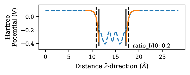
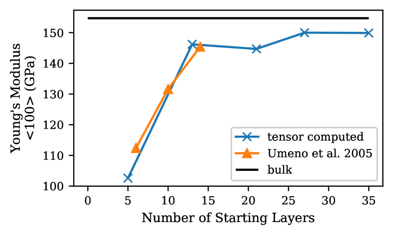
The procedure for calculating ultra-thin crystalline elastic tensors can be found in Ref. [28], where it was performed on Ru (001) films. The only difference between Ru and Si is the requirement of a larger unit cell to properly accommodate the surface reconstruction in the 2x1 [001] direction. For completeness we have plotted the elastic tensor as an evolution of thickness, with with the edge-to-edge thickness and the Hartree corrected scheme in Figure 7. The latter takes into account the extent of the Hartree potential extending past the surface compared to the bulk-type system, see reference. It is interesting to note that the proper trend for decreasing thickness is only observed with the corrected thickness schemed. The methodology was developed such that a consistent ratio can be defined over the same surface, regardless of thickness. In this case we determined a ratio of 0.2 (see Figure 8). As a proof of concept and to demonstrate that our tensor is correctly computed, we compare the tensor computed Young’s Modulus (which takes into account various components of the tensor) with DFT computed literature.
Elastic tensor calculations were performed using the first-principle CP2K simulation package [30, 31, 32, 33, 34, 35], using 3D periodic boundary conditions. A Fermi Dirac distribution for the occupancy of the valence band structure has been imposed with an electronic temperature of 1000 K. The Goedecker-Teter-Hutter CP2K pseudopotential library [36, 37, 38], was used and combined with the Perdew–Burke-Ernzerhof (PBE) [39] exchange correlation functional. DZVP basis sets were used from the CP2K standard library.[40] The simulations were converged with respect to the elastic tensor components for the bulk conventional structure to achieve a precision of 10 GPa. The bulk lattice parameters and elastic components were found to be converged with a k-point Monkhorst pack grid mesh of , a kinetic energy cutoff of 200 Ry and a relative energy cutoff of 50 Ry (for the Gaussian grid). The maximum force cutoff used for unit cell relaxation was 1E-4 bohr-1 Ha. Optimization was performed for the standard cubic unit cell of Si.