Measuring Chemical Shifts with Energy-Dispersive X-ray Spectroscopy
Abstract
Electron microscopy prevalently uses energy-dispersive x-ray spectroscopy (EDS) and electron energy loss spectroscopy (EELS) for elemental analysis. EDS and EELS energy resolutions are commonly between 30-100 eV or 0.01-1 eV, respectively. Large solid angle EDS detector technology has increased collection efficiency to enable precision spectroscopy via averaging of 0.02-0.1 eV. This improved precision gives access to chemical shifts; examples are shown in compounds of Al, Ti, and W. EDS can now detect chemical information in a complementary parameter space (accelerating voltage, thickness, atomic number) to that covered by EELS.
It is not enough to know what elements are present, their chemical bonding is also important. Transmission electron microscopy (TEM) can resolve atomic-level defects and interfaces inaccessible to other microscopy methods. These boundaries contain important chemical information Muller et al. (1993). X-ray spectroscopies for chemical detection, with energy resolution better than an eV, use absorption, emission, or photoelectrons and are spatially limited by x-ray sources and optics to micrometer probe sizes or greater Sánchez-López et al. (1998); Braun et al. (2002); Lindgren (2004). Spatial resolution using x-ray sources often does not surpass diffraction-limited optical microscope resolution Blomfield (2005). In the far field, only TEM can access elemental and chemical information at the atomic level.
Scanning transmission electron microscopy (STEM) rasters a sub-ångström sized probe to generate STEM images in parallel with techniques like energy-dispersive x-ray spectroscopy (EDS) and electron energy loss spectroscopy (EELS) Muller et al. (2008); Goodge et al. (2020); Zaluzec (2022, 2023). This pervasive pair of complementary spectroscopies measures the same inelastic events from different perspectives. EELS measures core electrons’ binding energies after a primary electron inelastically scatters from a quantum bound state into a magnetic prism that disperses electrons onto a camera. Combining high spatial and energy resolution delivers chemical shift mapping across atomically sharp interfaces Muller et al. (1993); Colliex et al. (2010). EDS collects the emitted photon when an electron from a higher shell fills the hole made vacant by ejection from the bound state via inelastic scattering. EDS has comparatively poor energy resolution to EELS, but can detect a wider variety of elements.
Electrons captured in EELS must pass through the sample. To keep the signal-to-background ratio (SBR) high the electrons should minimally scatter Egerton (2007, 2011). Sharp edges (e.g. scattering from s and p orbitals) are not commonly accessible at binding energies with large quantum numbers and high scattering angles. High scattering angles can be defined as , where 2%, 3%, and 4% for good, acceptable, and threshold ranges, respectively MacLaren et al. (2018) (Figure 1a, 111 = 1+KE/mec2, KE is the electron’s kinetic energy, me is the electron mass, and c is the speed of light). What is inaccessible to EELS can be complementarily captured by EDS. Samples thick and thin can both produce good x-ray spectroscopy, only limited by the overvoltage needed to excite the transition (Figure 1a). X-ray spectroscopy’s limited energy resolution has restricted it to elemental analysis. EDS chemical detection using electron sources, like that done using x-ray sources Lindgren (2004), can extend precision TEM spectroscopy into a new parameter space of thick samples, lower accelerating voltages, and transitions inaccessible to EELS.
Different x-ray spectrometer technologies have been used in TEM. Wavelength-dispersive x-ray spectroscopy (WDS) and microcalorimeters can both achieve sub-10 eV energy resolution Castaing (1951); Wollman et al. (2001). WDS circumscribes target, crystal analyzer, and detector along a Rowland circle. Through mechanical motion the analyser and detector move along the circumference to cover a broad range of energies. The limited solid angle, serial collection, and moving parts make WDS ineffective for TEMs. Microcalorimeters have cryogenic requirements and speed limitations making them (currently) unsuitable Wollman et al. (1998). Silicon drift detectors (SDD) Lechner et al. (1996) replaced silicon-lithium detectors Fitzgerald et al. (1968) due to their high speed, larger solid angles, and lack of cryogen requirements 222See Supplimentary Info (SI) section Solid State Detector Evolution.. SDD based EDS detectors are widely used on TEMs across the world and make up a large portion of the semiconductor industry’s TEM workflow.
EDS instrumentation is less expensive than EELS by roughly an order of magnitude and requires no electron optics or associated alignments, making it more accessible than nearly any other spectroscopy Zaluzec (2023). EDS’s high SBR, even with thick samples or low accelerating voltages, makes it suitable for both scanning electron microscopes (SEMs) and TEMs Goldstein et al. (1986). At 30 kV accelerating voltage, accessible to SEMs and TEMs, EDS can already access the L line of all naturally occurring elements, whereas EELS efficiency (as in Fig. 1a) is restricted to elements below roughly titanium in atomic number.
The SDD EDS Lechner et al. (1996) x-ray peak full width at half maximum (FWHM) is predominately determined by the electronic noise and shot noise fluctuation when converting photons into electron-hole pairs. An expression for this peak width measure is,
| (1) |
where 30 eV denotes the FWHM of the strobe peak (Fig. 1b), which arises from the electronic noise in the SDD Goulding (1977), denotes the natural line width of transition energy, which is typically a few eV and too small to matter in quadrature. The others parameterize the photon to electron-hole pair conversion. The Fano factor, , quantifies the ionization correlations in silicon Shockley (1961); Klein (1968). Parameters and 3.6 eV) are the x-ray energy and the silicon ionization energy, respectively Lechner and Strüder (1995); Kotov et al. (2018).
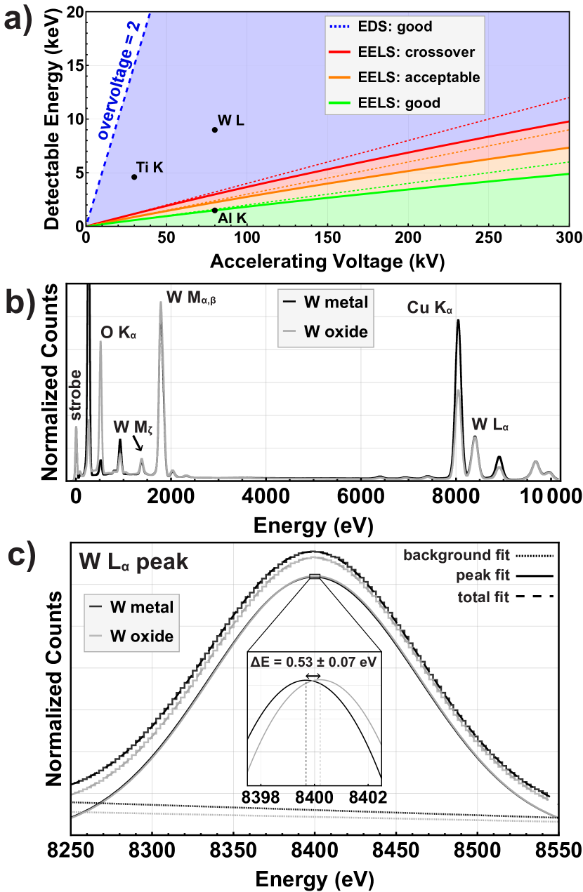
For a W x-ray peak around 8 keV (W for example, Fig. 1b), the EDS resolution 140 eV. This is two orders of magnitude larger than typical chemical shifts (a few eV or less) when compared linearly and much worse when added in quadrature. Insufficient resolution does not translate to insufficient precision. Since SDD are nearly shot noise limited, by averaging more x-ray events, the precision can be improved to a point where EDS becomes sensitive to sub-eV chemical shift. In Fig. 1c the measured chemical shift using curve fitting reveals a change just over half an eV 333See SI section Error Analysis of Energy for example fitting residuals. Despite EDS being unable to resolve chemical shifts at the level of natural linewidth resolution, by collecting enough counts in the shot noise limited regime better than 100 meV energy precision is achieved for well-isolated peaks 444The spectrometer bins and detector processing time are optimized to give the best precision and this process is discussed in the SI section Detector Optimization. With enhanced energy precision, EDS can be used for chemical shift measurement on heavy elements and even chemical shift mapping complementary to EELS.
To demonstrate EDS capability of measuring chemical shift, several compounds of tungsten (W), titanium (Ti), and aluminum (Al) are selected. The first two (acquired at at 80kV and 30kV, respectively) cover regions inaccessible with EELS. The three W compounds (Fig. 2a) and three Ti compounds (Fig. 2b) are commercially available nanoparticles deposited on transmission electron microscope (TEM) grids with a thin carbon film (<10 nm) using standard drop-casting methods 555See SI section on Sample Parameters for sample preparation and acquisition conditions.. An aluminum film and an aluminum oxide film are deposited on a silicon chip with silicon nitride electron-transparent window using electron-beam evaporation and atomic layer deposition respectively (Fig. 2c). The Al sample is micro-fabricated and the patterns of the two Al films are defined by optical lithography Hubbard et al. (2018). Having multiple compounds of the same metal element allows us to see how the transition energy is affected by different chemical environments.
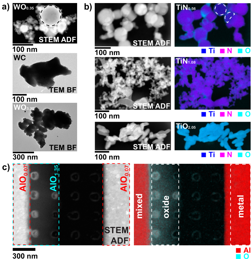
For each W specimen, a spectrum is acquired in the highlighted region of interest (ROI) or across the entire field of view (FOV). For an EDS spectrum like the one shown in Fig. 1b, the area under a certain peak is proportional to the abundance of the corresponding element, and any horizontal shift in the peak center is the chemical shift in the transition energy. For Fig. 2a top and bottom specimens, W Lα and O Kα peaks are used to determine the stoichiometry and measure the averaged valence of W. Following Cliff-Lorimer method Cliff and Lorimer (1975); Goldstein et al. (1986) and assuming oxygen having its most common valence -2, the composition is determined to be WO0.35 and WO3.30 respectively, which corresponds to a W averaged valence of +0.7 and +6.6 respectively. However, the carbon support membrane makes valence measurement infeasible for tungsten carbide (Fig. 2a middle), so we take the valence to be +4 according to the manufacturer’s 99.95 WC purity. For Ti and Al specimens, EDS spectrum images (where an EDS spectrum is acquired at each scan point in a raster pattern) are acquired, and elemental distributions are mapped. The valences of Al and Ti are determined the same way as the W specimens, and the chemical compositions are labelled in Fig. 2b,c 666A comparison of valence values are tabulated in the SI section on Sample Parameters.
The resolution of EDS is limited by the peak energy energy and electronic noise (Eq. 1). An isolated peak can be measured more precisely than the FWHM just as the error in the mean decreases as die rolls are averaged. As the counts increase, curve fitting improves the precision similarly in a nonlinear way. This enhanced precision, typically three orders of magnitude better than the FWHM resolution, provides chemical shift detection in EDS. In the shot noise limited regime, the uncertainty carried by individual x-ray measurement disturbs the curve fitting and limits the precision. As the number of counts N increases, the precision goes up as a function of (Fig. 3a). This relationship is governed by Poisson statistics. As N increases, the precision vs counts curve flattens and approaches a limit. This asymptotic behavior arises from the signal-to-background ratio (SBR) which is independent of the number of counts collected.
Solid state EDS detectors measure x-ray energy by collecting induced charges. A derived expression, the energy precision as a function of counts, is shown in Eq. 2. Poisson noise from the counting process and precision limit contribute. The uncertainty comes from a single x-ray event. It is closely related to Equation (1) empirically by 777See section Detector Optimization is the SI for further analysis.. Because of fluctuations in the ionization process, photons with the same energy do not always generate the same number of charges Shockley (1961). This leads to the uncertainty which is x-ray energy dependent, and its contribution to the total uncertainty can be reduced by collecting more x-ray events Kallithrakas-Kontos (1996); Xiao et al. (1998). In the expression is described how precision changes as a function of counts,
| (2) |
represents highest precision can be achieved for a given peak, which is found to be negatively correlated with the SBR 888see SI section Detector Optimization for SBR details.. These two uncorrelated terms, and , add in quadrature and determine the total uncertainty of the measured x-ray energy. This empirical expression fits multiple datasets (Fig. 3a). X-ray events are rare (one x-ray photon is generated per ten thousand beam electrons Cosslett (1978)), but in solid state detectors collecting millions of counts is routine.
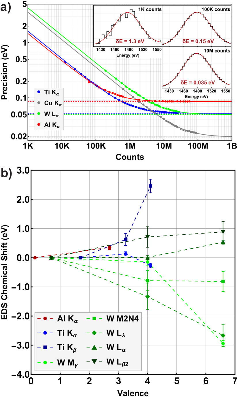
Unlike EELS, where chemical shifts in the binding energies are always positive, EDS chemical shift in the transition energies can be either positive or negative Lindgren (2004); Yao and Holst (1967); Burkhalter et al. (1972); Kawai et al. (1994); Braun et al. (2002); Boydaş et al. (2015); Miaja-Avila et al. (2021). In three W samples imaged at 80 kV, with 2.5 eV/channel bin size, chemical shifts are observed in five transitions lines ranging from 1 to 10 keV (Fig. 3b). The three W L lines all have an energy higher than 7 keV, which is above the crossover regime for EELS (Fig. 1a). W Lα and W Lβ2 have positive chemical shifts less than +1 eV (about 1/3 of a spectrometer bin), and W Lλ has a negative chemical shift down to -2.6 eV (about one bin). Chemical shifts are also observed in W Mγ and W M2N4 lines, both negatively signed. Because of the high elastic/inelastic scattering cross section ratio and a short mean free path, W edges are very difficult to measure precisely with EELS. As an atom forms more bonds, the energies of core electrons are further minimized, which results in higher binding energies Carpenter et al. (1982). So, EELS chemical shifts are always positive Sapre and Mande (1972). While EDS measures the energy difference between two electron orbits, whether the chemical shift is positive or negative depends on which electron’s energy is minimized more when forming a new chemical bond. If the energy of the electron with a lower orbit is minimized more, the EDS chemical shift is positive, and vice versa. Thus, the observation of both positive and negative chemical shift coincides with our expectation.
In spectrum images acquired on Ti samples, spectra are summed inside the ROI or across the entire FOV. For Fig. 2b top, a ROI is applied to select nanoparticles with low nitrogen concentration to differentiate from Fig. 2b middle sample. The peak energies of Ti Kα and Ti Kβ lines are measure by curve fitting. The Ti Kβ line shifts up to +2.4 eV (about one bin), while the Ti Kα shifts less than 0.5 eV (Fig. 3). Acquired at 30 kV accelerating voltage, the 5 keV lineline is well over the crossover regime for EELS (Fig. 1a), but EDS can still provide precise information about the K shell. W and Ti measurements in the parameter space of large transition line and low accelerating voltage are inaccessible with EELS. By measuring Al Kα line around 1.5 keV (which is accessible with other TEM methods), the results are comparable with the literature. The spectrum image shows three distinct regions: mixed, oxide, and metal region (Fig. 2c). The two ROIs in Fig. 2c bottom highlight the regions where only aluminum or aluminum oxide film exists. The spectra in the two ROIs are summed respectively, and the Al Kα chemical shift is determined to be +0.35 eV by curve fit, which is consistent with previous measurements Burkhalter et al. (1972); Lindgren (2004) (the shift is about 1/14 the bin size). A summary of the EDS chemical shifts is tabulated in the Supplementary Information.
Finally, to demonstrate our capability to map chemical shift, the aluminum EDS spectrum image is binned to have enough counts to fit the Al Kα line on pixel level. Three distinct regions are visible in the Al Kα energy map (Fig. 4a) together with the column-averaged plot (Fig. 4b). The oxide region having a higher transition energy than the metal region indicates the Al K shell energy is minimized more than the L shell during the oxidation. A smooth transition is observed between the oxide and the mixed region and an oxide edge is detected at the edge of the metal region (Fig. 4b). Even though the two peaks representing Al metal and oxide are not well-separated in the histogram (Fig. 4c), a skewed normal distribution (for Al metal) and a normal distribution (for Al oxide) can be fitted to the distribution, and a shift of +0.36 eV is measured this way between the peak centers. This measurement on the histogram is in excellent agreement with the summed spectra measurement shown in Fig. 3b. And it demonstrates that chemical shift mapping is possible with a 0.6 Sr solid angle single crystal detector 999Another example of mapping is shown in SI section EDS Chemical Shift Map..
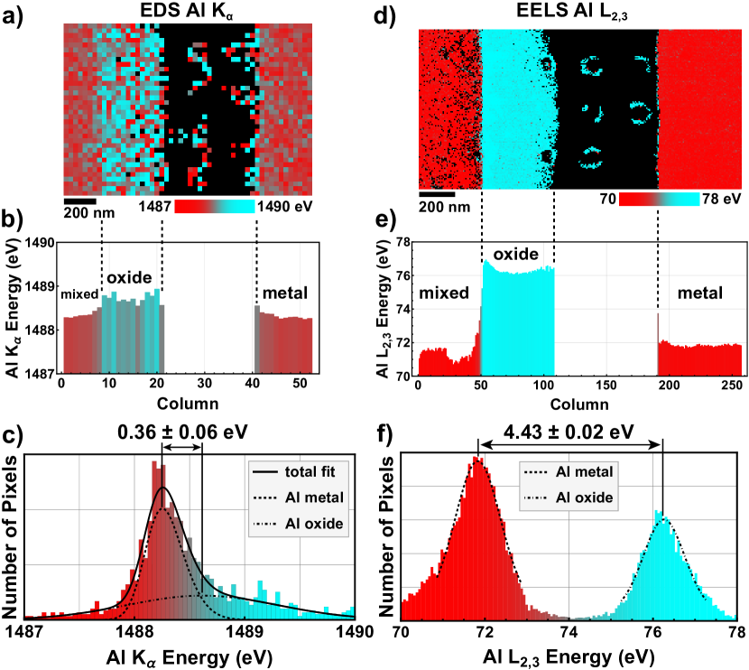
An EELS spectrum image is collected in the same region under the same microscope settings to compare with the EDS analysis. At 80 kV accelerating voltage, EELS is borderline “acceptable” for measuring Al K edge at 1.5 keV, so only the Al L2,3 edge (around 75 eV) is captured 101010An EELS chemical shift from the data in Fig. 4 is shown in Sup Fig. 10. The Al L2,3 edge, having a larger cross section, is much easier to map than the Al K edge. Because EELS is optically defined, the spectrum must be acquired quickly to avoid drift in the optical components. EDS can be mapped nearly indefinitely as spectra are not subjected to optical shifts. By measuring the Al L2,3 edge location, a similar set of energy map and plots are generated (Fig. 4d-f). Three distinct regions are visible in the EELS Al L2,3 energy map and column-averaged plot, and the two peaks for Al metal and oxide are well-separated in the histogram. EELS appearing to differentiate the metal and the oxide better is a result of the chemical shift in Al L2,3 edge being an order magnitude greater than that in the Al Kα transition. It does not imply EELS having a better energy precision. In fact, for the Al metal region, the EDS energy map has 3 times better precision. EDS Al Kα line measures the Al K-L2,3 transition energy, and EELS Al L2,3 edge measures the Al L2,3 binding energy. Combining them, the Al K 1s binding energy is determined to be 1559.95 0.03 eV for Al metal and 1564.88 0.04 eV for Al oxide, similar to results using EELS Sánchez-López et al. (1998). Being able to match EELS’ energy precision and access a much higher energy range, EDS is a great complementary for chemical shift analysis purposes. And in this specific case, EDS provides information EELS missing about the Al K shell with comparable precision.
Chemical analysis has long been the domain of EELS Egerton (2007, 2011). As the accelerating voltage is lowered, the range of energies accessible with EELS decreases monotonically. EDS, in contrast, does not suffer from these constraints. EDS can be used over a wide range of accelerating voltages, sample thicknesses, and atomic numbers. Moreover, an EELS spectrum is defined optically. The magnetic prism used to disperse electrons with different energies, although -metal armored, is highly susceptible to changes in the local magnetic field Egerton (2007). These changes, along with scan deflections, can shift the spectrum in energy space enough to cause a systematic effect that appears as a chemical shift. The zero-energy position in the EDS spectrum, not being optically defined, is nearly imperturbable, which allows adding spectra together from any time or position without any misalignment in energy Lechner et al. (1996). Typically, EDS (EELS) is acquired over many frames (one frame) and a drift correction applied between frames (rows). Last but not least, an EDS system is more than an order of magnitude cheaper than conventional EELS systems. All these factors, versatility, stability, and cost efficiency, make it desirable to extend chemical analysis into the domain of EDS.
Through collecting large numbers of counts, EDS chemical shifts can be measured from a variety of compounds with sub-100 meV precision. And the EDS chemical shifts in transition energies can be either positive or negative, depending on the specific transition and chemical environment. Furthermore, chemical shift mapping across an Al metal-oxide interface is demonstrated (Fig. 4a-c) with a common SDD. When used by itself, EDS can detect chemical shifts in transition lines with sub-100 meV precision. And when paired with EELS, EDS can extend chemical shift analysis in binding energies to one or two orders of magnitude higher energy, without requiring a higher accelerating voltage or any advanced electron optics. The spatial resolution of EDS chemical shift mapping, fundamentally limited by the sample dependent x-ray generation volume, ranges from atomic level (sub-ångström) to a few nanometers. Chemical shift maps in this work, limited by number of counts per unit area under the Al Kα peak, have a spatial resolution of about 30 nm. State-of-the-art SDDs can collect more than a million counts per second Zaluzec (2022). With such a detector, the minimal number of counts needed for chemical shift detection (10k per peak) can be collected in 100 ms. EDS chemical shifts, in addition to being important for electron microscopy, can also be used where in other system using the same spectroscopy technique, such as x-ray florescent imaging.
This work was supported by the Semiconductor Research Corporation (SRC), National Science Foundation (NSF) award DMR-1611036, and NSF STC award DMR-1548924 (STROBE). Data were collected at the Core Center of Excellence in Nano Imaging (University of Southern California), the Electron Imaging Center for Nanosystems (EICN) (RRID:SCR022900) at the University of California, Los Angeles’s California for NanoSystems Institute (CNSI), and the Thermo Fisher Scientific (TFS) Nanoport. Samples were fabricated in the Integrated Systems Nanofabrication Cleanroom (ISNC) at the California NanoSystems Institute (CNSI). We would like to thank Lee Casalena and Huikai Cheng for their help understanding and operating the TFS Spectra Ultra S/TEM with Ultra-X EDS.
References
- Muller et al. (1993) D. A. Muller, Y. Tzou, R. Raj, and J. Silcox, Nature 366, 725 (1993).
- Sánchez-López et al. (1998) J. C. Sánchez-López, A. Caballero, and A. Fernández, Journal of the European Ceramic Society 18, 1195 (1998).
- Braun et al. (2002) A. Braun, H. Wang, U. Bergmann, M. C. Tucker, W. Gu, S. P. Cramer, and E. J. Cairns, Journal of Power Sources 112, 231 (2002).
- Lindgren (2004) I. Lindgren, Journal of Electron Spectroscopy and Related Phenomena ICESS-9 Proceedings of the 9th International Conference on Electronic Spectroscopy and Structure, 137-140, 59 (2004).
- Blomfield (2005) C. J. Blomfield, Journal of Electron Spectroscopy and Related Phenomena Electron Energy Loss Spectroscopy in the Electron Microscope, 143, 241 (2005).
- Muller et al. (2008) D. A. Muller, L. F. Kourkoutis, M. Murfitt, J. H. Song, H. Y. Hwang, J. Silcox, N. Dellby, and O. L. Krivanek, Science 319, 1073 (2008), publisher: American Association for the Advancement of Science.
- Goodge et al. (2020) B. Goodge, A. Carlsson, M. Bischoff, A. Mohammadi-Gheidari, G. Fallag, G. Schwind, C. Maunders, D. Muller, and L. Kourkoutis, Microscopy and Microanalysis 26, 1508 (2020).
- Zaluzec (2022) N. J. Zaluzec, Microscopy and Microanalysis 28, 83 (2022), number: 1.
- Zaluzec (2023) N. J. Zaluzec, Microscopy and Microanalysis 29, 334 (2023).
- Colliex et al. (2010) C. Colliex, L. Bocher, F. de la Peňa, A. Gloter, K. March, and M. Walls, JOM 62, 53 (2010).
- Egerton (2007) R. F. Egerton, Ultramicroscopy 107, 575 (2007).
- Egerton (2011) R. F. Egerton, Electron Energy-Loss Spectroscopy in the Electron Microscope (Springer Science & Business Media, 2011) pp. 335–346.
- MacLaren et al. (2018) I. MacLaren, K. J. Annand, C. Black, and A. J. Craven, Microscopy 67, i78 (2018).
- Note (1) = 1+KE/mec2, KE is the electron’s kinetic energy, me is the electron mass, and c is the speed of light.
- Castaing (1951) R. Castaing, Application of electron probes to local chemical and crystallographic analysis, Ph.D. thesis, University of Paris (1951).
- Wollman et al. (2001) D. A. Wollman, S. W. Nam, G. C. Hilton, K. D. Irwin, D. A. Rudman, N. F. Bergren, S. Deiker, J. M. Martinis, M. E. Huber, and D. E. Newbury, AIP Conference Proceedings 550, 506 (2001).
- Wollman et al. (1998) D. A. Wollman, G. C. Hilton, K. D. Irwin, L. L. Dulcie, N. F. Bergren, D. E. Newbury, K.-S. Woo, B. Y. H. Liu, A. C. Diebold, and J. M. Martinis, AIP Conference Proceedings 449, 799 (1998).
- Lechner et al. (1996) P. Lechner, S. Eckbauer, R. Hartmann, S. Krisch, D. Hauff, R. Richter, H. Soltau, L. Strüder, C. Fiorini, E. Gatti, A. Longoni, and M. Sampietro, Nuclear Instruments and Methods in Physics Research Section A: Accelerators, Spectrometers, Detectors and Associated Equipment Proceedings of the Seventh European Symposium on Semiconductor, 377, 346 (1996).
- Fitzgerald et al. (1968) R. Fitzgerald, K. Keil, and K. F. J. Heinrich, Science 159, 528 (1968).
- Note (2) See Supplimentary Info (SI) section Solid State Detector Evolution.
- Goldstein et al. (1986) J. I. Goldstein, D. B. Williams, and G. Cliff, in Principles of Analytical Electron Microscopy, edited by D. C. Joy, A. D. Romig, and J. I. Goldstein (Springer US, Boston, MA, 1986) pp. 155–217.
- Goulding (1977) F. S. Goulding, Nuclear Instruments and Methods 142, 213 (1977).
- Shockley (1961) W. Shockley, Solid-State Electronics 2, 35 (1961).
- Klein (1968) C. A. Klein, IEEE Transactions on Nuclear Science 15, 214 (1968).
- Lechner and Strüder (1995) P. Lechner and L. Strüder, Nuclear Instruments and Methods in Physics Research Section A: Accelerators, Spectrometers, Detectors and Associated Equipment 354, 464 (1995).
- Kotov et al. (2018) I. V. Kotov, H. Neal, and P. O’Connor, Nuclear Instruments and Methods in Physics Research Section A: Accelerators, Spectrometers, Detectors and Associated Equipment 901, 126 (2018).
- Kohl and Reimer (2008) H. Kohl and L. Reimer, in Transmission Electron Microscopy: Physics of Image Formation, Springer Series in Optical Sciences (Springer, New York, NY, 2008) pp. 139–192.
- Note (3) See SI section Error Analysis of Energy for example fitting residuals.
- Note (4) The spectrometer bins and detector processing time are optimized to give the best precision and this process is discussed in the SI section Detector Optimization.
- Note (5) See SI section on Sample Parameters for sample preparation and acquisition conditions.
- Hubbard et al. (2018) W. A. Hubbard, M. Mecklenburg, H. L. Chan, and B. C. Regan, Physical Review Applied 10, 044066 (2018).
- Cliff and Lorimer (1975) G. Cliff and G. W. Lorimer, Journal of Microscopy 103, 203 (1975).
- Note (6) A comparison of valence values are tabulated in the SI section on Sample Parameters.
- Note (7) See section Detector Optimization is the SI for further analysis.
- Kallithrakas-Kontos (1996) N. Kallithrakas-Kontos, Spectrochimica Acta Part B: Atomic Spectroscopy 51, 1655 (1996).
- Xiao et al. (1998) Y. Xiao, S. Hayakawa, Y. Gohshi, and M. Oshima, Analytical Sciences 14, 1139 (1998).
- Note (8) See SI section Detector Optimization for SBR details.
- Cosslett (1978) V. E. Cosslett, Journal of Microscopy 113, 113 (1978).
- Yao and Holst (1967) T. C. Yao and J. J. Holst, Spectrochimica Acta Part B: Atomic Spectroscopy 23, 19 (1967).
- Burkhalter et al. (1972) P. G. Burkhalter, A. R. Knudson, D. J. Nagel, and K. L. Dunning, Physical Review A 6, 2093 (1972).
- Kawai et al. (1994) J. Kawai, T. Konishi, A. Shimohara, and Y. Gohshi, Spectrochimica Acta Part B: Atomic Spectroscopy 49, 725 (1994).
- Boydaş et al. (2015) E. Boydaş, E. Orhan, M. G. Boydaş, and E. Cömert, Procedia - Social and Behavioral Sciences World Conference on Technology, Innovation and Entrepreneurship, 195, 1757 (2015).
- Miaja-Avila et al. (2021) L. Miaja-Avila, G. C. O’Neil, Y. I. Joe, K. M. Morgan, J. W. Fowler, W. B. Doriese, B. Ganly, D. Lu, B. Ravel, D. S. Swetz, and J. N. Ullom, X-Ray Spectrometry 50, 9 (2021).
- Carpenter et al. (1982) R. W. Carpenter, I. Chan, H. L. Tsai, C. Varker, and L. J. Demer, MRS Online Proceedings Library 14, 195 (1982).
- Sapre and Mande (1972) V. B. Sapre and C. Mande, Journal of Physics C: Solid State Physics 5, 793 (1972).
- Note (9) Another example of mapping is shown in SI section EDS Chemical Shift Map.
- Note (10) An EELS chemical shift from the data in Fig. 4 is shown in Sup Fig. 10.