In-situ scanning gate imaging of individual two-level material defects in live superconducting quantum circuits
Abstract
The low temperature physics of structurally amorphous materials is governed by two-level system defects (TLS), the exact origin and nature of which remain elusive despite decades of study. Recent advances towards realising stable high-coherence platforms for quantum computing has increased the importance of studying TLS in solid-state quantum circuits, as they are a persistent source of decoherence and instability. Here we perform scanning gate microscopy on a live superconducting quantum circuit at millikelvin temperatures to locate individual TLS. Our method directly reveals the microscopic nature of TLS and is also capable of deducing the three dimensional orientation of individual TLS electric dipole moments. Such insights, when combined with structural information of the underlying materials, can help unravel the detailed microscopic nature and chemical origin of TLS, directing strategies for their eventual mitigation.
Glassy disordered materials show remarkable universality in their low-temperature thermal, acoustic and microwave absorption properties, irrespective of their chemical compositions Berthier and Biroli (2011); Leggett and Vural (2013). To explain these intriguing observations, Anderson et. al. and Phillips proposed the microscopic model of these materials to be dominated by low energy imperfections, namely, two-level system defects (TLS) Anderson et al. (1972); Phillips (1972), with their collective behaviour described by the phenomenological Standard Tunnelling Model (STM) Phillips (1987). However, in the half century since, direct probing of individual TLS defects and testing the microscopic principles underlying these macroscopic observations have been very challenging, fuelling intense debates over the exact nature of these defects Müller et al. (2019); Leggett and Vural (2013).
Though TLS have been extensively studied in glassy materials, recent advances in quantum computation and sensing have further underscored the need to characterise their chemical and structural properties Müller et al. (2019); de Graaf et al. (2022). TLS are a major source of noise and decoherence, and even a single defect can spoil the performance of an entire circuit Klimov et al. (2018); Müller et al. (2019); Mehmandoost and Dobrovitski (2024). Achieving fault tolerant quantum computing requires stable, high coherence qubits, which in turn need new tools to find, characterise, and understand the nature of TLS defects as they appear in live circuits. This task has been particularly challenging, as the low energy scales of the defects render them inaccessible to much of conventional material science techniques de Graaf et al. (2022).
Established in-operando methods of detecting TLS, for example by tuning a qubit into resonance with it Simmonds et al. (2004); Müller et al. (2019), or similarly tuning TLS by applying strain Grabovskij et al. (2012) or electric de Graaf et al. (2021); Lisenfeld et al. (2015); Bilmes et al. (2022, 2020, 2021); Lisenfeld et al. (2016, 2019); de Graaf et al. (2022) fields, are incapable of directly extracting precise defect locations. Furthermore, they only indirectly suggest the microscopic origin, revealing no chemical or structural information. On the other hand, traditional scanning probe techniques such as scanning tunnelling microscopy or atomic force microscopy (AFM) are routinely used for defect characterisation and offer atomic scale spatial resolution. Unfortunately, these techniques fall short by orders of magnitude in resolving the typical TLS energy scale. Despite this, scanning probe imaging of quantum circuits is becoming increasingly important for characterising electromagnetic field distributions and material properties in quantum devices at low temperatures Lang et al. (2004); Geaney et al. (2019); de Graaf et al. (2013); Zhang et al. (2024); Oh et al. (2021); Denisov et al. (2022); Marchiori et al. (2022).
Here we integrate scanning gate microscopy (SGM) with in-situ readout of live superconducting quantum circuits at millikelvin temperatures to locate individual TLS defects, directly demonstrating their microscopic nature. The SGM can also operate in AFM mode for imaging device topography. Furthermore, we also deduce the electric dipole moment orientation of individual TLS, information that has remained elusive since they were conceptually put forward over half a century ago. We posit that by combining information about TLS orientation with detailed material structure and ab-initio calculations, our approach could help identify the origin and physical nature of these defects, leading to better solid state quantum circuits.
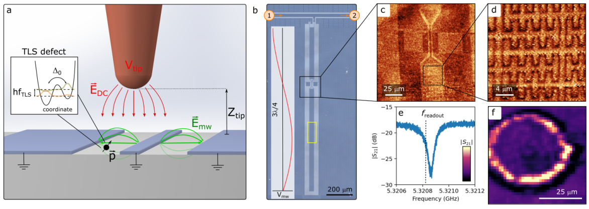
Our experimental setup combining SGM with in-situ device readout is described in the schematic presented in Fig. 1a. We use an electrochemically etched tungsten tip attached to a quartz tuning fork to facilitate AFM imaging. The tip is also connected to a voltage source for applying local electric fields in order to tune the energy of TLS. The entire setup is enclosed within a light-tight, magnetically shielded volume and suspended on springs below the mixing chamber plate of a dry dilution refrigerator to minimize vibrations. With this setup, we achieve a sample stage temperature of mK, as measured using a calibrated thermometer.
Although our SGM setup is entirely agnostic to the circuit under study and is adaptable for examining any quantum component coupled to TLS, here we choose to study a superconducting resonator. Our sample consists of a resonator patterned in 40 nm thick NbN on sapphire, an optical image of which is shown in Fig. 1b. Interdigitated capacitors concentrate the electric fields inside the resonator, enabling enhanced coupling to a large number of TLS defects. Further details about the sample can be found in Refs Mahashabde et al. (2020); Ranjan et al. (2022).
Figures 1c and 1d show AFM images of the live resonator obtained at 200 mK. This in-situ AFM imaging enables us to locate various device features. In all our experiments, we limit the scan speed to reduce heating of the piezo positioners and keep the sample temperature below 300 mK at all times, avoiding TLS saturation occurring for Lindström et al. (2009) or TLS bath reconfiguration de Graaf et al. (2020).
Following AFM imaging we locate individual TLS as follows. We position the tip at a constant height above the sample, and at each grid point in the xy-plane conduct a tip voltage sweep. We continuously, in operation, monitor the microwave (MW) signal transmitted at a fixed frequency slightly offset from the resonance frequency of the imaged device using a heterodyne detection measurement scheme (see Supplementary Information for details). A change in the measured signal thus means that either the resonator’s centre frequency or quality factor has changed, the result of a TLS becoming resonant with the resonator. The microwave power level used for transmission measurements was kept very low to avoid saturating TLS, typically with an average photon population of 10-1000 in the resonator. A slice of such a dataset is shown in Fig. 1f, where data from a pixel grid is presented. The observed ring indicates a locus of points at which the tip needs to be positioned for the TLS to experience the same electric field magnitude, to bring it into resonance with the resonator, i.e. the TLS is located at the centre of the ring. In the Supplementary Information, we show more data taken at high microwave powers that confirms the saturation of the detected TLS.
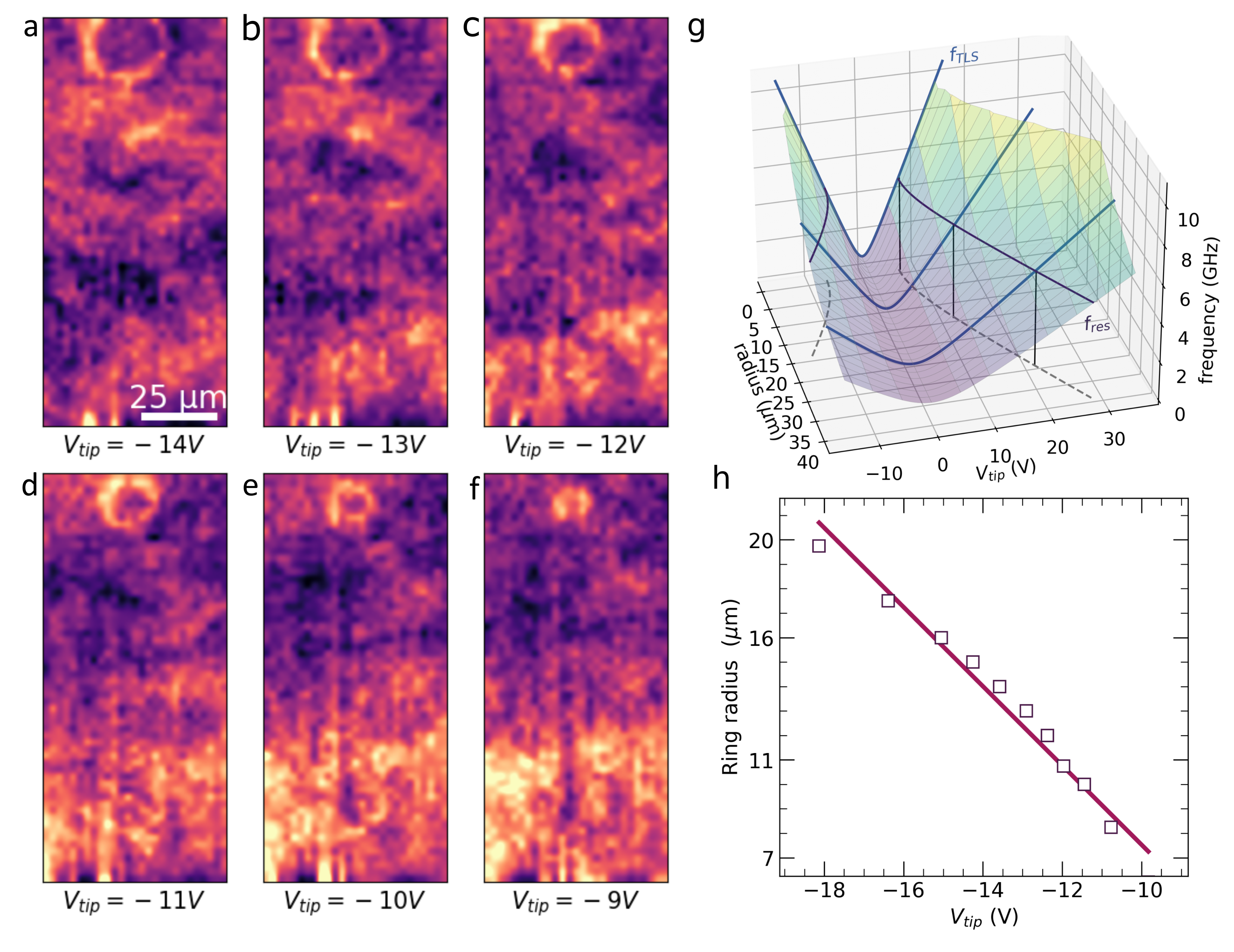
Varying the voltage at which the two-dimensional slice is taken changes the ring diameter, as shown in Fig. 2a-2f (for a different TLS than in Fig. 1f). This data was taken at m in the area of the yellow box in Fig. 1b. In addition to the clear circular contour, we also note the fluctuating background arising from other nearby TLS outside the grid frame. The grid data was collected over three days, implying the observed ring and other experimental parameters remained stable throughout. All panels of Fig. 2a-2f have had a parabolic background subtracted to remove the capacitive contribution of the tip on the resonator, which typically gives a much larger (but independent of tip voltage) response than TLS. Reversing the tip voltage sweep direction does not affect the shape or location of the ring, ruling out any charging effects on the device.
To understand why TLS manifest as rings in our experiment, we consider a TLS with an electric dipole moment interacting with the microwave field of a galvanically grounded resonator resulting in a coupling strength . When a sharp AFM tip with a DC voltage is positioned at a distance from the TLS, the defect experiences an electric field , causing a shift in its energy level transition frequency
| (1) |
where is the TLS asymmetry energy and is an offset energy imposed by the TLS’s local environment Lisenfeld et al. (2019). As the tip voltage is swept, the TLS frequency is tuned along this hyperbolic trajectory (plotted as blue lines in Fig. 2g). When the TLS becomes resonant with the resonator frequency (black curves in Fig 2g), it can be detected as a change in the measured signal. The contours traced out when moving the tip in the xy-plane are a set of points where the TLS experiences the same electric field magnitude. For the ring shown in Fig. 2, a smaller (larger) tip voltage changes the distance at which the tip must be placed for the TLS’s frequency to be shifted to be resonant with the resonator, and this results in a smaller (larger) ring. This shrinking of the ring with increasing tip voltage is also demonstrated in Fig. 2h, where we show that the radius of the ring in Fig. 2a-2f decreases linearly with the applied tip voltage for ring radii , as expected from Eq. (1).
As the tip voltage is increased, in most cases, we expect to observe either a shrinking or a growing ring. For very large tip voltages one could expect to see two concentric contours originating from each of the two intersection points of with the TLS hyperbola (Fig. 2h). These could be either both shrinking or both growing with increasing tip voltage. A third possibility is that one contour is shrinking, followed by one that is growing. These three scenarios depend on at what electric field strength with respect to zero field the TLS minima is located. In the experiment, we kept below to prevent damaging the tip or sample, and hence, so far have only observed either shrinking or growing single rings.
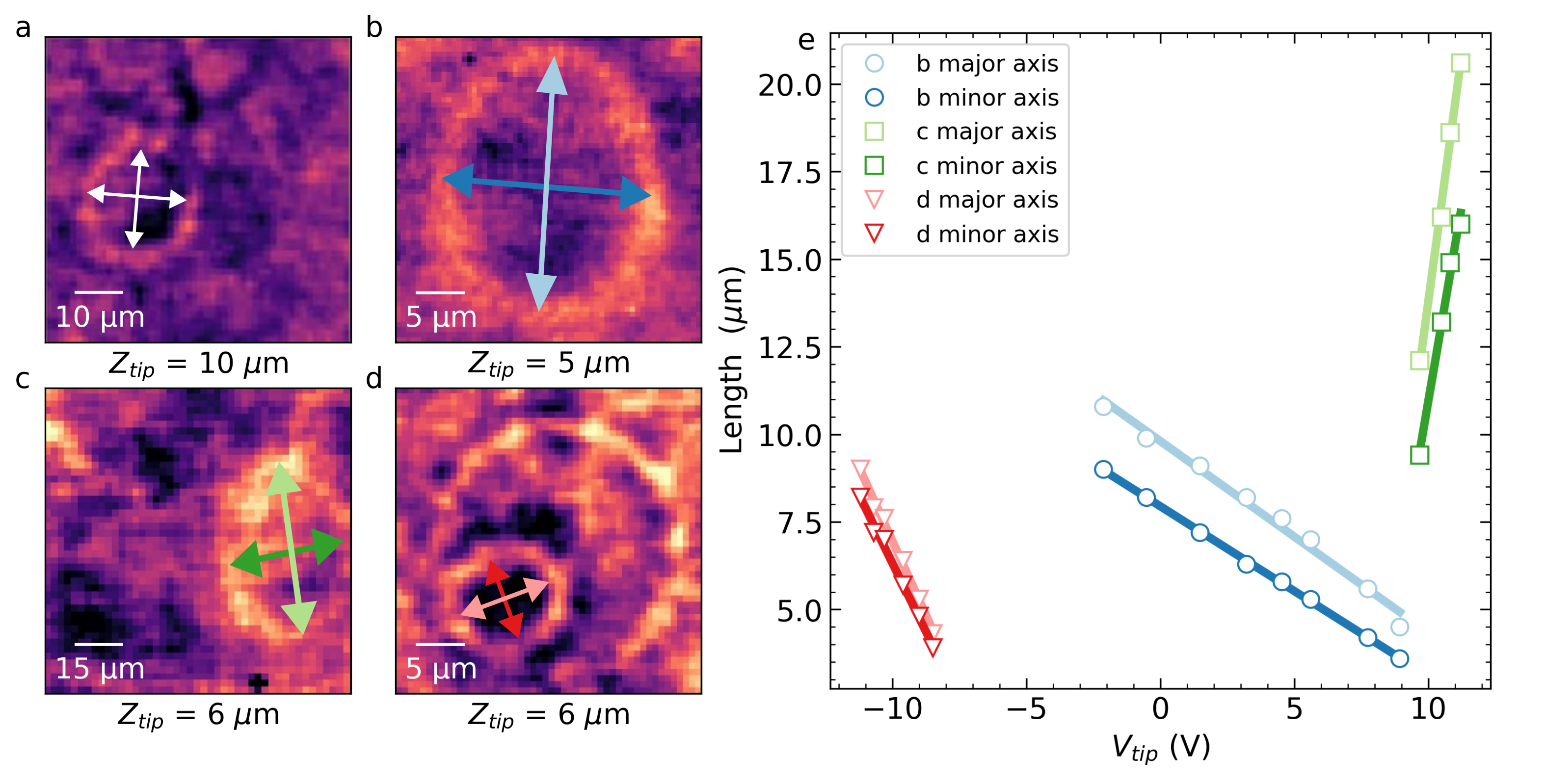
Zooming in closer to the defect manifesting as the ring in Fig. 2 and bringing the tip closer to the sample surface results in the images in Fig. 3a and 3b with and respectively. Notably, when the tip is closer to the surface, the shape transforms from a circular to an elongated contour, which fits well to an ellipse. The major and minor axes of the fitted ellipse both shrink linearly with applied tip voltage as shown in Fig. 3e, and their ratio remains constant within experimental error. Zoomed-in images of a couple of other TLS defects that appear elliptic (located outside the field of view of Fig. 2) are shown in Fig. 3c and 3d for m. The in-plane orientations of all these ellipses differ and do not appear to correlate with any patterned device features. Instead, the elliptic shape is an indication of the TLS dipole moment orientation.
To extract this orientation, we proceed with modelling the expected response. Following Schuster et al. (2010), the transmission of the resonator when the tip voltage tunes a TLS to be resonant with it (i.e., for ) can be expressed as
| (2) |
where is the TLS linewidth and is the total resonator loss rate, given by the sum of the coupling and internal loss rates respectively. When the TLS-resonator coupling is weak ( kHz), the resonator response is mainly dissipative. In contrast, a large also induces shifts in the resonator frequency. Our simulations indicate that, experimentally, we more frequently encounter the former regime than the latter (an example of which is shown in Fig. 1f).
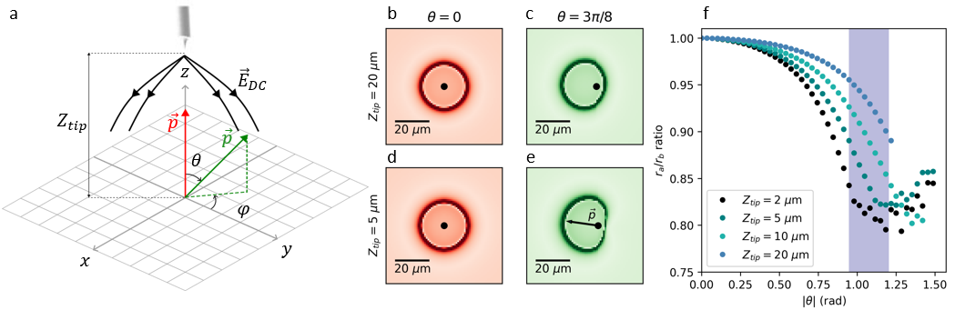
Information about the orientation of the TLS dipole moment is implicitly present in Eq. (2) via , defined in Eq. (1). Here the term implies that we can be selectively sensitive to the in-plane or out-of-plane component of by changing the direction of the applied electric field , enabled by a sharp tip. In Fig. 4a we define the TLS orientation by the in-plane () and out-of-plane () angles with respect to the tip coordinate system.
For a tip with a set voltage held at a particular height above the sample, the electric field distribution on the sample surface is computed in COMSOL. For a chosen orientation of the TLS dipole moment , the spatial data is then used to calculate from Eq. (2). In Fig. 4b, for illustration, we show such simulated TLS images for two different orientations of a TLS dipole moment for two different . This shows the expected circular contour for for both tip heights as the z-component of the electric field dominates in both cases. However, for large and small the in-plane component of the electric field becomes increasingly important, and an elliptical contour emerges. From this elliptical contour, the in-plane angle of the TLS dipole moment can be inferred directly from the angle of the short axis of the contour, meaning we can directly read from the panels in Fig. 3a-3d.
Deducing the polar angle requires more detailed simulations. We fit the simulated two-dimensional map (similar to images in Fig. 4c and 4e) to elliptical contours to extract the major () and minor () axes of the ellipses. The process is repeated as a function of and to obtain Fig. 4f. The plot shows that the change in from 10 to 5 m and resulting contour aspect ratio experimentally seen in Fig. 3a and 3b, corresponds to a narrow (shaded) range of possible for this TLS. Also noteworthy is that the smallest possible ratio obtainable is 0.8 for large , in good agreement with experimental observations as we have not seen any TLS with a smaller ratio. We note that in Fig. 4f, for very large , the ratio again starts to increase. This is due to the resonance contour starting to deviate from an elliptical shape.
The simulations indicate that for large the actual defect is located slightly off-center along the minor axis of the ellipse. Furthermore, they suggest that both the center of the ellipse and its aspect ratio change slightly with the applied tip voltage. Unfortunately, the large fields of view required to visualise these transitions are beyond the scan range of our microscope.
Although the slopes in Fig. 2h and 3e indicate the relative magnitudes of the TLS dipole moments, uncertainty in the exact electric field at the defect, and the unknown of each defect prevents extraction of . However, to reproduce the experimental results in our modelling, we assume eÅ Lisenfeld et al. (2019); de Graaf et al. (2018); Sarabi et al. (2016) which results in tip voltages very close to those used in our experiments. To precisely extract simultaneous frequency tuning of the device is required Lisenfeld et al. (2019).
Of the multitude of TLS present in the sample, our experimental setup is most sensitive to only those defects that are near the surface, close to the resonator and have stronger coupling to it. Thus, the observed TLS ought to be those most debilitating to device coherence.
Several factors can affect the shape of the observed contours. The width of the contour is related to the quality factor of the resonator, the linewidth of TLS, and . The spatial resolution is also limited by the sharpness of the AFM tip. Scanning electron microscope images of the tip, captured before and after the experiment (see Supplementary Information for details), demonstrate that the tip apex was never larger than a few microns during the six month experiment, setting our resolution. Out-of-plane tilting of the sample can also distort the contours. However, the tilt of the sample measured using AFM should result in a tip-sample height difference of only over a scan range, resulting in minimal distortion.
Another factor blurring the experimental images at small is the mechanical vibrations of the tip. Taking grid measurements with very small tip-sample distances were difficult, likely due to these mechanical vibrations in our system coming from the pulse tube cryocooler. In particular, attempting a grid over the defect in Fig. 3b at m resulted in the TLS ring disappearing also in subsequent scans at larger . We speculate this to be because of accidental contact with the defect, potentially also demonstrating the delicate glassy state of the TLS, susceptible to even minute perturbations. More stable scanning will allow closer imaging and improved resolution down to 10’s of nm, ultimately limited by the achievable in-plane electric field gradient from the tip, set by the tip size.
Future experiments will undoubtedly have better control over these aspects, leading to a more precise determination of . Importantly, our simulations show that as long as the TLS defect is located a sufficiently large distance from any metalisation on the sample/device, the specific device geometry does not play a significant role. For TLS located very close to metallic structures on the sample, however, the electric fields will always be perpendicular to the metal, and hence these TLS will always appear as circular contours. It also means that the TLS observed here as ellipses are located on or in the dielectric substrate.
Several improvements to our experiment can yield significantly more information about the defects. For example, utilising a substrate back gate and applying an additional variable electric field in the vertical direction can pinpoint the location of defects in three dimensions. Recent studies have attributed the majority of decoherence in superconducting devices to surface losses Hung et al. (2024); Bilmes et al. (2020); Wenner et al. (2011), and a systematic study of TLS concentrations with height would be very beneficial to this discussion.
The bulk of our knowledge about TLS in superconducting quantum circuits is based on phenomenological models deduced from observing the behaviour of the devices they inhabit. Direct interrogation of individual defects is rare, and due to the complexity of the setup required, relatively little attention has been focused on understanding the physical and chemical nature of these defects. Our approach of combining scanning probe systems with live quantum circuit readout is a promising direction for further understanding decoherence mechanisms, and testing the validity of the standard tunneling model. Localising the defects using our technique will also facilitate their study using other established scanning probe and surface analysis techniques. Studying multiple devices and different fabrication techniques can help generate statistics on the concentration and origins of TLS in different materials. Such experimental approaches, coupled with atomistic modeling Holder et al. (2013); Wang et al. (2018); Un et al. (2022); Cyster et al. (2021) can aid in the understanding and eventual mitigation of TLS defects.
Acknowledgements
We thank A. Tzalenchuk and T. Lindstrom for helpful discussions. We acknowledge the support from the UK Department for Science, Innovation and Technology through the National Measurement System (NMS), the Engineering and Physical Sciences Research Council (EPSRC) (Grant Number EP/W027526/1), and Google Faculty research awards. S.K. and A.D. acknowledge the support from the Swedish Research Council (VR) (Grant Agreements No. 2019-05480 and No. 2020-04393).
References
- Berthier and Biroli (2011) L. Berthier and G. Biroli, Rev. Mod. Phys. 83, 587 (2011).
- Leggett and Vural (2013) A. J. Leggett and D. C. Vural, The Journal of Physical Chemistry B 117, 12966–12971 (2013).
- Anderson et al. (1972) P. W. Anderson, B. I. Halperin, and c. M. Varma, Philosophical Magazine 25, 1–9 (1972).
- Phillips (1972) W. A. Phillips, Journal of Low Temperature Physics 7, 351–360 (1972).
- Phillips (1987) W. A. Phillips, Rep. Prog. Phys. 50, 1657 (1987).
- Müller et al. (2019) C. Müller, J. H. Cole, and J. Lisenfeld, Rep. Prog. Phys. 82, 124501 (2019).
- de Graaf et al. (2022) S. E. de Graaf, S. Un, A. G. Shard, and T. Lindström, Materials for Quantum Technology 2, 032001 (2022).
- Klimov et al. (2018) P. V. Klimov, J. Kelly, Z. Chen, M. Neeley, A. Megrant, B. Burkett, R. Barends, K. Arya, B. Chiaro, Y. Chen, A. Dunsworth, A. Fowler, B. Foxen, C. Gidney, M. Giustina, R. Graff, T. Huang, E. Jeffrey, E. Lucero, J. Y. Mutus, O. Naaman, C. Neill, C. Quintana, P. Roushan, D. Sank, A. Vainsencher, J. Wenner, T. C. White, S. Boixo, R. Babbush, V. N. Smelyanskiy, H. Neven, and J. M. Martinis, Phys. Rev. Lett. 121, 090502 (2018).
- Mehmandoost and Dobrovitski (2024) M. Mehmandoost and V. V. Dobrovitski, Phys. Rev. Res. 6, 033175 (2024).
- Simmonds et al. (2004) R. W. Simmonds, K. M. Lang, D. A. Hite, S. Nam, D. P. Pappas, and J. M. Martinis, Phys. Rev. Lett. 93, 077003 (2004).
- Grabovskij et al. (2012) G. J. Grabovskij, T. Peichl, J. Lisenfeld, G. Weiss, and A. V. Ustinov, Science 338, 232 (2012).
- de Graaf et al. (2021) S. E. de Graaf, S. Mahashabde, S. E. Kubatkin, A. Y. Tzalenchuk, and A. V. Danilov, Phys. Rev. B 103, 174103 (2021).
- Lisenfeld et al. (2015) J. Lisenfeld, G. Grabovskij, C. Müller, J. H. Cole, G. Weiss, and A. V. Ustinov, Nature Communications 6, 6182 (2015).
- Bilmes et al. (2022) A. Bilmes, S. Volosheniuk, A. V. Ustinov, and J. Lisenfeld, npj Quantum Information 8, 24 (2022).
- Bilmes et al. (2020) A. Bilmes, A. Megrant, P. Klimov, G. Weiss, J. M. Martinis, A. V. Ustinov, and J. Lisenfeld, Scientific Reports 10, 3090 (2020).
- Bilmes et al. (2021) A. Bilmes, S. Volosheniuk, J. D. Brehm, A. V. Ustinov, and J. Lisenfeld, npj Quantum Information 7, 1 (2021).
- Lisenfeld et al. (2016) J. Lisenfeld, A. Bilmes, S. Matityahu, S. Zanker, M. Marthaler, M. Schechter, G. Sch¨on, A. Shnirman, G. Weiss, and A. V. Ustinov, Scientific Reports 6, 23786 (2016).
- Lisenfeld et al. (2019) J. Lisenfeld, A. Bilmes, A. Megrant, R. Barends, J. Kelly, P. Klimov, G. Weiss, J. M. Martinis, and A. V. Ustinov, npj Quantum Information 5, 105 (2019).
- Lang et al. (2004) K. M. Lang, D. A. Hite, R. W. Simmonds, R. McDermott, D. P. Pappas, and J. M. Martinis, Review of Scientific Instruments 75, 2726–2731 (2004).
- Geaney et al. (2019) S. Geaney, D. Cox, T. Hönigl-Decrinis, R. Shaikhaidarov, S. E. Kubatkin, T. Lindström, A. V. Danilov, and S. E. de Graaf, Scientific reports 9, 12539 (2019).
- de Graaf et al. (2013) S. E. de Graaf, A. V. Danilov, A. Adamyan, and S. E. Kubatkin, Rev. Sci. Instrum. 84, 023706 (2013).
- Zhang et al. (2024) P. Zhang, Y.-Y. Lyu, J. Lv, Z. Wei, S. Chen, C. Wang, H. Du, D. Li, Z. Wang, S. Hou, R. Su, H. Sun, Y. Du, L. Du, L. Gao, Y.-L. Wang, H. Wang, and P. Wu, “Ultra-broadband near-field josephson microwave microscopy,” (2024), arXiv:2401.12545 [physics.app-ph] .
- Oh et al. (2021) S. W. Oh, A. O. Denisov, P. Chen, and J. R. Petta, AIP Advances 11, 125122 (2021).
- Denisov et al. (2022) A. O. Denisov, S. W. Oh, G. Fuchs, A. R. Mills, P. Chen, C. R. Anderson, M. F. Gyure, A. W. Barnard, and J. R. Petta, Nano Letters 22, 4807 (2022).
- Marchiori et al. (2022) E. Marchiori, L. Ceccarelli, N. Rossi, G. Romagnoli, J. Herrmann, J.-C. Besse, S. Krinner, A. Wallraff, and M. Poggio, Applied Physics Letters 121, 052601 (2022).
- Mahashabde et al. (2020) S. Mahashabde, E. Otto, D. Montemurro, S. de Graaf, S. Kubatkin, and A. Danilov, Physical Review Applied 14, 044040 (2020).
- Ranjan et al. (2022) V. Ranjan, Y. Wen, A. K. V. Keyser, S. E. Kubatkin, A. V. Danilov, T. Lindström, P. Bertet, and S. E. de Graaf, Physical Review Letters 129, 180504 (2022), publisher: American Physical Society.
- Lindström et al. (2009) T. Lindström, J. E. Healey, M. S. Colclough, C. M. Muirhead, and A. Y. Tzalenchuk, Phys. Rev. B 80, 132501 (2009).
- de Graaf et al. (2020) S. E. de Graaf, L. Faoro, L. B. Ioffe, S. Mahashabde, J. J. Burnett, T. Lindström, S. E. Kubatkin, A. V. Danilov, and A. Y. Tzalenchuk, Science Advances 6, eabc5055 (2020).
- Schuster et al. (2010) D. I. Schuster, A. P. Sears, E. Ginossar, L. DiCarlo, L. Frunzio, J. J. L. Morton, H. Wu, G. A. D. Briggs, B. B. Buckley, D. D. Awschalom, and R. J. Schoelkopf, Phys. Rev. Lett. 105, 140501 (2010).
- de Graaf et al. (2018) S. E. de Graaf, L. Faoro, J. J. Burnett, A. A. Adamyan, S. E. Kubatkin, A. Y. Tzalenchuk, T. Lindström, and A. V. Danilov, Nature Communications 9, 1143 (2018).
- Sarabi et al. (2016) B. Sarabi, A. N. Ramanayaka, A. L. Burin, F. C. Wellstood, and K. D. Osborn, Phys. Rev. Lett. 116, 167002 (2016).
- Hung et al. (2024) C.-C. Hung, T. Kohler, and K. D. Osborn, Phys. Rev. Appl. 21, 044021 (2024).
- Wenner et al. (2011) J. Wenner, R. Barends, R. C. Bialczak, Y. Chen, J. Kelly, E. Lucero, M. Mariantoni, A. Megrant, P. J. J. O’Malley, D. Sank, A. Vainsencher, H. Wang, T. C. White, Y. Yin, J. Zhao, A. N. Cleland, and J. M. Martinis, Applied Physics Letters 99, 113513 (2011).
- Holder et al. (2013) A. M. Holder, K. D. Osborn, C. J. Lobb, and C. B. Musgrave, Phys. Rev. Lett. 111, 065901 (2013).
- Wang et al. (2018) Z. Wang, H. Wang, C. C. Yu, and R. Q. Wu, Phys. Rev. B 98, 020403 (2018).
- Un et al. (2022) S. Un, S. E. de Graaf, P. Bertet, S. E. Kubatkin, and A. V. Danilov, Science Advances 8, eabm6169 (2022).
- Cyster et al. (2021) M. Cyster, J. Smith, N. Vogt, G. Opletal, S. P. Russo, and J. H. Cole, npj Quantum Inf 7, 12 (2021).
SUPPLEMENTARY INFORMATION
I Superconducting resonator sample
The Nb on Sapphire resonator sample used in this work consists of a hanger-type resonator. It consist of two parallel prongs which serve as inductors, connected together on one side of the resonator. A series of interdigitated capacitors couple the two prongs to each other. The interdigitated capacitors concentrate the electric fields inside the resonator, thereby enabling stronger coupling to TLS, facilitating easier detection. The two prongs are connected to the ground plane on either side of the resonator (through an inductive filter, seen in the scan of Fig. 1c), to facilitate the application of a DC current through the resonator. This can be used to tune the resonance frequency, a property not utilised in this work.
The fundamental mode of the resonator results in the microwave voltage standing wave amplitude as sketched in Fig. 1b. The inductive filters are located in the voltage node to maximise the quality factor of the resonator. In this region the sensitivity to TLS is reduced as here they couple weakly to the resonator microwave field. Instead we detect the TLS most detrimental to device performance near the voltage anti-nodes.
II Experimental microwave setup
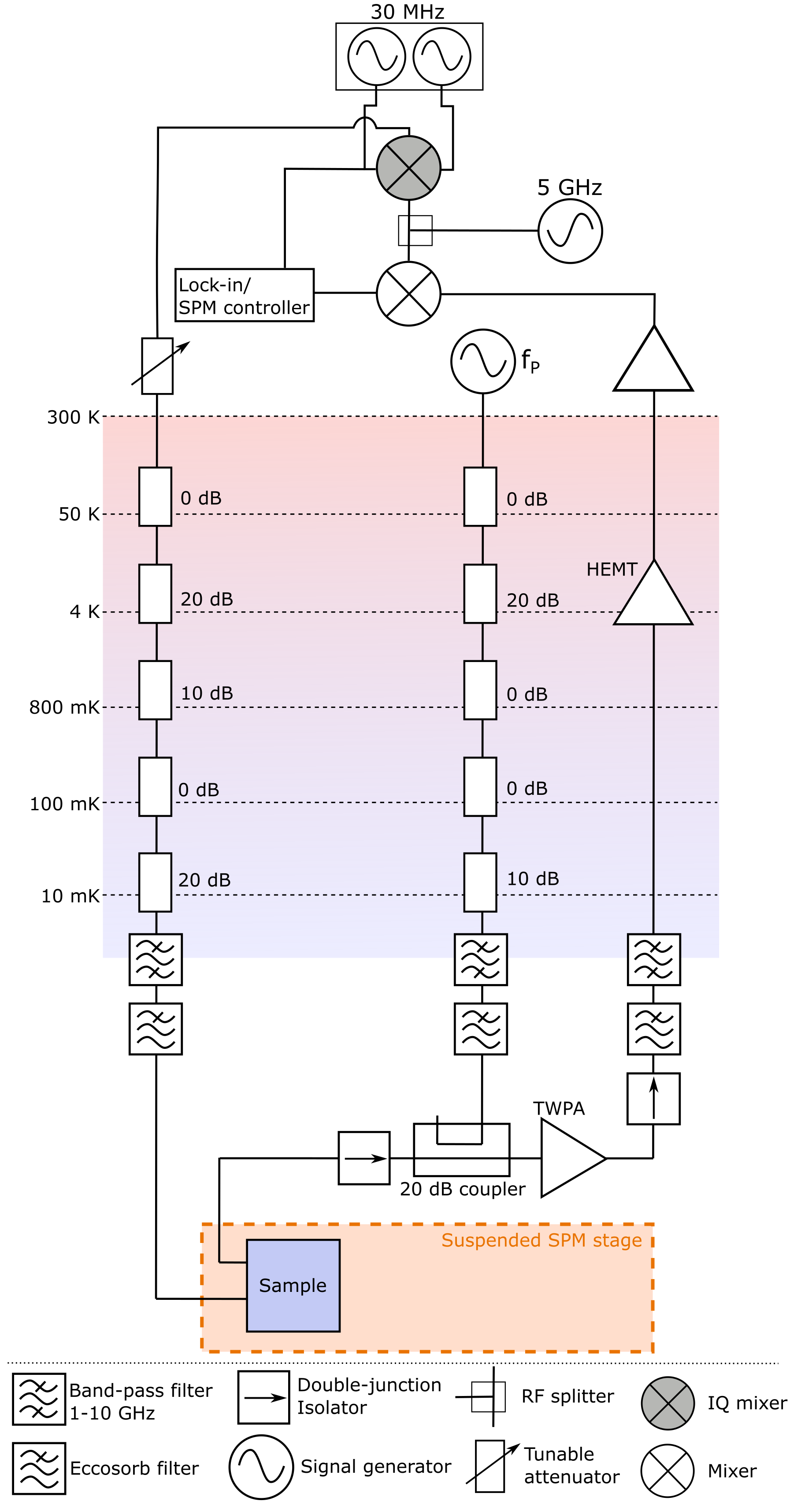
Supplementary Fig. 1 shows the configuration of the microwave wiring inside the dilution refrigerator, and the setup of the heterodyne detection scheme at room temperature. In brief, two low-frequency (30 MHz) phase-shifted signals are up-converted to a single side-band tone at the sample resonance frequency, and passed down a heavily attenuated coaxial line to the sample on the SPM stage. The signal from the sample is then returned via a travelling-wave parametric amplifier (TWPA, SilentWaves Argo; driven by a pump tone at GHz) before being further amplified by a high-electron mobility transistor (HEMT) amplifier at the 4K stage of the cryostat, and further amplified at room temperature to the desired level. The signal is then again down-converted to 30 MHz and demodulated using a lockin-amplifier, which feeds the two analog demodulated quadrature signals, proportional to the microwave transmission at the chosen frequency , to the SPM control electronics (Nanonis). We record the data from both quadratures, but rotate the phase such as to put most of the signal in one of the quadratures. For simplicity, the data shown in the manuscript is from one of these quadratures only.
III SEM images of the tip
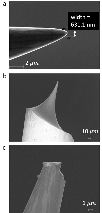
The tip used for AFM and applying the local gate voltage was produced by etching a 0.25 mm tungsten wire in a KNO solution. The etched tip was cleaned in deionised water to both stop the etching process and clean any residual salts sticking to it. The tip was then imaged using SEM to verify its sharpness. An SEM image of the tip taken before scanning is shown in Supplementary Fig. 2a.
Images taken after scanning for six months (Supplementary Fig. 2 b and c) show that it became blunt over time. Nevertheless, the end diameter was still less than . The simulation results presented in this work used a tip with a diameter of to accurately model our observations.
IV TLS saturation and power dependence
A common signature of TLS is through their power dependence. At low microwave powers, TLS can absorb photons from the resonator, making TLS the primary source of loss in the circuit. At higher microwave powers, TLS cannot dissipate the absorbed energy as phonons quickly enough, causing them to saturate. In Supplementary Fig. 3 we show the power dependence of the internal and external (coupling) quality factors of the resonator in which TLS were imaged in this work.
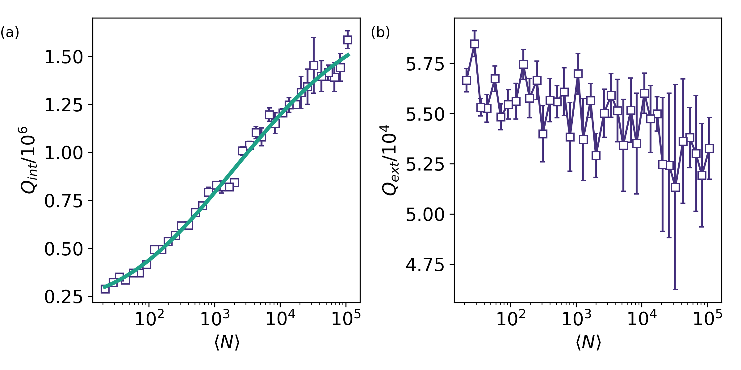
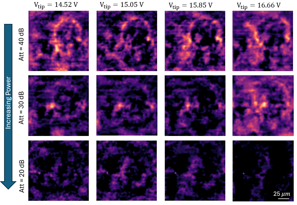
We estimate the average photon number by , where is the total and the external (coupling) quality factors obtained from fits to the VNA data, and is the microwave power reaching the sample. In Fig. 3 we show the internal and external quality factor as a function of . The data is fitted to , finding , critical photon number , TLS limited loss and power-independent loss of . The quoted error bounds include propagated errors from the data. This strong dependence of on power indicates that the quality factor is strongly limited by TLS, which are saturated at increased driving powers.
We further confirm TLS saturation by imaging individual TLS in our SGM setup. This is shown in Supplementary Fig. 4. For our experiments, we found that an average photon number in the range of provides a good compromise between TLS sensitivity and signal-to-noise ratio.
Supplementary Fig. 4, shows grids taken at the exact same location at different driving powers, by adjusting the variable attenuator on the signal input line shown in Supplementary Fig. 1. From each panel, a background has been subtracted and all are plotted in the same colour scale. At low powers (high attenuation, top panels), we see a ring that grows with increasing tip voltage. The fluctuations reduce and ultimately disappear as the driving power is increased (bottom panels), showing that this individual TLS is saturated.
V Electrostatics modelling
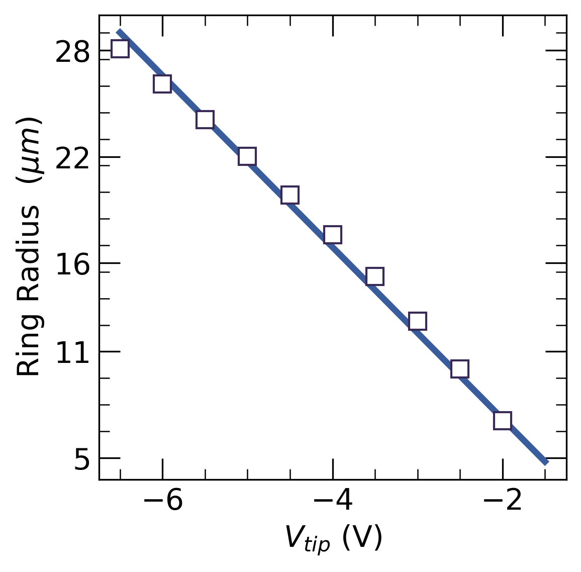
To simulate the frequency shift of a TLS and the resultant change in the transmission as it becomes resonant with the resonator, a simplified tip and sample geometry was simulated. In particular, a conical tip with a hemispherical bottom was chosen for the tip geometry (Supplementary Fig. 5). The dimensions of the tip were chosen to be comparable to that of the actual tip dimensions, as measured by SEM imaging (in Supplementary Fig. 2). A square m wide and m thick substrate slab of sapphire under the tip imitated the sample. The underside of the sapphire slab was grounded and the tip was held at a potential of 1 V. While this is a significant oversimplification of the sample geometry, the agreement between experimental and simulated results shows that our technique is able to capture the TLS dipole orientation even in the simplest of scenarios. A number of unknown experimental parameters (e.g. exact tip size and shape, exact local electric field strength, TLS location within the substrate/surface) will influence the exact determination of . Future studies will undoubtedly have increased knowledge of these parameters.
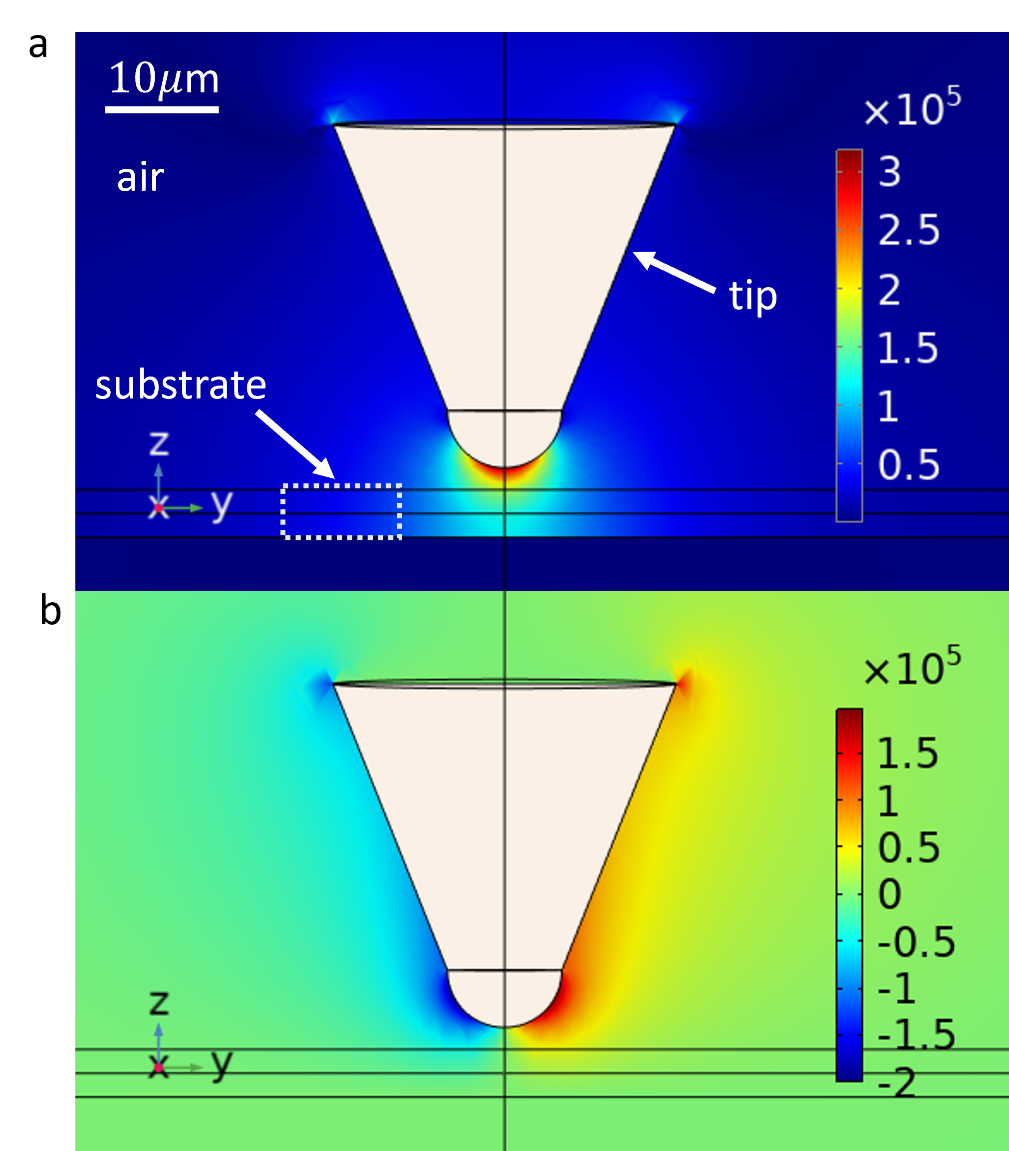
Supplementary Fig. 5 shows the magnitude of the simulated electric fields in the vertical () and horizontal () directions around the tip.
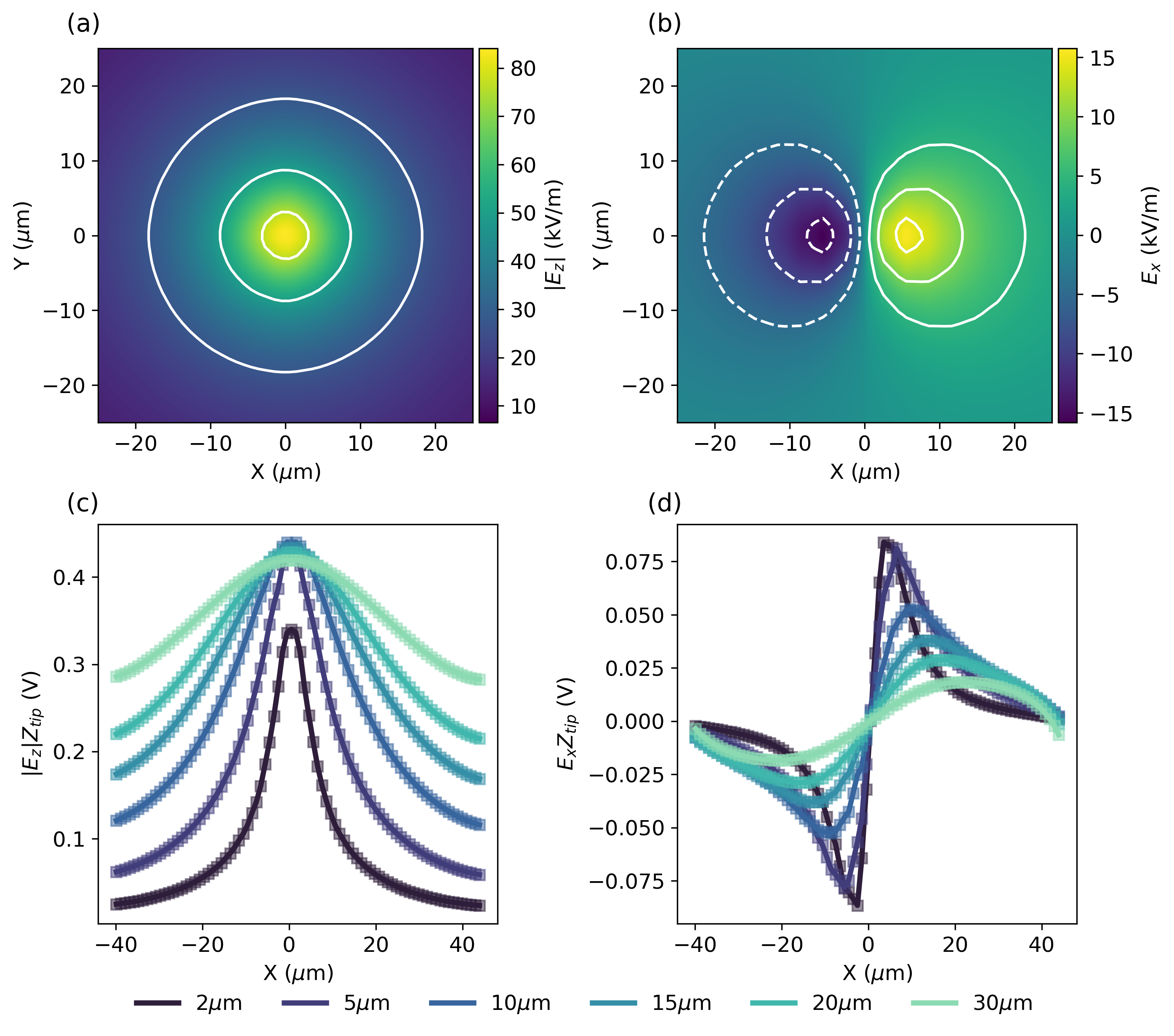
Similarly, Supplementary Fig. 6 (a-b) shows the resulting electric field strength in the sample plane, separated into the Z and X components respectively.
Supplementary Fig. 6 (c-d) compares the same electric field strengths as in Supplementary Fig. 6 (a-b) at for different tip-sample separations for (c) and (d) . Here we have scaled the data by the expected scaling. For we see that this almost collapses the curves at (some deviation due to finite tip size), and the larger results in a more delocalised electric field distribution, as expected. In Supplementary Fig. 6d we show the behaviour of with the same scaling applied. Here we see similar broadening, and we also see that the lateral component of the electric field vanishes much faster with increased tip-sample distance. I.e. ellipses could only be observed for small .
To mimic the change in voltage on the tip in the experiment we multiply the resulting with a prefactor, before calculating the measured signal quantity through Eq. (2). Varying the tip voltage in simulation reproduces the change in size of the rings. As an example, in Supplementary Fig. 7 we plot the ring radius as a function of tip voltage, using parameters for the TLS resulting in a ring similar to that in Fig. 2 of the main text. Also, in simulations the ring radius shrinks approximately linearly with applied tip voltage, in analogy with Fig. 2h.