Study of non-diffusive thermal behaviors in nanoscale transistors under different heating strategies
Abstract
Understanding the phonon transport mechanisms and efficiently capturing the spatiotemporal distributions of temperature is of great significance for alleviating hotspot issues in the electronic devices. Most previous simulations mainly focused on the steady-state problem with continuous heating, and the effective Fourier’s law (EFL) is widely used for practical multiscale thermal engineering due to its simplicity and efficiency although it still follows the diffusive rule. However, non-continuous heating is more common in the electronic devices, and few comparative study is conducted to estimate how much deviation the EFL would produce. To answer above questions, the heat conduction in nanoscale bulk or silicon-on-insulator (SOI) transistors is investigated by the phonon Boltzmann transport equation (BTE) under three heating strategies, namely, ‘Continuous’, ‘Intermittent’ and ‘Alternating’ heating. Numerical results in the quasi-2D or 3D hotspot systems show that it is not easy to accurately capture the micro/nano scale heat conduction by the EFL, especially near the hotspot regions. Different heating strategies have great influence on the temperature rise and transient thermal dissipation process. Compared to ‘Intermittent’ heating, the temperature variance of ‘Alternating’ heating is smaller.
keywords:
Micro/nano scale heat conduction , Hotspot issues , Transistors , Boltzmann transport equation , Effective Fourier’s law1 INTRODUCTION
With the vigorous development of aerospace, artificial intelligence, microelectronics or semiconductors, new energy vehicles and other advanced technologies, the geometric size of transistors represented by MOSFET and FinFET decreases sharply from microns to nanometers [1], package density increases, thermal power density increases sharply, and hotspot issues begin to seriously threaten the performance and safe operation of devices [2, 3, 4, 5, 6, 7]. Due to the high cost of updating inspection and experimental testing of industrial products, numerical thermal simulations dominated by industrial software such as TCAD, ANSYS and COMOSL, play a key role in every link of industrial production [2, 7]. Computational efficiency and accuracy have become two key elements and challenges in the engineering thermal simulations [8, 9, 2, 10, 11, 12].
As we all known, the macroscopic method is widely used in practical multiscale thermal engineering because its computational efficiency is much higher than that of mesoscopic or microscopic methods. Although a lot of experiments over the past decades have shown that the classical Fourier’s law with bulk thermal conductivity significantly underestimates the temperature rise in nanoscale transistors because the thermal conductivity of the materials at the micro/nano scale is not a constant but decreases with size [13, 14, 15, 16], its diffusion form is still retained and widely adopted, namely, the linear relationship between the heat flux and temperature gradient. For example, the Effective Fourier’s law (EFL) is widely used by engineers and integrated into industrial softwares [17, 2, 18],
| (1) |
The only difference from the classical Fourier’s law is that the position- or size- dependent effective thermal conductivity is introduced instead of the bulk thermal conductivity. Actually the selection of the effective thermal conductivity coefficient is very dependent on the experience of the engineers, and improper selection will lead to huge deviations. Apart from the EFL, many macroscopic thermal models or moment equations [19, 20, 21, 22] have also been developed based on Chapman-Enskog, Hermite expansions or data-driven machine learning [23], in which nonlinear, nonlocal terms are introduced to replace the linear assumption between the heat flux and temperature gradient.
Although macroscopic models have made great success in multiscale thermal analysis, its scope of application and accuracy still suffer from great challenge, especially when the system size [13], spacing of heat source [24, 25, 14, 26, 15] or heating period [27, 28] is getting smaller, and the materials components and geometric design are getting more complex. With current computing power, it is still impractical to use microscopic methods to simulate the heat dissipation of chips or electronic devices but it is accessible to numerically solve the phonon Boltzmann transport equation (BTE) [9, 2, 29, 30, 10, 11], which describes the physical evolutions of the phonon distribution function in the momentum, position and time space instead of temperature diffusion.
In fact, the multi-scale thermal simulation method with BTE as the core bridge and connected with microscopic or mesoscopic methods has been greatly developed in the semiconductor top enterprises [31, 18] or research centers. For instance, the IMEC research team [32, 33] used the modular method to evaluate the thermal performance of the back-end of line (BEOL). They calculated the thermal physical parameters of electrons and phonons using the first principles as the input parameters of BTE, and then used the Monte Carlo method to numerically solve the BTE and extracted the effective thermal conductivity of materials such as nanoscale interconnects and through-holes. Finally, the EFL is solved to extract the effective thermal resistance of each layer of BEOL in a reasonable calculation time. The Intel research team [2, 18] numerically solves the phonon BTE to obtain the effective thermal conductivity of the entire silicon fin or nanowires, where the heat source term is obtained from electron-phonon coupling. After that, a larger thermal simulations at the cell or circuit level is conducted to assess the effects of self-heating on interconnects and circuits by numerically solving the EFL.
Above studies show that mesoscopic methods begin to play an important role in engineering multiscale thermal simulation with the improvement of computing power, and can extract the required macroscopic effective coefficients for macroscopic models and make calibration corrections. However, few comparative studies are conducted to estimate how much deviation the EFL would produce compared to the phonon BTE. In addition, a continuous heating source is usually used in the previous studies of heat dissipation in transistors [34, 35, 36, 37, 18, 33, 38] and researchers mainly focus on the steady-state temperature field. Actually the electronic equipments do not always work and the transient thermal evolution process is also noteworthy [39, 2, 25].
In this work, we try to investigate the effects of heat source on thermal conduction in hotspot systems. We adopt various heating strategies and the associated steady or unsteady thermal dissipations processes are simulated, analyzed and discussed. And a comparative study is conducted between the predictions of phonon BTE and EFL for the heat dissipations in hotspot systems. The rest of this article is organized as follows. Theoretical models and methods are introduced briefly in Sec. 2. Results and discussions for the heat dissipation in quasi-2D and 3D hotspot systems are conducted in Sec. 3. Finally, conclusion and outlook are made in Sec. 4.
2 MODELS AND METHODS
To capture the transient heat dissipations in electronic devices [2, 18, 40] which is mainly composed of three-dimensional semi-conductor materials, the phonon BTE under the single-mode relaxation time approximation (RTA) is used [41, 8, 9, 29, 30, 10, 11],
| (2) |
where is the phonon distribution function of energy density, which depends on spatial position , unit directional vector and time . is the associated equilibrium distribution function, is the phonon group velocity and is the external heat source. Taking an integral of Eq. (2) over the solid angle space leading to the first law of thermodynamics with energy and heat flux ,
| (3) | |||
| (4) |
where is the specific heat and is the temperature.
BTE describes the evolution of the phonon distribution function in the multi-dimensional phase space, where a large number of phonon migrations happen simultaneously with phonon scattering. The average time experienced between two adjacent phonon scatterings is the relaxation time and the corresponding average distance is the mean free path . Compared to the macroscopic models, the phonon BTE has a higher degree of freedom, which increases computational cost but improves accuracy. Compared to full scattering kernel, the complex interactions between different phonon modes or other energy carriers [42, 43, 44, 45, 36] are ignored in the RTA-BTE, which loses accuracy but greatly improve computational efficiency. The two main three-dimensional semiconductor materials that make up transistors are silicon and silicon dioxide, whose thermal properties at room temperature K are listed in Table. 1. Actually the phonon Umklapp scattering process dominates the heat conduction and the normal scattering process can be ignored in conventional three-dimensional semiconductor materials, so that the RTA-BTE model is sufficient to describe the phonon heat conduction problem in electronic devices [29, 30, 10, 11, 18, 40]. In addition, the isotropic wave vector and frequency-independence assumption is used in the present model to achieve a good balance between computational efficiency and accuracy. The present model can correctly capture some nonlinear, nonlocal and ballistic effects, and be in consistent with experiments for the heat conduction in room temperature semi-conductor materials [9, 15, 46]. If there is a more accurate and efficient model in the future, we are happy to adopt it for practical multiscale thermal engineering.
| (J mK-1) | (ms-1) | (nm) | (W mK-1) | |
|---|---|---|---|---|
| Si | 1.5E6 | 3.0E3 | 100.0 | 150.0 |
| SiO2 | 1.75E6 | 5.9E3 | 0.4 | 1.4 |
The interfacial thermal resistance between two dissimilar solid materials is [49, 50]
| (5) |
where and are the temperature drop between the two sides of the interface and the heat flux across the interface, respectively. In order to deal with the interfacial thermal resistance between silicon and silicon dioxide materials, the diffuse mismatch model is used [50, 49, 51, 17], which assumes that all phonons loses previous memories and completely follows the diffuse transmitting or reflecting rule after interacting with the interface. Transmittance and reflectance on each side of the interface satisfy
| (6) |
due to energy conservation, where (or ) represents the transmittance from medium (or medium ) to medium (or medium ) across the interface, and (or ) represents the reflectance in the medium (or medium ) reflected back from the interface. Note that the net heat flux across the interface should be zero at the thermal equilibrium state due to the principle of detailed balance so that
| (7) |
where and (or and ) are the specific heat and group velocity of medium (or medium ).
Discrete unified gas kinetic scheme (DUGKS) is used to solve the transient frequency-independent phonon BTE. More specific numerical solution process and boundary treatments can be found in previous papers [41, 52]. Here we make a brief introduction of DUGKS. Under the discretized six-dimensional phase space, the phonon BTE is
| (8) |
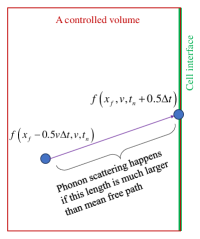
where , , , are the indexes of cell center, solid angle, cell interface and time step at the finite-volume discrete level, respectively. . In order to update the phonon distribution function from to , the key is the reconstruction of the distribution function at the cell interface at the half time step . When a phonon is transferred from the inner region of a control volume to the interface after half a time step, it will suffer a large number of phonon scattering processes if the time step is much longer than the phonon relaxation time or this length is much larger than mean free path, as shown in Fig. 1(a). To respect this physical law, the phonon BTE is solved again along the direction of group velocity and trapezoidal quadrature is used for the time integration of the scattering terms,
| (9) | ||||
| (10) |
where is the center of cell interface, , , . Equations (8) and (9) are the key evolution process of DUGKS [41], that is, solving the discrete BTE at the cell center in a complete time step, while coupling phonon advection and scattering together in the reconstruction of the interfacial distribution function at the half time step, through which it allows the time step or cell size to be much larger than the relaxation time and phonon mean free path in the (near) diffusive regime. The phonon distribution function incident into the cell interface is
| (11) |
from which it can be found that we have to firstly calculate the equilibrium state at the cell interface if we want to reconstruct the distribution function based on .
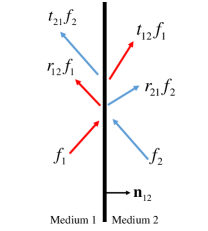
Here we focus on how to reconstruct the transmission and reflection distribution function at the interface between two dissimilar solid materials. As shown in Fig. 1(b), the phonon transmission and reflection at the interface are related to the phonon distribution on both sides. Diffuse mismatch model assumes that the phonon distribution at the interface pointing from interface to medium (or medium ) follows the equilibrium distribution with temperature (or ). Then we have
| (12) | ||||
| (13) | ||||
| (14) | ||||
| (15) | ||||
| (16) | ||||
| (17) |
where is the unit normal vector pointing from media to media , and are the local equivalent equilibrium temperatures on each side of the interface. (or ) and (or ) are the phonon properties in medium (or medium ). The first two equations (12,13) come from the physical assumptions of diffuse mismatch model and the conservation of heat flux across the interface, for example, in Eq. (12), all phonons in medium emitted from the interface, including the phonons in medium reflecting back from the interface and the phonons in medium transmitting across the interface, follow the equilibrium distribution with temperature . (14) and (15) are calculated by taking the moment of distribution function over the whole momentum space. Combined above six equations, , , and can be obtained by Newton method.
3 RESULTS AND DISCUSSIONS
In this section, the steady/unsteady heat dissipation in nanoscale bulk or SOI transistors under different heating strategies is simulated and discussed by numerically solving the phonon BTE. A comparative study is conducted between the predictions of phonon BTE and EFL to estimate how much deviation the EFL produces. Detailed numerical solutions of EFL can be found in A as well as the specific values of effective thermal conductivity.
3.1 Quasi-2D hotspot system
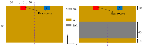
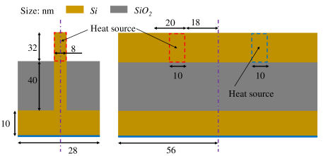
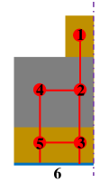
Heat conduction in quasi-2D hotspot system is simulated, as shown in Fig. 2(a), where nanoscale heat sources are embedded in the silicon substrate. All geometric sizes are shown in the pictures and two geometries are simulated. One is bulk structure composed of silicon and the other is SOI structure composed of silicon and silicon dioxide materials. The left and right sides of this geometric structure are symmetric boundaries. The top is adiabatic diffusely reflecting boundary conditions with zero heat flux, and the bottom is the heat sink with fixed environment temperature and treated with isothermal boundary conditions. The whole structure is like the MOSFET devices with Joule heat generation and dissipations [37, 48].
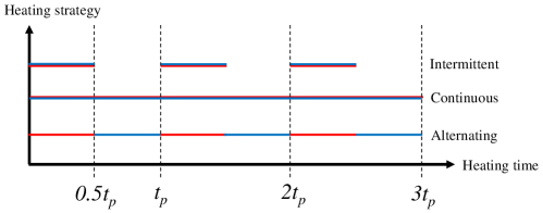
Three different heating strategies are mainly considered, as shown in Fig. 2(b), where ‘Continuous’ represents that the two external heat sources always heat the system. It indicates a steady heat source, which is used in most previous papers. ‘Intermittent’ represents that the two external heat sources work together and both of them heat the system in a half time. It is a bit like the heating method in TDTR experiments, where the heat source heats the system for a while and does not heat it for a while. ‘Alternating’ represents that the two external heat sources work alternatively and each one heats the system in a half time, where is a heating period. It is much like the N and P type transistors in chips are periodically arranged on the substrate and interlace to work when the AC voltage is loaded. For typical chips in electronic devices (e.g., laptop), the working frequency is about GHz so that we set ns. The maximum heating power is Wm-3.
Phonon mean free path of room temperature silicon is nm (1), a bit larger than the system length or height, which indicates that classical Fourier’s law is no longer valid. While the phonon mean free path of silicon dioxide is nm, much smaller than system size. In other words, the heat conduction in silicon is far from the diffusive regime and closer to ballistic regime while the phonons in silicon dioxide follows the diffusive transport. In order to better show the difference between diffusive and ballistic transport, we also make a comparison between the results predicted by EFL where the effects of boundary scattering are reflected in the effective thermal conductivity (28).
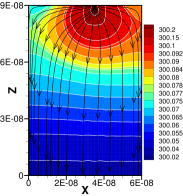
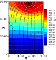
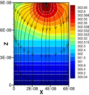
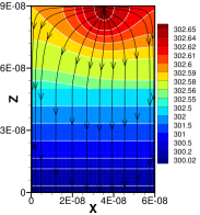
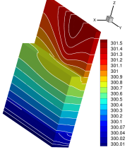
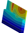
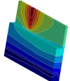
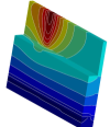
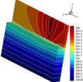
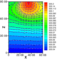
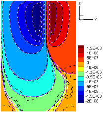
The steady temperature fields are simulated and shown in Fig. 3, where detailed numerical discretizations and independence test can be found in B. Firstly, it can be found that the peak temperature rise predicted by EFL is smaller than that predicted by BTE although a smaller effective thermal conductivity is used instead of bulk thermal conductivity. One reason is that the effects of boundaries scattering on phonon transport in this geometry are various in different spatial boundary regions rather than a simple effective boundary scattering rate. Boundary scattering leads to a thermal resistance or temperature slip near the boundaries which is ignored in the EFL, which can be found from Fig. 3(c,f). And the other reason is the linear relationship between the heat flux and temperature, which may be no longer valid in some spatial regions. For example, phonons emitted from the heat source areas transport freely and follow the ballistic rule with group velocity before scattering with boundaries or other phonons. Hence, the temperature contour lines near the hotspot are similar to the rectangle geometry of heat source, as shown in Fig. 3(a)(d). But the results predicted by EFL are like a circle due to temperature diffusion, as shown in Fig. 3(b)(e). It can also be observed that in the left or right top corners, the temperature distributions are sharp, not smooth, and there is heat flux flowing from the low temperature to high temperature, which exactly breaks the diffusive rule. This could be explained that the phonons transport from the heat source areas to the left or top corner boundaries and the phonons diffusely or specularly reflected from the boundaries stack together, which results in a back-flow of heat flux.
Secondly, compared to the heat conduction in bulk structure, the existence of silicon dioxide in SOI structure increases the peak temperature rise due to its smaller thermal conductivity or diffusivity. Diffusive transport dominates heat conduction in silicon dioxide region so that its temperature distributions are linear and similar to those predicted by EFL, as shown in Fig. 3(d,e,f). Besides, there are phonon diffusely reflecting and transmitting in the Si/SiO2 interfaces, which shorten the phonon mean free path similar to the boundary scattering. It can be found that there are temperature jump between the Si/SiO2 interface and the thermal dissipation is blocked by the large thermal resistance if making a comparison of temperature fields between Fig. 3(a,d), (b,e) or (c,f).
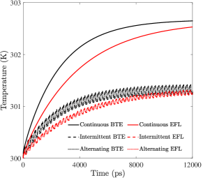
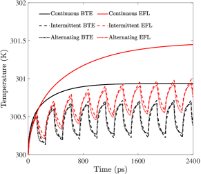
Thirdly, the evolutions of transient peak temperature rise under three different heating strategies are shown in Fig. 4. After phonons absorb thermal energy from the heat source, they will transfer it to other phonons or spatial regions. Ballistic transport dominates this process near the nanoscale heat source regions due to the smaller sizes, so that the thermal energy absorbed from heat source is dissipated to other spatial regions with rare scatterings or low thermal resistances. Hence, this energy exchange and transfer process is very efficient. On the contrary, it follows the diffusive rule in the EFL with a reduced effective thermal conductivity by boundary scattering, which significantly reduces the heat dissipations efficiency. Therefore, it can be found that when the heat source is removed, the temperature drop predicted by BTE is larger than that predicted by EFL.
The temperature distributions reach periodic steady state after heating period in bulk structures, that is, the temperature variance in the next heating period is the same as the temperature distribution in the current heating period. However, it needs heating period to reach periodic steady state in SOI structures. For ‘Intermittent’ heating, both two heat source heat the system together so that it could reach a higher peak temperature. But when the two heat source are both removed, the temperature drop is large. For ‘Alternating’ heating, the two heat source heat the system in turn. The distance between two heat source is smaller than the phonon mean free path, which indicates that the phonons emitted from one heat source can efficiently affect the other heat source in one heating period. Hence, compared to ‘Intermittent’ heating, its peak temperature rise is smaller, but its temperature drop is smaller, too. In addition, it can be found that the peak temperature becomes a constant in one heating period. This is because when one heat source is removed, its neighboring heat sources begin to provide heat energy, and the thermal energy provided by the neighboring heat sources is equal to the rate of heat dissipation. Compare to ‘Intermittent’ heating, the temperature variance of ‘Alternating’ heating is smaller, which indicates that this heating strategy has less thermal shock on the material.
3.2 3D hotspot system
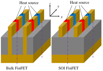
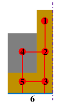
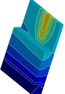
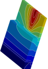
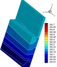
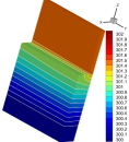
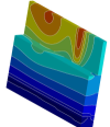
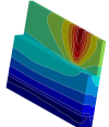
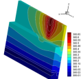
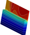
In order to get closer to the thermal physical process of actual 3D semi-conductor devices [5], the transient heat conduction in 3D hotspot systems including the bulk or SOI FinFET is investigated. It is worth noting that the heat transfer process in actual chip structure is complex, consisting of billions of transistors and tens of materials and involving multi-scale and multi-physical coupling, which are very challenging to simulate. This study mainly refers to many examples in the past literature [38, 44, 18, 5, 36], and only investigates the transient phonon conduction problem in single or several transistors. Schematics of bulk or SOI FinFETs are shown in Fig. 5, both of which are composed of silicon fin, silicon dioxide insulation layer and silicon substrate with several contact interfaces. The system sizes in the , , direction of a single FinFET are nm, nm and nm, respectively, which is comparable to the phonon mean free path of silicon and much larger than that of silicon dioxide. Front, back, left and right surfaces are all symmetric boundaries. The whole diagram is geometrically symmetric in the and directions with respect to the purple dot dash lines. Bottom surfaces are the heat sink with fixed environment temperature and the other surfaces are all diffusely reflecting adiabatic boundaries. The heat source is located in the fin area, whose system size in the , , direction are , and nm, respectively. More detailed geometry sizes can be found in Fig. 5(b) and the entire structure size is approximately a nm technology node transistor. We adopt the same heating strategies, frequency and power as used in Fig. 2(b) and Sec. 3.1.
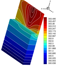
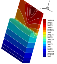
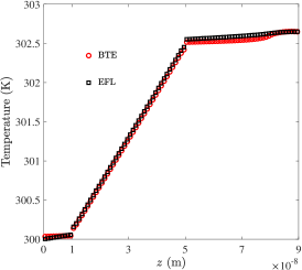
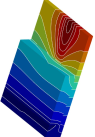
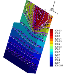
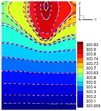
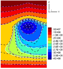
Steady temperature fields of bulk or SOI FinFET are shown in Fig. 6, where detailed numerical discretizations and independence test can be found in B. A comparison is made between the results predicted by phonon BTE and EFL and only a half of FinFET is plotted due to symmetry. It is found that the peak temperature rise predicted by the EFL is higher than that of phonon BTE, which is opposite to the results in the quasi-2D hotspot system shown in Fig. 3. Actually these opposite results reflect the contingency and experience of practical engineering thermal simulation. It is well known that the EFL is widely used in the practical engineering thermal simulation and the choice of effective thermal conductivity is significantly related to the experience of the engineers. The current results (Figs. 3 and 6), in which the temperature rise predicted by EFL is sometimes lower than BTE and sometimes higher than BTE, reflect that the experience of engineers is critical to the accuracy of the results because a lower effective thermal conductivity obviously will result in a higher temperature rise.
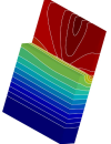
It can also be found that the deviations of temperature fields in the whole domain between the BTE and EFL are smaller in SOI FinFET that those in bulk FinFET. This is actually related to the compositions of the material and the characteristics of phonon transport. Schematic of heat dissipation or phonon transport paths in bulk FinFET and SOI FinFET are shown in Fig. 6(c) and (f), respectively, where there is thermal resistance in the channels between two nodes. When phonons need to transport thermal energy from the heat source region to the heat sink region, they must pass through two Si/SiO2 interfaces and the silicon dioxide region in SOI FinFET, as shown in Fig. 6(f). On one hand, the small phonon mean free path in silicon dioxide leads to a diffusive transport, where the EFL is exactly valid. On the other hand, two Si/SiO2 interfaces significantly increases the thermal resistance and decreases the heat dissipation efficiency. As can be seen from Fig. 6(d,e), the temperature gradient is basically only along the direction and the temperature variance presents a linear distribution in the silicon dioxide and bottom silicon substrate areas. However, after phonons absorb a large amount of energy from the heat source, they can transfer energy directly from the heat source region to the bottom heat sink only through the silicon material in the bulk FinFET, namely, heat dissipation path in Fig. 6(c), just like the heat conduction in a quasi-2D system. In this process, ballistic transport dominates the heat conduction. Although a lower effective thermal conductivity is introduced in the EFL, the linear assumption between the heat flux and temperature gradient still leads to some deviations compared to the results of phonon BTE, which has also been verified in the last section, i.e., Fig. 3.
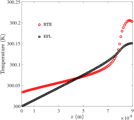
The temperature fields in bulk FinFET predicted by phonon BTE in the bottom silicon substrate areas (Fig. 6a) are completely different from those predicted by EFL (Fig. 6b). Actually it is a competition result of two heat dissipation channels with different heat transfer efficiency and various phonon transport behaviors, which can be explained according to the heat dissipation channel and in Fig. 6(c). In heat dissipation channel , the transfer of thermal energy only happens in the silicon materials without interfacial thermal resistance and ballistic phonon transport dominates heat conduction. The only thing that might affect the efficiency of heat conduction is the smallest system characteristic length, which changes from nm to nm. While in heat dissipation channel , on one hand, two interfacial thermal resistance exists in the thermal transport process from to and from to . One the other hand, the phonon mean free path of silicon dioxide is much smaller than nm. In other word, there is bigger thermal resistance and lower phonon transport efficiency in channel , which indicates that the phonon transport efficiency or the speed of heat conduction is slower than that of channel under the framework of phonon BTE. Hence, it can be found that the temperature contour line in bottom silicon areas is even perpendicular to the bottom surface. However, ballistic phonon transport in heat dissipation channel is replaced by the temperature diffusion with the effective thermal conductivity in the EFL. In other words, there are only temperature diffusion with spatial dependent effective thermal conductivity in the EFL regardless of heat dissipation channel or . It is well known that one of the drawbacks of the diffusion equation is that it has an infinite heat propagation speed. The effect of a temperature fluctuation or change at any spatial point can instantly affect the entire region. Hence, it can be found that the temperature contour line mainly parallel to the bottom surface.
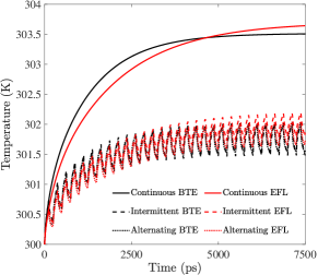
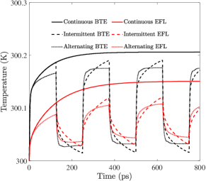
The evolution of transient peak temperature over time in bulk or SOI FinFET under three different heating strategies is shown in Fig. 7. From the profiles, it can be found that compared to the results in quasi-2D hotspot systems (Fig. 4), there are large deviations between the EFL and BTE solutions in 3D hotspot systems regardless of bulk or SOI FinFET. The temperature predicted by EFL rises more slowly than BTE at the initial stage, and it also takes longer to reach the periodic steady state. When the system reaches the periodic steady state, the transient temperature variance trend predicted by EFL is also inconsistent with the simulation result of BTE. For example, the ‘Intermittent’ heating strategy has a higher peak temperature rise than that of ‘Alternating’ heating strategy in the heating stage and has a lower peak temperature in the second half of the heating period in the BTE solutions. However, in the EFL prediction results, the maximum temperature of the ‘Alternating’ heating strategy is lower than that of the ‘Intermittent’ heating strategy in the second half of the heating period. Compared to ‘Intermittent’ heating, the temperature variance of ‘Alternating’ heating is smaller, which is similar to the results of quasi-2D hotspot systems (Fig. 4).
In order to further study the transient heat conduction in bulk or SOI FinFET under ‘Intermittent’ or ‘Alternating’ heating strategies, we also show the temperature contour map predicted by BTE at different moments when the system reaches the periodic steady state in Figs. 8, 9, 10 and 11. For example, represents that the current moment is a quarter of a heating period .


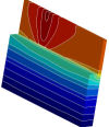
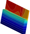
In bulk FinFET under ‘Intermittent’ heating, when the external heat source begins to heat the system, e.g., , the temperature near the heat source areas begins to rise continuously, and the high thermal energy in the fin region is rapidly transferred from hotspot area to other geometric regions by phonon ballistic transport. It can be seen from Fig. 8(a) that at the contact interface between the silicon fin and the silicon dioxide insulation layer, the temperature in the silicon region is higher than that of the silicon dioxide region at the same height. With the increase of time, the peak temperature of the system increases gradually until it reached a maximum at . But we can found that the temperature in the silicon region is lower than that of the silicon dioxide region at the same height when or . This is because the mean free path or thermal diffusivity rate of silicon is much higher than that of silicon dioxide, which leads to a higher heat dissipation efficiency. The thermal energy in silicon dioxide is mainly transferred from silicon to silicon dioxide through the interface, and then transferred to the bottom heat sink. However, as shown in Fig. 6(c), the heat dissipation efficiency of channel is much higher than that of . Although the thermal energy is transferred from silicon to silicon dioxide through the interface at the beginning , the energy in silicon dioxide is not efficiently transferred to the bottom heat sink due to its small mean free path, small thermal diffusivity and large interfacial thermal resistance. It is similar to a thermal reservoir. Over time, the silicon dioxide region actually got hotter, even higher than that of silicon at the same height. When the heat source is removed , the peak temperature decreases significantly due to the large mean free path of silicon.
In SOI FinFET under ‘Intermittent’ heating, it is well known that the silicon dioxide insulation layer is mainly introduced to improve electrical performance in the actual chip design [1, 5], but inevitably, it increases the temperature of silicon fin area due to low thermal conductivity. From Fig. 9, it can be observed that the temperature of the silicon fin region changes dramatically with time in a heating period, which actually generates a large thermal shock to the materials. Oppositely, the temperature contour profiles in the silicon dioxide insulation layer and silicon substrate region are basically flat, showing a linear distribution. In other words, the silicon dioxide insulation layer reduces the thermal shock on the bottom substrate material although it raised the overall temperature in the fin area.
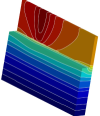
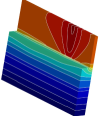
For ‘Alternating’ heating, two external heat source heat the system in turn so that the thermal conduction characteristics in the direction are no longer symmetrical. Temperature contour in bulk or SOI FinFET at different moments under ‘Alternating’ heating when the system reaches the periodic steady state is plotted in Figs. 10 and 11. When , one heat source starts to provide thermal energy so that the hotspot temperature increases, while the other is removed so that the hotspot temperature decreases gradually. Therefore, compared to the ‘Intermittent’ heating in Figs. 8 and 9, we can see that there is always a high temperature hotspot in the silicon fin region. This actually reflects that the overall temperature in the silicon fin region under ‘Alternating’ heating fluctuates less over time than that of under ‘Alternating’ heating, which is also verified in Fig. 7. Less temperature fluctuations represents smaller thermal shock on materials, which could delay the material life to some extent.
4 CONCLUSION AND OUTLOOK
Steady/unsteady heat dissipation in nanoscale bulk or SOI transistors under different heating strategies is investigated by the phonon BTE. Results show that it is not easy to accurately capture the heat conduction in transistors by the EFL although the effect of boundary scattering on phonon transport is added into the effective thermal conductivity. There are still some deviations between the results of phonon BTE and EFL, especially near the hotspot areas where ballistic phonon transport dominates and the temperature diffusion is no longer valid. Although the silicon dioxide increases the peak temperature significantly, it makes the temperature profiles in the silicon dioxide insulation layer and silicon substrate region flat, which reduces the dramatic temperature fluctuations. Different heating strategies have great influence on the peak temperature rise and transient thermal dissipation process. Compared to ‘Intermittent’ heating, the temperature variance of ‘Alternating’ heating is smaller, which indicates that this heating strategy also reduces the dramatic temperature fluctuations. The current research is helpful to understand the phonon heat conduction mechanisms in nanoscale transistors, and plays a theoretical guiding role in slowing down the temperature fluctuations and improving the life of the device.
It is noted that the heat generated in the solid area is mainly taken away through liquid cooling in the current advanced transistors or microelectronic devices. That is, the heat sink in the actual solid heat conduction regions is not an isothermal boundary, but microchannels for gas-liquid phase change heat transfer [53]. In the future, we will consider the coupling of solid phonon heat conduction with gas-liquid phase change heat transfer.
Conflict of interest
No conflict of interest declared.
Acknowledgments
Q. L. acknowledges the support of the National Natural Science Foundation of China (52376068). C. Z. acknowledges the members of online WeChat Group: Device Simulation Happy Exchange Group, for extensive discussions. The authors acknowledge Beijng PARATERA Tech CO.,Ltd. for providing HPC resources that have contributed to the research results reported within this paper.
Appendix A Solution of effective Fourier’s law
Combined the effective Fourier’s law (EFL) and first law of thermodynamics leading to
| (18) |
where effective thermal conductivity in the present simulation is a scalar rather than a tensor for a given spatial position . Finite volume method is invoked and above diffusion equation in integral form over a control volume from time to can be written as follows,
| (19) | |||
| (20) |
where trapezoidal quadrature is used for the time integration of the diffusion and heat source terms, , is the volume of the cell , is the sets of face neighbor cells of cell , is the interface between the cell and cell , is the area of the interface , is the effective thermal conductivity at the cell interface , and is the normal of the interface directing from the cell to the cell . Above discretizations theoretically have second-order spatial and temporal accuracy. The time step is set as ps and Cartesian grids with uniform cell size nm is used in the solutions of EFL. Conjugate gradient method is used to solve this temperature diffusion equation (20).
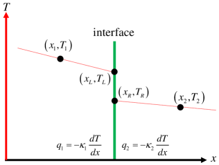
To solve Eq. (20), one of the key input parameter is the effective thermal conductivity at the interface between medium and . Let’s take the quasi-1D heat conduction as an example and briefly introduce how to deal with interface thermal resistance efficiently for macroscopic diffusion equation. Considering two discretized uniform cells adjacent to the interface between medium and with cell size , as shown in Fig. 1(c), there are different temperature distributions near the interface. The positions and temperatures of cell center are and , respectively. The positions and temperatures of the left and right limits of the interface are and , respectively, where . The heat flux at the left or right limit of the interface can be calculated based on the EFL,
| (21) | ||||
| (22) |
The heat flux across the interface can be calculated according to the definition of interface thermal resistance,
| (23) |
where [24]. Note that the heat flux at the left or right limit of the interface and the heat flux across the interface should be equal, i.e.,
| (24) |
Combined above four equations, we can obtain an approximated thermal conductivity at the interface,
| (25) | ||||
| (26) |
The effective thermal conductivity in the macroscopic diffusion equation (18) is
| (27) | ||||
| (28) |
where the boundary scattering rate is , is smallest characteristic length which depends on the spatial position . Specific values of in different spatial regions in this paper are list below. In quasi-2D hotspot system shown in Sec. 3.1 or Fig. 2(a), we set nm for pure silicon structure. For Si/SiO2/Si structure, the whole computational domain are decomposed by three parts. We set nm and nm in the top and bottom silicon areas, respectively. In bulk or SOI FinFET shown in Sec. 3.2 or Fig. 5(a), we set nm in the fin area and nm in the bottom silicon substrate areas. In the silicon dioxide, the bulk thermal conductivity W mK-1 is always used.
Appendix B Numerical discretizations and independence test
To solve the transient phonon BTE, the temporal space, solid angle space and spatial space are both discretized into a lot of small pieces. Time step is ps and Cartesian grids with uniform cell size nm is used. Solid angle is discretized into pieces, where is discretized by -point Gauss-Legendre quadrature and (due to symmetry) is discretized by the Gauss-Legendre quadrature with points. All numerical results are obtained by a three-dimensional C/C++ program. MPI parallelization computation with CPU cores based on the decomposition of solid angle space is implemented and the discrete solid angles corresponding to the specular reflection are ensured in the same CPU core.
Take the heat conduction in quasi-2D bulk structure (Fig. 2a) or 3D bulk FinFET (Fig. 5) as an example, we conduct an independent verification of the number of discrete solid angles. Steady temperature contour or heat flux contour under ‘Continuous’ heating source with different number of discrete solid angle is shown in Fig. 12. Numerical results show that discrete solid angles are not enough to accurately capture the non-diffusive heat conduction, and there is serious numerical jitter. Temperature fields predicted by BTE with or discretized solid angles are almost the same in quasi-2D simulations. Considering the huge computational amount of 3D simulation, we only use discrete points in order to take into account both accuracy and computational efficiency.
References
- IEEE [2023] IEEE, International Roadmap for Devices and Systems (IRDS™), IEEE, 2023. URL: https://irds.ieee.org/editions/2023.
- Stettler et al. [2021] M. A. Stettler, S. M. Cea, S. Hasan, L. Jiang, P. H. Keys, C. D. Landon, P. Marepalli, D. Pantuso, C. E. Weber, Industrial TCAD: Modeling atoms to chips, IEEE Transactions on Electron Devices 68 (2021) 5350–5357. doi:10.1109/TED.2021.3076976.
- Moore and Shi [2014] A. L. Moore, L. Shi, Emerging challenges and materials for thermal management of electronics, Mater. Today 17 (2014) 163–174. URL: https://www.sciencedirect.com/science/article/pii/S1369702114001138. doi:10.1016/j.mattod.2014.04.003.
- Pop [2010] E. Pop, Energy dissipation and transport in nanoscale devices, Nano Res. 3 (2010) 147–169. URL: https://doi.org/10.1007/s12274-010-1019-z. doi:10.1007/s12274-010-1019-z.
- Chhabria and Sapatnekar [2019] V. A. Chhabria, S. S. Sapatnekar, Impact of self-heating on performance and reliability in finfet and gaafet designs, in: 20th International Symposium on Quality Electronic Design (ISQED), 2019, pp. 235–240. doi:10.1109/ISQED.2019.8697786.
- Klemme et al. [2023] F. Klemme, S. Salamin, H. Amrouch, Upheaving self-heating effects from transistor to circuit level using conventional EDA tool flows, in: 2023 Design, Automation & Test in Europe Conference & Exhibition (DATE), 2023, pp. 1–6. doi:10.23919/DATE56975.2023.10137162.
- Hua et al. [2023] Y.-C. Hua, Y. Shen, Z.-L. Tang, D.-S. Tang, X. Ran, B.-Y. Cao, Chapter eight - near-junction thermal managements of electronics, Advances in Heat Transfer 56 (2023) 355–434. URL: https://www.sciencedirect.com/science/article/pii/S0065271723000096. doi:https://doi.org/10.1016/bs.aiht.2023.05.004.
- Zhang et al. [2021] C. Zhang, S. Chen, Z. Guo, L. Wu, A fast synthetic iterative scheme for the stationary phonon Boltzmann transport equation, Int. J. Heat Mass Transfer 174 (2021) 121308. URL: https://www.sciencedirect.com/science/article/pii/S0017931021004117. doi:10.1016/j.ijheatmasstransfer.2021.121308.
- Zhang et al. [2023] C. Zhang, S. Huberman, X. Song, J. Zhao, S. Chen, L. Wu, Acceleration strategy of source iteration method for the stationary phonon boltzmann transport equation, Int. J. Heat Mass Transfer 217 (2023) 124715. URL: https://www.sciencedirect.com/science/article/pii/S0017931023008608. doi:https://doi.org/10.1016/j.ijheatmasstransfer.2023.124715.
- Mazumder [2022] S. Mazumder, Boltzmann transport equation based modeling of phonon heat conduction: Progress and challenges, Annual Review of Heat Transfer 24 (2022) 71–130. URL: https://www.dl.begellhouse.com/references/5756967540dd1b03,3ae07302147f45b7,09643dee3a7e400e.html. doi:10.1615/AnnualRevHeatTransfer.2022041316.
- Barry et al. [2022] M. C. Barry, N. Kumar, S. Kumar, Boltzmann transport equation for thermal transport in electronic materials and devices, Annual Review of Heat Transfer 24 (2022) 131–172. URL: https://dl.begellhouse.com/references/5756967540dd1b03,3ae07302147f45b7,43e971b72ed09c31.html. doi:10.1615/AnnualRevHeatTransfer.v24.50.
- Liu et al. [2022] X. Liu, M. Fan, Y. Hu, H. Li, F. Liu, J. Kang, Simulation methods of multi-physics effects in nano-scale cmos, in: 2022 International Electron Devices Meeting (IEDM), 2022, pp. 15.4.1–15.4.4. doi:10.1109/IEDM45625.2022.10019403.
- Gu et al. [2018] X. Gu, Y. Wei, X. Yin, B. Li, R. Yang, Colloquium: phononic thermal properties of two-dimensional materials, Rev. Mod. Phys. 90 (2018) 041002. URL: https://link.aps.org/doi/10.1103/RevModPhys.90.041002. doi:10.1103/RevModPhys.90.041002.
- Honarvar et al. [2021] H. Honarvar, J. L. Knobloch, T. D. Frazer, B. Abad, B. McBennett, M. I. Hussein, H. C. Kapteyn, M. M. Murnane, J. N. Hernandez-Charpak, Directional thermal channeling: A phenomenon triggered by tight packing of heat sources, Proceedings of the National Academy of Sciences 118 (2021) e2109056118. URL: https://www.pnas.org/doi/abs/10.1073/pnas.2109056118. doi:10.1073/pnas.2109056118.
- Chen et al. [2018] X. Chen, C. Hua, H. Zhang, N. K. Ravichandran, A. J. Minnich, Quasiballistic thermal transport from nanoscale heaters and the role of the spatial frequency, Phys. Rev. Applied 10 (2018) 054068. URL: https://link.aps.org/doi/10.1103/PhysRevApplied.10.054068. doi:10.1103/PhysRevApplied.10.054068.
- Zhang et al. [2020] Z. Zhang, Y. Ouyang, Y. Cheng, J. Chen, N. Li, G. Zhang, Size-dependent phononic thermal transport in low-dimensional nanomaterials, Phys. Rep. 860 (2020) 1–26. URL: https://www.sciencedirect.com/science/article/pii/S0370157320300922. doi:10.1016/j.physrep.2020.03.001.
- Hao et al. [2018] Q. Hao, H. Zhao, Y. Xiao, Q. Wang, X. Wang, Hybrid electrothermal simulation of a 3-d fin-shaped field-effect transistor based on gan nanowires, IEEE Transactions on Electron Devices 65 (2018) 921–927. doi:10.1109/TED.2018.2791959.
- Landon et al. [2023] C. Landon, L. Jiang, D. Pantuso, I. Meric, K. Komeyli, J. Hicks, D. Schroeder, Localized thermal effects in gate-all-around devices, in: 2023 IEEE International Reliability Physics Symposium (IRPS), 2023, pp. 1–5. doi:10.1109/IRPS48203.2023.10117903.
- Jou et al. [2010] D. Jou, G. Lebon, J. Casas-Vázquez, Extended Irreversible Thermodynamics, 4 ed., Springer Netherlands, 2010. URL: https://www.springer.com/gp/book/9789048130733. doi:10.1007/978-90-481-3074-0.
- Sendra et al. [2021] L. Sendra, A. Beardo, P. Torres, J. Bafaluy, F. X. Alvarez, J. Camacho, Derivation of a hydrodynamic heat equation from the phonon boltzmann equation for general semiconductors, Phys. Rev. B 103 (2021) L140301. URL: https://link.aps.org/doi/10.1103/PhysRevB.103.L140301. doi:10.1103/PhysRevB.103.L140301.
- Joseph and Preziosi [1989] D. D. Joseph, L. Preziosi, Heat waves, Rev. Mod. Phys. 61 (1989) 41–73. URL: https://link.aps.org/doi/10.1103/RevModPhys.61.41. doi:10.1103/RevModPhys.61.41.
- Cattaneo [1948] C. Cattaneo, Sulla conduzione del calore, Atti Sem. Mat. Fis. Univ. Modena 3 (1948) 83–101.
- Chen et al. [2024] L. Chen, C. Zhang, J. Zhao, Modeling heat conduction with dual-dissipative variables: A mechanism-data fusion method, Phys. Rev. E 110 (2024) 025303. URL: https://link.aps.org/doi/10.1103/PhysRevE.110.025303. doi:10.1103/PhysRevE.110.025303.
- Zeng and Chen [2014] L. Zeng, G. Chen, Disparate quasiballistic heat conduction regimes from periodic heat sources on a substrate, J. Appl. Phys. 116 (2014) 064307. URL: https://aip.scitation.org/doi/10.1063/1.4893299. doi:10.1063/1.4893299.
- Zhang and Wu [2022] C. Zhang, L. Wu, Nonmonotonic heat dissipation phenomenon in close-packed hotspot systems, Phys. Rev. E 106 (2022) 014111. URL: https://link.aps.org/doi/10.1103/PhysRevE.106.014111. doi:10.1103/PhysRevE.106.014111.
- Hoogeboom-Pot et al. [2015] K. M. Hoogeboom-Pot, J. N. Hernandez-Charpak, X. Gu, T. D. Frazer, E. H. Anderson, W. Chao, R. W. Falcone, R. Yang, M. M. Murnane, H. C. Kapteyn, D. Nardi, A new regime of nanoscale thermal transport: Collective diffusion increases dissipation efficiency, Proc. Natl Acad. Sci. 112 (2015) 4846–4851. URL: https://www.pnas.org/content/112/16/4846. doi:10.1073/pnas.1503449112.
- Yang and Dames [2015] F. Yang, C. Dames, Heating-frequency-dependent thermal conductivity: An analytical solution from diffusive to ballistic regime and its relevance to phonon scattering measurements, Phys. Rev. B 91 (2015) 165311. URL: https://link.aps.org/doi/10.1103/PhysRevB.91.165311. doi:10.1103/PhysRevB.91.165311.
- Regner et al. [2013] K. T. Regner, D. P. Sellan, Z. Su, C. H. Amon, A. J. H. McGaughey, J. A. Malen, Broadband phonon mean free path contributions to thermal conductivity measured using frequency domain thermoreflectance, Nat. Commun. 4 (2013) 1–7. URL: https://www.nature.com/articles/ncomms2630. doi:10.1038/ncomms2630.
- Tang and Cao [2023] D.-S. Tang, B.-Y. Cao, Phonon thermal transport and its tunability in GaN for near-junction thermal management of electronics: A review, Int. J. Heat Mass Transfer 200 (2023) 123497. URL: https://www.sciencedirect.com/science/article/pii/S0017931022009668. doi:https://doi.org/10.1016/j.ijheatmasstransfer.2022.123497.
- Murthy et al. [2005] J. Y. Murthy, S. V. J. Narumanchi, J. A. Pascual-Gutierrez, T. Wang, C. Ni, S. R. Mathur, Review of multiscale simulation in submicron heat transfer, Int. J. Multiscale Computat. Eng. 3 (2005) 5–32. URL: http://dl.begellhouse.com/journals/61fd1b191cf7e96f,69f10ca36a816eb7,25fd09426d0aaf45.html. doi:10.1615/IntJMultCompEng.v3.i1.20.
- Pham et al. [2018] A.-T. Pham, S. Jin, Y. Lu, H.-H. Park, W. Choi, M. A. Pourghaderi, J. Kim, U. Kwon, D. Kim, Simulations of self-heating effects in sige pfinfets based on self-consistent solution of carrier/phonon bte coupled system, in: 2018 International Conference on Simulation of Semiconductor Processes and Devices (SISPAD), 2018, pp. 145–148. doi:10.1109/SISPAD.2018.8551670.
- Lofrano et al. [2023] M. Lofrano, H. Oprins, X. Chang, B. Vermeersch, O. V. Pedreira, A. Lesniewska, V. Cherman, I. Ciofi, K. Croes, S. Park, Z. Tokei, Towards accurate temperature prediction in BEOL for reliability assessment (invited), in: 2023 IEEE International Reliability Physics Symposium (IRPS), 2023, pp. 1–7. doi:10.1109/IRPS48203.2023.10117701.
- Chang et al. [2023] X. Chang, H. Oprins, M. Lofrano, V. Cherman, B. Vermeersch, J. D. Fortuny, S. Park, Z. Tokei, I. De Wolf, Calibrated fast thermal calculation and experimental characterization of advanced BEOL stacks, in: 2023 IEEE International Interconnect Technology Conference (IITC) and IEEE Materials for Advanced Metallization Conference (MAM)(IITC/MAM), 2023, pp. 1–3. doi:10.1109/IITC/MAM57687.2023.10154768.
- Xu et al. [2023] J. Xu, Y. Hu, H. Bao, Quantitative analysis of nonequilibrium phonon transport near a nanoscale hotspot, Phys. Rev. Appl. 19 (2023) 014007. URL: https://link.aps.org/doi/10.1103/PhysRevApplied.19.014007. doi:10.1103/PhysRevApplied.19.014007.
- Shen et al. [2023] Y. Shen, H.-A. Yang, B.-Y. Cao, Near-junction phonon thermal spreading in GaN HEMTs: A comparative study of simulation techniques by full-band phonon monte carlo method, Int. J. Heat Mass Transfer 211 (2023) 124284. URL: https://www.sciencedirect.com/science/article/pii/S0017931023004362. doi:https://doi.org/10.1016/j.ijheatmasstransfer.2023.124284.
- Sheng et al. [2024] Y. Sheng, S. Wang, Y. Hu, J. Xu, Z. Ji, H. Bao, Integrating first-principles-based Non-Fourier thermal analysis into nanoscale device simulation, IEEE Transactions on Electron Devices 71 (2024) 1769–1775. doi:10.1109/TED.2024.3357440.
- Yang et al. [2005] R. Yang, G. Chen, M. Laroche, Y. Taur, Simulation of nanoscale multidimensional transient heat conduction problems using ballistic-diffusive equations and phonon Boltzmann equation, J. Heat Transfer 127 (2005) 298–306. URL: http://dx.doi.org/10.1115/1.1857941. doi:10.1115/1.1857941.
- Adisusilo et al. [2014] I. N. Adisusilo, K. Kukita, Y. Kamakura, Analysis of heat conduction property in FinFETs using phonon Monte Carlo simulation, in: 2014 International Conference on Simulation of Semiconductor Processes and Devices (SISPAD), 2014, pp. 17–20. doi:10.1109/SISPAD.2014.6931552.
- Mukhopadhyay et al. [2018] S. Mukhopadhyay, A. Kundu, Y. Lee, H. D. Hsieh, D. Huang, J. Horng, T. Chen, J. Lee, Y. Tsai, C. Lin, R. Lu, J. He, An unique methodology to estimate the thermal time constant and dynamic self heating impact for accurate reliability evaluation in advanced FinFET technologies, in: 2018 IEEE International Electron Devices Meeting (IEDM), 2018, pp. 17.4.1–17.4.4. doi:10.1109/IEDM.2018.8614479.
- Warzoha et al. [2021] R. J. Warzoha, A. A. Wilson, B. F. Donovan, N. Donmezer, A. Giri, P. E. Hopkins, S. Choi, D. Pahinkar, J. Shi, S. Graham, Z. Tian, L. Ruppalt, Applications and impacts of nanoscale thermal transport in electronics packaging, J Electron. Packaging 143 (2021) 020804. URL: https://doi.org/10.1115/1.4049293. doi:10.1115/1.4049293.
- Guo and Xu [2016] Z. Guo, K. Xu, Discrete unified gas kinetic scheme for multiscale heat transfer based on the phonon Boltzmann transport equation, Int. J. Heat Mass Transfer 102 (2016) 944 – 958. URL: http://www.sciencedirect.com/science/article/pii/S0017931016306731. doi:10.1016/j.ijheatmasstransfer.2016.06.088.
- Pathak et al. [2021] A. Pathak, A. Pawnday, A. P. Roy, A. J. Aref, G. F. Dargush, D. Bansal, MCBTE: A variance-reduced monte carlo solution of the linearized boltzmann transport equation for phonons, Comput. Phys. Commun. 265 (2021) 108003. URL: https://www.sciencedirect.com/science/article/pii/S0010465521001156. doi:https://doi.org/10.1016/j.cpc.2021.108003.
- Pop et al. [2006] E. Pop, S. Sinha, K. Goodson, Heat generation and transport in nanometer-scale transistors, Proceedings of the IEEE 94 (2006) 1587–1601. doi:10.1109/JPROC.2006.879794.
- Medlar and Hensel [2022] M. P. Medlar, E. C. Hensel, Transient Three-Dimensional Thermal Simulation of a Fin Field-Effect Transistor With Electron–Phonon Heat Generation, Three Phonon Scattering, and Drift With Periodic Switching, ASME Journal of Heat and Mass Transfer 145 (2022) 022501. URL: https://doi.org/10.1115/1.4056002. doi:10.1115/1.4056002.
- Pop et al. [2004] E. Pop, R. W. Dutton, K. E. Goodson, Analytic band monte carlo model for electron transport in si including acoustic and optical phonon dispersion, J. Appl. Phys. 96 (2004) 4998–5005. URL: http://aip.scitation.org/doi/10.1063/1.1788838. doi:10.1063/1.1788838.
- Minnich [2012] A. J. Minnich, Determining phonon mean free paths from observations of quasiballistic thermal transport, Phys. Rev. Lett. 109 (2012) 205901. URL: https://link.aps.org/doi/10.1103/PhysRevLett.109.205901. doi:10.1103/PhysRevLett.109.205901.
- Goodson and Flik [1992] K. Goodson, M. Flik, Effect of microscale thermal conduction on the packing limit of silicon-on-insulator electronic devices, IEEE Transactions on Components, Hybrids, and Manufacturing Technology 15 (1992) 715–722. doi:10.1109/33.180035.
- Nasri et al. [2015] F. Nasri, M. Ben Aissa, H. Belmabrouk, Microscale thermal conduction based on cattaneo-vernotte model in silicon on insulator and double gate mosfets, Applied Thermal Engineering 76 (2015) 206–211. URL: https://www.sciencedirect.com/science/article/pii/S1359431114010564. doi:https://doi.org/10.1016/j.applthermaleng.2014.11.038.
- Chen et al. [2022] J. Chen, X. Xu, J. Zhou, B. Li, Interfacial thermal resistance: Past, present, and future, Rev. Mod. Phys. 94 (2022) 025002. URL: https://link.aps.org/doi/10.1103/RevModPhys.94.025002. doi:10.1103/RevModPhys.94.025002.
- Tian et al. [2024] S. Tian, T. Wu, S. Hu, D. Ma, L. Zhang, Boosting phonon transport across AlN/SiC interface by fast annealing amorphous layers, Applied Physics Letters 124 (2024) 042202. URL: https://doi.org/10.1063/5.0187793. doi:10.1063/5.0187793.
- Hao et al. [2017] Q. Hao, H. Zhao, Y. Xiao, A hybrid simulation technique for electrothermal studies of two-dimensional GaN-on-SiC high electron mobility transistors, J. Appl. Phys. 121 (2017) 204501. URL: https://doi.org/10.1063/1.4983761. doi:10.1063/1.4983761.
- Guo and Xu [2021] Z. Guo, K. Xu, Progress of discrete unified gas-kinetic scheme for multiscale flows, Adva. Aerodyn. 3 (2021) 6. URL: https://doi.org/10.1186/s42774-020-00058-3. doi:10.1186/s42774-020-00058-3.
- Van Erp et al. [2020] R. Van Erp, R. Soleimanzadeh, L. Nela, G. Kampitsis, E. Matioli, Co-designing electronics with microfluidics for more sustainable cooling, Nature 585 (2020) 211–216. URL: https://www.nature.com/articles/s41586-020-2666-1. doi:https://doi.org/10.1038/s41586-020-2666-1.