Native defects and -type dopability in transparent -TeO2: A first-principles study
Abstract
Although -\ceTeO2 is a promising -type transparent conducting oxide (TCO) due to the large optical gap ( 3.7 eV) and a light effective hole mass, its hole dopability still remains unexplored. In this work, electronic structure of -\ceTeO2 and its point defects are investigated using the HSEsol functional with the band-gap-tuned mixing parameter. Our calculations reveal that -\ceTeO2 exhibits a significant difference between the fundamental and optical band gaps because lower energy optical transitions are dipole forbidden. Additionally, it has a low hole effective mass, especially in-plane. The point defect calculations show that -\ceTeO2 is intrinsically an insulator. From systematic calculations of the trivalent dopants as well as hydrogen, Bi doping is suggested as the best candidate as an acceptor dopant. This work paves the way for the material design of the -type -\ceTeO2.
I Introduction
The – junction of transparent conducting oxides (TCOs) would be crucial for wide range of applications such as displays [1], bipolar transistors [2], photovoltaics [3], and inverter circuits [4]. Despite the availability of -type TCOs, such as Sn-doped In2O3 [5] and Al-doped ZnO [6], -type counterparts remain scarce due to the difficulty of hole doping and/or low hole mobility [7, 8].
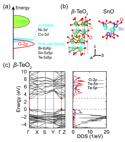
The main obstacle to -type doping in oxides originates from their electronic structures, where the valence band maxima (VBMs) consisting of O- states are too deep to introduce hole carriers. Therefore, the strategy for designing -type TCOs is to place the orbitals with higher energy levels above the O- bands [9], as illustrated in Fig. 1(a). Such strategy has been demonstrated with Ni- orbitals in NiO [10], Cu- orbitals in CuAlO2 [9, 11] and CuGaO2 [11, 12], Sn- and orbitals in SnO [13] and K2SnO2 [14], and Bi- and orbitals in BaBiO3 [15]. When additional orbitals are close to the O- orbitals in energy, they typically form covalent bonds with the O- bands. This results in another benefit: more dispersive valence bands with reduced hole effective masses.
Regarding SnO, although it shows the -type conductivity with a small hole effective mass [16], the optical band gap is 2.70 eV, which is slightly below the threshold to achieve transparency in the visible range. This motivates us to explore -type TCO candidates with similar lone pair characteristics as Sn2+ but with a higher optical gap.
TeO2 has been suggested as a possible candidate in the same manner as SnO because Te4+ has the same electronic configuration as Sn2+. We display electron localization functions [17] of -\ceTeO2 and \ceSnO in Fig. 1(b), both of which exhibit lone-pair orbitals composed of the mixture of and orbitals. The density of states (DOS) in -\ceTeO2 [Fig. 1(c)] shows that the VBM is lifted up by the presence of Te 5 and 5 lone pairs that hybridize with the O- bands. The -type behavior has been reported for a two-dimensional (2D) bilayer -\ceTeO2 with high hole mobility and high band gap around 3.7 eV [18]. Ab initio calculations and subsequent experiments have also confirmed its high hole mobility and small hole effective masses [19, 20, 21, 22, 23, 24].
According to the material properties, the three-dimensional (3D) -\ceTeO2 is expected to be a good candidate for a -type TCO due to its large optical band gap and small hole effective mass [19]. Moreover, in view of the defect perspectives, since Te and O have very different ionic radii (0.66 and 1.35 in the 4-coordination [25]), the formation of antisite-type defects that often cause the Fermi-level pinning within the band gap are expected to be prohibitive. However, the experimental report of the -type conduction is still limited to a 2D field-effect transistor (FET) -\ceTeO2 [18].
To achieve fundamental insight of -type behavior of 3D -\ceTeO2, we investigate the intrinsic defects and -type dopants using the HSEsol hybrid functional [26, 27, 28, 29]. We first discuss the electronic structures of the TeO2 polymorphs. We have found that only -\ceTeO2 exhibits a significant difference between the fundamental gap and the optical band gap because the lower energy optical transitions are dipole forbidden. For the calculations of the intrinsic defects in -\ceTeO2, vacancies, antisites, and interstitials were considered and equilibrium Fermi levels and carrier concentrations were estimated. Trivalent acceptor dopants as well as hydrogen impurities were also calculated. Consequently, Bi was suggested as the best -type dopant exhibiting the acceptor transition around 0.47 eV. Furthermore, we propose to dope acceptors in high concentrations to reduce the acceptor levels.
Initially, the computational details are explained in Sec. II. The electronic structures and optical properties of the \ceTeO2 polymorphs are then discussed in Sec. III.1. In Secs. III.2 and III.3, the formation energies of intrinsic defects and impurities in -\ceTeO2 are discussed, respectively. Finally, the conclusion is summarized in Sec. IV.
II Computational details
First-principles calculations were performed using the projector augmented-wave (PAW) method [30, 31], as implemented in VASP [32]. Te- and , and O- were then described as valence electrons. Information on the PAW datasets and the valence electrons of the other elements are provided in the Supplementary Material. The HSEsol functional, i.e., the combination of the Heyd-Scuseria-Ernzerhof (HSE) hybrid functional with the PBEsol functional was employed [26]. The screening distance is then fixed at 0.2 , and the Fock exchange mixing parameter is tuned to to reproduce the experimental optical band gap of -\ceTeO2 [see Sec. III(a)]. The plane-wave cutoff energy was set to 520 eV for structure optimization to reduce the Pulay stress and to 400 eV for the other calculations.
For the structure optimization and band structure calculations, 443, 332 and 442 -point grids were used for the , , and phases, respectively. For metals and insulators that were calculated for constructing the chemical potential diagrams (CPDs), the -point densities were set to 2.5 and 5.0, respectively. The force and stress convergence criteria were set to 5 meV/Å and 0.08 GPa, respectively. The effective mass tensors, DOS, and dielectric functions were calculated with tripled -points along all three directions to enhance the accuracy. The static dielectric tensors () were calculated from the sum of the ion-clamped () and ionic dielectric contributions () based on the density functional perturbation theory [33, 34, 35]. The were obtained from the HSEsol calculations, whereas the were acquired from the PBEsol calculations to reduce the computational costs. For the , the local field effects are included.
The band-averaged effective mass tensors were calculated using BoltzTraP2 [36], with the carrier concentration and temperature set to and 300, respectively. For the calculations of the optical absorption spectra, the real parts of the dielectric functions were derived from the imaginary parts via the Kramers-Kronig transformation with a complex shift of 0.01 eV [36]. The optical band gaps were determined from the Tauc plots to maintain consistency with experimental optical measurements [19].
The band paths were automatically set using SeeK-path [37]. The irreducible representations of the electronic bands at the point were determined using the IrRep code [38, 39].
For the defect calculations, we adopted a 221 supercell of the conventional unit cell of -\ceTeO2 with 96 atoms and -\ceTeO2 with 48 atoms. A 221 Monkhorst-Pack -point mesh [40] was used for –\ceTeO2, and a 222 mesh was used for -\ceTeO2. The internal atomic positions were relaxed until the residual forces were reduced to less than 30 with fixed theoretical lattice constants. In all the defect calculations, spin polarization was allowed.
We constructed the CPDs using the total energies, ignoring vibrational and entropy contributions. In this study, we retrieved the candidate competing phases that are either stable or slightly unstable by 0.01 meV/atom from the Materials Project [41]. For the standard state of O, we calculated an \ceO2 molecule in the spin triplet configuration. See also the Supplementary Material for the list of the competing phases considered in this study.
We used the VISE code (version 0.6.6) to generate all the VASP input settings, and PYDEFECT [42] to generate the defect models and to analyze the first-principles calculation results. The formula to calculate the formation energy of defect in charge () is described elsewhere [43]. We corrected the defect formation energies of charged defects using the extended FNV method as described in [44, 45, 46].
The effective value between , , is evaluated as [47]
| (1) |
The carrier concentrations as a function of the Fermi level were calculated from the DOS via the Fermi-Dirac distribution [46]. The defect concentrations were estimated from the Boltzmann distribution, considering the site degeneracies that depend on the defect site symmetries in the relaxed structures and the spin degeneracies [46].
III Results and discussion
III.1 Fundamental properties of TeO2 polymorphs
| Lattice constants | Dielectric constants | ||||||
| Phase | Direction | Exp. (Å) | Calc. (Å) | Diff() | Ion-clamped | Ionic | |
| 4.808 | 4.78 | 1.85 | 4.9 | 18.8 | |||
| 7.612 | 7.49 | 3.69 | 5.6 | 20.5 | |||
| 5.464 | 5.30 | 0.75 | 4.7 | 22.1 | |||
| 5.607 | 5.62 | 0.74 | 5.5 | 18.4 | |||
| 12.035 | 12.07 | 2.23 | 4.2 | 4.7 | |||
| 4.898 | 4.84 | 6.88 | 4.6 | 9.2 | |||
| 4.351 | 4.32 | 3.35 | 4.4 | 9.0 | |||
| 8.576 | 8.64 | 2.31 | 4.9 | 15.4 | |||
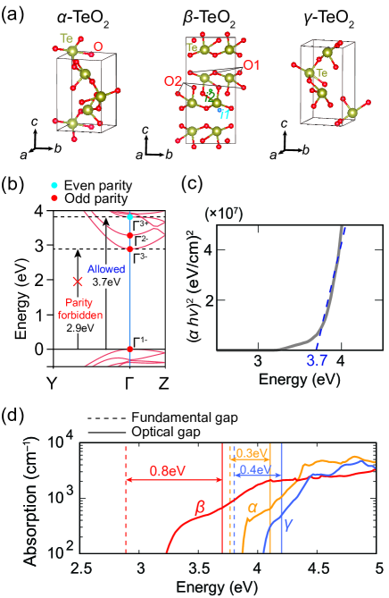
TeO2 has three polymorphs: -\ceTeO2 [48], -\ceTeO2 [49], and -\ceTeO2 [50]. As illustrated in Figs. 2(a), each Te atom is surrounded by four O atoms, forming a \ceTeO4 disphenoid network. Different from - and -\ceTeO2 phases, -\ceTeO2 has a 2D layered structure in the – plane with the \ceTeO4 network being disconnected along the -direction.
As demonstrated for -\ceTeO2 in Fig. 1(c), the valence bands in three \ceTeO2 phases are mainly formed from O- states hybridized with Te-5 and Te-5 states. The electronic structures of the - and -\ceTeO2 phases are also provided in the Supplementary Material. Consequently, the VBM of -\ceTeO2 is raised in energy from the top of the O- bands by about 1.5 eV, which can make -type doping easier, as discussed in Sec. I. On the other hand, the conduction band is primarily composed of the Te- orbitals.
Here, we determine the optical band gaps from the Tauc plots, to keep the consistency with experiment [19]. Figure 2(c) shows against ; its linear extrapolation is used to determine the direct-allowed dipole transition gap. As shown, the -intercept exactly matches the experimental value of 3.7 eV, indicating the adequacy of .
The calculated fundamental direct gap with is 2.9 eV, much smaller than the optical gap. This is primarily because the transitions from the VBM located at the point to the lowest and second-lowest unoccupied states at the point are dipole forbidden as shown in Fig. 2(b).
Such a smaller fundamental gap is advantageous for doping in general, as exemplified by In2O3 [51]. Using the same mixing parameter, we obtain fundamental gaps of 3.8 eV for both - and -TeO2, with optical gaps of 4.1 and 4.2 eV, respectively. Therefore, the smaller fundamental gap is unique to the phase [see also their optical absorption spectra in Fig. 2(d)] 111Ref. [21] has reported the optical absorption spectrum of -\ceTeO2, but their calculated absorbance differs from ours by about a factor of 100..
Table 1 summarizes the calculated lattice constants alongside the available experimental values [48, 49, 50]. The differences are less than in most cases: an exception is the lattice constant of -TeO2, which is underestimated by about 3%. Note that, however, we have confirmed that the calculated band gap at the experimental lattice constants is the same as that at the theoretical lattice constants.
Regarding the hole effective masses (), -TeO2 generally exhibits smaller compared to the other phases. Notably, in the – plane is only 0.74–0.75 , where is the free-electron rest mass. This is comparable to the calculated value of 0.84 and 1.06 along the X– and Y– directions by Shi et al. [19], and that for the bilayer of -\ceTeO2 (0.51 ) by Zavabeti et al. [18].
III.2 Native point defects
| (K) | (eV) | |||||||
| 623 | 1.21 | 2 | 5 | 5 | 2 | – | – | 4 |
| 300 | 0.53 | 2 | – | 5 | 1 | – | – | 3 |
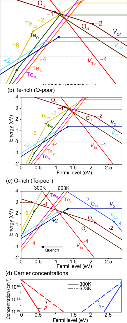
Since the phase has a lower fundamental gap while maintaining transparency and a lower hole effective mass, especially in the – plane, it should be the most suitable phase as a -type TCO. Hereinafter, we thus focus on investigating native defects and hole dopability in the phase. The unit cell of -\ceTeO2 consists of two TeO2 layers, and holds two distinct oxygen sites: one outside the layer (O1) and the other within the layer (O2) [see Fig. 2(a)]. In this study, we investigate Te and O vacancies (, ), and Te-on-O and O-on-Te antisites (Te, Te, and O). We also calculated interstitial sites, the initial positions of which are at the locations with the lowest () and second-lowest () charge density in the unit cell, as shown in Fig. 2(a). We calculated Te and O at these two sites ( and , ).
In -TeO2, based on the typical oxidation number of O, we would expect the oxidation states of Te and O to be and , respectively. We calculated the from to for and from to for since the closed-shell electronic structures of and are realized at and charge states, respectively. In contrast, we calculated the from to for Tei and from to for Oi in an opposite manner. For the substituted defects, we calculated a set of by regarding them as combinations of vacancies and interstitials. For example, Te is composed of Tei and . Thus, we considered from to for it. On the flip side, from to are considered for O. Based on their charge states, the candidate donor-type defects are , , and , whereas the candidate acceptor-type defects are , , and .
The CPD of the Te-O binary system is shown in Fig. 3(a). At the Te-rich (O-rich) condition, \ceTeO2 is equilibrated with Te (\ceTe2O5). Figures 3(b) and (c) show formation energies of the native defects at the Te-rich and O-rich conditions, which correspond to vertices A and B in Fig. 3(a), respectively.
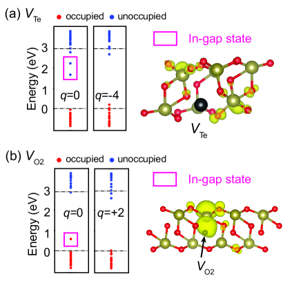
at makes very deep donor pinning level even at the Te-rich condition, which may lead to difficulties for synthesizing the -type -\ceTeO2. When we plot the eigenvalues of , any obvious in-gap states are not found, whereas there are two unoccupied states in the band gap at . Consequently, the stable charge state of transits from to , depending on the Fermi level (see also the Supplementary Material). The unoccupied in-gap states at are composed of the neighboring Te- and - orbitals hybridized with the O- orbitals, as shown in Fig. 4(a).
In contrast, creates a relatively shallower acceptor pinning level at around 0.1 eV at the O-rich condition. On the other hand, has a slightly higher energy, resulting in absence of the pinning level. The for and are and eV, respectively. Such negative behavior for oxygen vacancies has been commonly reported in representative oxides like ZnO [54] and MgO [55]. However, in contrast to the electride-like F-center states reported in ZnO and MgO, two (one) electrons at () are captured by the neighboring Te atom in -\ceTeO2 [see Fig. 4(b)].
Among the other native defects, only take relatively lower formation energies. Especially, pins the Fermi level at 0.34 eV even at the O-rich condition, setting a lower limit for the Fermi level, where cm-3 holes are introduced at 300 K as shown in Fig. 3(d). Such hole concentration is insufficient for semiconductor applications. The chemical potentials at the O-rich condition are determined from the total energies of \ceTe2O5 and \ceTeO2. However, the Te chemical potential might be further decreased to suppress Tei when the sample is synthesized, for instance, at high oxygen partial pressure, with suppressing the competing \ceTe2O5 and \ceTeO3.
Figure 3(c) and (d) and Table 2 present the Fermi level, as well as the defect and carrier concentrations, based on the charge neutrality condition [46] at the O-rich condition. The temperature is then set to 623 K, following the growth temperature in the experiment [19]. The equilibrium Fermi level is primarily determined by and . However, their formation energies are so high that their concentrations are extremely low. Consequently, the Fermi level is located in the middle of the band gap, resulting in an intrinsically insulating behavior.
We also calculated the Fermi level at 300 K assuming that the defect concentrations are quenched from 623 K, with taking different charge states in the ratio determined by the Boltzmann distribution [46]. After the quench, the Fermi level is largely shifted from 1.21 eV to 0.53 eV. Since the Fermi level does not cross the transition levels of the dominant defects, i.e., and , the hole carrier and dominant defect concentrations remain unchanged during the quench.
III.3 -type dopability of -TeO2
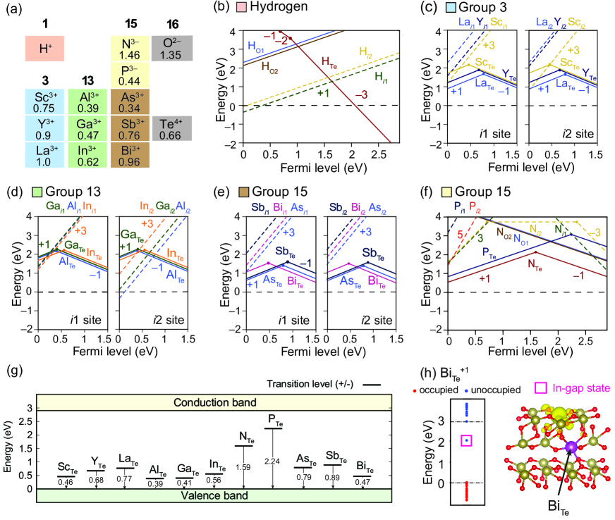
Since -\ceTeO2 is intrinsically insulating even at the O-rich condition, we consider 11 elements as acceptor dopants whose oxidation states and ionic radii are shown in Fig. 5(a). In addition, we considered the hydrogen impurity, as it is the most ubiquitous impurity in semiconductors and insulators [56]. Group 3 and 13 elements (Sc, Y, La, Al, Ga, and In) generally take oxidation states and are expected to introduce holes while substituting Te. The N and P in group 15 are considered to act as acceptors by placing at the O site with their oxidation states. As, Sb, and Bi are also expected to behave as acceptors at both Te and O sites due to their amphoteric behaviors by taking or oxidation states. The calculated formation energies of the dopants at the O-rich conditions are shown in Figs. 5(b)–(f). The calculated competing phases composed of the impurity elements at the O-rich condition are tabulated in the Supplementary Material.
As shown in Fig. 5(b), the hydrogen interstitial shows a Fermi level pinning at around 0.4 eV similar with Tei2 [see Fig. 3(c)], which is not beneficial to the -type doping. Thus, the hydrogen partial pressure should be minimized through, e.g., post-process annealing. In turn, H defects act as donors at any Fermi level within the band gap, but their energies are considerably high at the O-rich condition.
Calculation results of group 3 (Sc, Y, La), 13 (Al, Ga, In), and 15 (N, P, As, Sb, Bi) elements are shown in Figs. 5(c)–(f). When they are substituted to Te, they behave as acceptors, as expected from their oxidation states. Among As, Sb, and Bi, Bi shows a shallower acceptor level. N and P exhibit the lowest formation energies with amphoteric behaviors, similar to the other elements considered, but their transition levels are much higher (1.59 and 2.24 eV, respectively). It should be noted that they exhibit a negative behavior in common, where and charge states become more stable over the states for the whole range of the Fermi level. The widely range between and eV (see the Supplementary Material for their values).
The transitions are ranged in 0.39 – 0.77 eV above the VBM [see Fig. 5(g)], meaning the introduced holes are tightly bound compared to the shallow hydrogentic states, where the simple model estimates the acceptors level around 40 meV from the spherically averaged dielectric constant and effective mass shown in Table. 1 [57]. The electronic structure of Bi is shown in Fig. 5(h). When introducing a Bi at , two holes are captured by a lone pair state at the neighboring Te. We also calculated the two localized holes without Bi, namely we replace Bi with Te and change the number of electrons to retain the two holes. Consequently, we have found such localized holes are not stabilized energetically without help of attractive electrostatic interaction from a negatively charged Bi. In other words, the self-trapped holes are unstable in -\ceTeO2.
The formation energies of the interstitials are also shown in Figs. 5(b)–(f). Since interstitials exhibit positive charge states, they compensate hole carriers. The formation energy of the interstitial is generally lower as the ionic radius decreases. Thus, dopants with relatively large ionic radii could be more preferential for the acceptor doping. An exception is Bi, which shows a lower formation energy than Sb, though it has a larger ionic radius. Although the transition level of Bi is slightly higher than that of Al, the interstitial formation energies are high enough not to self-compensate. Therefore, Bi could be the best acceptor dopant.
The transition level of Bi is still located at 0.47 eV, close to the equilibrium Fermi level at the O-rich condition at 300K [see Fig. 3(c)], at which the hole concentration is estimated to be around [Fig. 3(d)]. Since successful fabrication of -type FET with -TeO2 has been reported [58], we also calculated Bi in -TeO2 with the same . The acceptor level of Bi is found at around 1.0 eV, which is about 0.5 eV deeper than the acceptor level in -\ceTeO2 (see the Supplementary Material). This implies that FET devices should be realized not only with the 2D phase [18] but also with the 3D phase in experiments.
In addition, is adjusted to match the optical band gap rather than the band edges in this study. This implies that there is a possibility that the actual VBM is higher in energy, leading to shallower acceptor levels than our calculations. Furthermore, when forming acceptor-type impurity levels near the VBM with considerable dopant concentration, it is possible to form an impurity band that can merge with the valence band and provide mobile hole carriers [59, 60]. Therefore, we suggest introducing Bi dopant at high concentrations under O-rich and H-poor conditions in experiments.
IV Conclusions
In this study, we have investigated the potential of -\ceTeO2 as a new transparent conducting oxide. Based on our calculations using a band-gap-tuned hybrid functional, it exhibits transparency but a smaller fundamental gap than the optical gap, which is advantageous for carrier doping. We have also found the in-plane hole effective mass is only 0.74–0.75 , indicating its good hole conductivity.
Our investigation into the native defects of -\ceTeO2 shows that it is intrinsically insulating regardless of the growth condition. Furthermore, we evaluated the formation energies and transition levels of 11 acceptor dopants and a hydrogen impurity. We found that although none of the acceptor dopants exhibit hydrogenic states, Sc, Al, Ga, and Bi show relatively shallower acceptor levels when substituted for the Te site. The absence of shallow hydrogenic states is attributed to the stabilization of the localized holes by the attractive electrostatic interaction from the acceptor dopants. Considering the formation energies of various types of defects, we suggest that -type doping may be achieved by doping Bi at a high concentration under O-rich and H-poor conditions.
Acknowledgement
This research has been financially supported by JSPS KAKENHI Grant Number 22H01755 and 23KF0030 and the E-IMR project at IMR, Tohoku University. Part of calculations were conducted using MASAMUNE-IMR (Project No. 202312-SCKXX-0408) and ISSP supercomputers.
References
- Afre et al. [2018] R. A. Afre, N. Sharma, M. Sharon, and M. Sharon, Rev. Adv. Mater. Sci. 53, 79 (2018).
- Arai et al. [2017] T. Arai, S. Iimura, J. Kim, Y. Toda, S. Ueda, and H. Hosono, J. Am. Chem. Soc. 139, 17175 (2017).
- Al-Ezzi and Ansari [2022] A. S. Al-Ezzi and M. N. M. Ansari, Appl. Syst. Innov. 5 (2022).
- Shijeesh et al. [2019] M. R. Shijeesh, P. A. Mohan, and M. K. Jayaraj, J. Electron. Mater. 49, 537 (2019).
- Kim and Lee [2020] D. Kim and S. Lee, Sci. Rep. 10, 4957 (2020).
- Majumder et al. [2003] S. Majumder, M. Jain, P. Dobal, and R. Katiyar, Mater. Sci. Eng. B. 103, 16 (2003).
- Kumagai [2023] Y. Kumagai, Phys. Rev. Appl. 19, 034063 (2023).
- Gake et al. [2019] T. Gake, Y. Kumagai, and F. Oba, Phys. Rev. Mater. 3, 044603 (2019).
- Kawazoe et al. [1997] H. Kawazoe, M. Yasukawa, H. Hyodo, M. Kurita, H. Yanagi, and H. Hosono, Nature 389, 939 (1997).
- Molaei et al. [2013] R. Molaei, R. Bayati, and J. Narayan, Cryst. Growth Des. 13, 5459 (2013).
- Gake et al. [2021] T. Gake, Y. Kumagai, A. Takahashi, and F. Oba, Phys. Rev. Mater. 5, 104602 (2021).
- Ueda et al. [2001] K. Ueda, T. Hase, H. Yanagi, H. Kawazoe, H. Hosono, H. Ohta, M. Orita, and M. Hirano, J. Appl. Phys. 89, 1790 (2001).
- Varley et al. [2013] J. B. Varley, A. Schleife, A. Janotti, and C. G. Van de Walle, Appl. Phys. Lett. 103, 082118 (2013).
- Hautier et al. [2013] G. Hautier, A. Miglio, G. Ceder, G.-M. Rignanese, and X. Gonze, Nat. Commun. 4, 2292 (2013).
- Schoop et al. [2013] L. M. Schoop, L. Müchler, C. Felser, and R. J. Cava, Inorg. Chem. 52, 5479 (2013).
- Allen et al. [2013] J. P. Allen, D. O. Scanlon, L. F. J. Piper, and G. W. Watson, J. Mater. Chem. C 1, 8194 (2013).
- Silvi and Savin [1994] B. Silvi and A. Savin, Nature 371, 683 (1994).
- Zavabeti et al. [2021] A. Zavabeti, P. Aukarasereenont, H. Tuohey, N. Syed, A. Jannat, A. Elbourne, K. A. Messalea, B. Y. Zhang, B. J. Murdoch, J. G. Partridge, M. Wurdack, D. L. Creedon, J. van Embden, K. Kalantar-Zadeh, S. P. Russo, C. F. McConville, and T. Daeneke, Nat. Electron. 4, 277 (2021).
- Shi et al. [2023] J. Shi, Z. Sheng, L. Zhu, X. Xu, Y. Gao, D. Tang, and K. H. L. Zhang, Appl. Phys. Lett. 122, 101901 (2023).
- Guo et al. [2022] S. Guo, H. Qu, W. Zhou, S. A. Yang, Y. S. Ang, J. Lu, H. Zeng, and S. Zhang, Phys. Rev. Appl. 17, 064010 (2022).
- Nguyen et al. [2024] H. H. Nguyen, R. T. Macaluso, and M. N. Huda, J. Phys. Chem. C. 128, 1728 (2024).
- Roginskii et al. [2017] E. M. Roginskii, V. G. Kuznetsov, M. B. Smirnov, O. Noguera, J.-R. Duclère, M. Colas, O. Masson, and P. Thomas, J. Phys. Chem. C. 121, 12365 (2017).
- Suehara et al. [2004] S. Suehara, P. Thomas, A. Mirgorodsky, T. Merle-Méjean, J. Champarnaud-Mesjard, T. Aizawa, S. Hishita, S. Todoroki, T. Konishi, and S. Inoue, J. Non-Cryst. Solids. 345-346, 730 (2004).
- Guo et al. [2018] S. Guo, Z. Zhu, X. Hu, W. Zhou, X. Song, S. Zhang, K. Zhang, and H. Zeng, Nanoscale 10, 8397 (2018).
- Shannon [1976] R. D. Shannon, Acta Crystallogr. Sect. A 32, 751 (1976).
- Schimka et al. [2011] L. Schimka, J. Harl, and G. Kresse, J. Chem. Phys. 134, 024116 (2011).
- Heyd et al. [2003] J. Heyd, G. E. Scuseria, and M. Ernzerhof, J. Chem. Phys. 118, 8207 (2003).
- Heyd et al. [2006] J. Heyd, G. E. Scuseria, and M. Ernzerhof, J. Chem. Phys. 124, 219906 (2006).
- Krukau et al. [2006] A. V. Krukau, O. A. Vydrov, A. F. Izmaylov, and G. E. Scuseria, J. Chem. Phys. 125, 224106 (2006).
- Blöchl [1994] P. E. Blöchl, Phys. Rev. B 50, 17953 (1994).
- Kresse and Joubert [1999] G. Kresse and D. Joubert, Phys. Rev. B 59, 1758 (1999).
- Kresse and Furthmüller [1996] G. Kresse and J. Furthmüller, Phys. Rev. B 54, 11169 (1996).
- Baroni and Resta [1986] S. Baroni and R. Resta, Phys. Rev. B 33, 7017 (1986).
- Gajdoš et al. [2006] M. Gajdoš, K. Hummer, G. Kresse, J. Furthmüller, and F. Bechstedt, Phys. Rev. B 73, 045112 (2006).
- Nunes and Gonze [2001] R. W. Nunes and X. Gonze, Phys. Rev. B 63, 155107 (2001).
- Madsen et al. [2018] G. K. Madsen, J. Carrete, and M. J. Verstraete, Comput. Phys. Commun. 231, 140 (2018).
- Hinuma et al. [2017] Y. Hinuma, G. Pizzi, Y. Kumagai, F. Oba, and I. Tanaka, Comput. Mater. Sci. 128, 140 (2017).
- Iraola et al. [2022] M. Iraola, J. L. Mañes, B. Bradlyn, M. K. Horton, T. Neupert, M. G. Vergniory, and S. S. Tsirkin, Comput. Phys. Commun. 272, 108226 (2022).
- Elcoro et al. [2017] L. Elcoro, B. Bradlyn, Z. Wang, M. G. Vergniory, J. Cano, C. Felser, B. A. Bernevig, D. Orobengoa, G. de la Flor, and M. I. Aroyo, J. Appl. Crystallogr. 50, 1457 (2017).
- Monkhorst and Pack [1976] H. J. Monkhorst and J. D. Pack, Phys. Rev. B 13, 5188 (1976).
- Jain et al. [2013] A. Jain, S. P. Ong, G. Hautier, W. Chen, W. D. Richards, S. Dacek, S. Cholia, D. Gunter, D. Skinner, G. Ceder, and K. A. Persson, APL Materials 1, 011002 (2013).
- Kumagai et al. [2021] Y. Kumagai, N. Tsunoda, A. Takahashi, and F. Oba, Phys. Rev. Mater. 5, 123803 (2021).
- Oba and Kumagai [2018] F. Oba and Y. Kumagai, Appl. Phys. Express. 11, 060101 (2018).
- Freysoldt et al. [2009] C. Freysoldt, J. Neugebauer, and C. G. Van de Walle, Phys. Rev. Lett. 102, 016402 (2009).
- Kumagai and Oba [2014] Y. Kumagai and F. Oba, Phys. Rev. B 89, 195205 (2014).
- Kumagai et al. [2014] Y. Kumagai, M. Choi, Y. Nose, and F. Oba, Phys. Rev. B 90, 125202 (2014).
- Kumagai et al. [2023] Y. Kumagai, S. R. Kavanagh, I. Suzuki, T. Omata, A. Walsh, D. O. Scanlon, and H. Morito, PRX Energy 2, 043002 (2023).
- Thomas [1988] P. A. Thomas, J. Phys. C: Solid State Phys. 21, 4611 (1988).
- BEYER [1967] H. BEYER, Zeitschrift für Kristallographie - Crystalline Materials 124, 228 (1967).
- Champarnaud-Mesjard et al. [2000] J. Champarnaud-Mesjard, S. Blanchandin, P. Thomas, A. Mirgorodsky, T. Merle-Méjean, and B. Frit, J. Phys. Chem. Solids. 61, 1499 (2000).
- Walsh et al. [2008] A. Walsh, J. L. F. Da Silva, S.-H. Wei, C. Körber, A. Klein, L. F. J. Piper, A. DeMasi, K. E. Smith, G. Panaccione, P. Torelli, D. J. Payne, A. Bourlange, and R. G. Egdell, Phys. Rev. Lett. 100, 167402 (2008).
- Note [1] Ref. [21] has reported the optical absorption spectrum of -\ceTeO2, but their calculated absorbance differs from ours by about a factor of 100.
- Momma and Izumi [2011] K. Momma and F. Izumi, J. Appl. Crystallogr. 44, 1272 (2011).
- Oba et al. [2008] F. Oba, A. Togo, I. Tanaka, J. Paier, and G. Kresse, Phys. Rev. B 77, 245202 (2008).
- Tanaka et al. [2002] I. Tanaka, F. Oba, K. Tatsumi, M. Kunisu, M. Nakano, and H. Adachi, Mater. Trans. 43, 1426 (2002).
- Van de Walle and Neugebauer [2003] C. G. Van de Walle and J. Neugebauer, Nature 423, 626 (2003).
- Yu and Cardona [2010] P. Yu and M. Cardona, Fundamentals of semiconductors:, Vol. Physics and materials properties (Springer Science & Business Media, 2010) p. 167.
- Devabharathi et al. [2024] N. Devabharathi, S. Yadav, I. Dönges, V. Trouillet, and J. J. Schneider, Adv. Mater. Interfaces. 11, 2301082 (2024).
- Samarth [2012] N. Samarth, Nat. Mater. 11, 360 (2012).
- Wang et al. [2019] D. Wang, D. Han, D. West, N.-K. Chen, S.-Y. Xie, W. Q. Tian, V. Meunier, S. Zhang, and X.-B. Li, npj Comput. Mater. 5, 8 (2019).