vario\fancyrefseclabelprefixSec. #1 \frefformatvariothmTheorem #1 \frefformatvariotblTbl. #1 \frefformatvariolemLemma #1 \frefformatvariocorCorollary #1 \frefformatvariodefDefinition #1 \frefformatvario\fancyreffiglabelprefixFig. #1 \frefformatvarioappAppendix #1 \frefformatvario\fancyrefeqlabelprefix(#1) \frefformatvariopropProposition #1 \frefformatvarioexmplExample #1 \frefformatvarioalgAlgorithm #1
A 46 Gbps 12 pJ/b Sparsity-Adaptive Beamspace Equalizer for mmWave Massive MIMO in 22FDX
Abstract
We present a GlobalFoundries 22FDX FD-SOI application-specific integrated circuit (ASIC) of a beamspace equalizer for millimeter-wave (mmWave) massive multiple-input multiple-output (MIMO) systems. The ASIC implements a recently-proposed power-saving technique called sparsity-adaptive equalization (SPADE). SPADE exploits the inherent sparsity of mmWave channels in the beamspace domain to reduce the dynamic power of matrix-vector products by skipping multiplications for which the magnitude of both operands are below pre-defined thresholds. Simulations with realistic mmWave channels show that SPADE incurs less than 0.7 dB SNR degradation at 1% target bit error rate compared to antenna-domain equalization. ASIC measurement results demonstrate an equalization throughput of 46 Gbps and show that SPADE offers up to 38% power savings compared to antenna-domain equalization. A comparison with state-of-the-art massive MIMO equalizer designs reveals that our ASIC achieves superior normalized energy efficiency.
I Introduction
Fifth generation (5G) and beyond-5G wireless communication systems take advantage of large contiguous portions of the available spectrum at millimeter-wave (mmWave) frequencies to enable wideband communication [1]. Corresponding basestations (BSs) rely on massive multiple-input multiple-output (MIMO) [2], which (i) mitigates the high path loss at mmWave frequencies [3] and (ii) enables multi-user (MU) communication by means of spatial multiplexing. Wideband communication requires high baseband sampling rates and massive MU-MIMO generates high-dimensional data—together, they significantly increase hardware complexity. In this paper, we present a hardware implementation of a technique that reduces the power consumption of data detection.
I-1 Beamspace Processing
A promising approach to reducing complexity of data detection in all-digital mmWave massive MU-MIMO systems is to exploit the inherent sparsity of mmWave channels[4, 3] in the so-called beamspace. Converting a system from antenna-domain into beamspace is achieved by applying a spatial discrete Fourier transform (DFT) to the signals received at a uniform linear antenna array [5, 6, 7, 8, 9, 10]. Uplink data detection in beamspace, with the goal of reducing implementation complexity, has been studied recently for mmWave massive MU-MIMO systems, mainly in the context of linear data detectors, as nonlinear methods typically incur higher complexity. Linear data detection consists of two phases: (i) preprocessing, where an equalization matrix is computed based on a channel-matrix estimate and (ii) equalization, where the equalization matrix is multiplied to the received vectors to obtain estimates of the transmitted data symbols. While preprocessing is performed only once per coherence interval, equalization must be performed for each received vector, hence, at much higher rates than preprocessing. In this paper, we focus on reducing the complexity of equalization and assume that preprocessing is performed externally.
Existing beamspace data detectors reduce equalization complexity by designing sparse equalization matrices with specific sparsity patterns, thereby reducing the number of multiplications required for equalization. Such sparsity-exploiting beamspace data detectors, however, either incur a notable performance degradation compared to conventional antenna-domain linear minimum mean squared error (LMMSE) equalization, e.g., [5, 6], or require preprocessing algorithms with extremely high computational complexity [7].
In [8], a different approach to reduce complexity by exploiting beamspace sparsity was proposed. The method is referred to as sparsity-adaptive equalization (SPADE) and leverages the fact that the LMMSE equalization matrix is already approximately sparse in beamspace and avoids computing a sparse equalization matrix with a specific sparsity pattern. To reduce equalization complexity, SPADE uses two pre-computed thresholds to skip multiplications whenever the absolute value of both operands are below these thresholds. As shown in [8], SPADE significantly reduces the number of required multiplications, while exhibiting comparable performance to state-of-the-art linear beamspace data detectors [5, 6, 7].
I-2 Contributions
We present the first application specific integrated circuit (ASIC) capable of performing SPADE-based beamspace equalization as well as antenna-domain equalization for a massive MU-MIMO system with BS antennas and up to single-antenna user equipments (UEs). In addition, we demonstrate real-world power savings achieved by SPADE-based beamspace equalization over conventional, antenna-domain equalization through extensive ASIC measurements.
I-3 Notation
Boldface lowercase and uppercase letters represent column vectors and matrices, respectively. For a matrix , the transpose is and Hermitian transpose . The th column of is , and the entry on the th row and th column is . For a vector , the th entry is , and the real and imaginary parts are and , respectively. The - and -norm is and , respectively [11]. Bars over variables indicate antenna-domain quantities. Expectation with respect to a random vector is denoted by .
II Prerequisites
II-A Antenna-Domain System Model
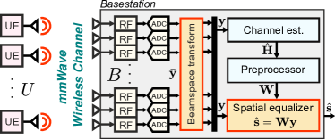
We consider the uplink of an all-digital mmWave massive MU-MIMO system as depicted in \freffig:system_overview. Here, single-antenna UEs transmit data to a basestation that is equipped with a -antenna uniform linear array. The antenna-domain received vector at the BS is given byaaaAlthough this model only holds for frequency-flat channels, an extension of this paper’s results to frequency-selective channels is straightforward if using orthogonal frequency-division multiplexing (OFDM). , where is the antenna-domain receive vector, is the antenna-domain MIMO channel matrix, contains the transmit symbols of the UEs (taken from a constellation set), and models noise with i.i.d. circularly symmetric complex Gaussian entries with variance . The transmit symbols are assumed to satisfy the power constraint .
II-B Beamspace System Model
Using the well-known planar-wave approximationbbbWe use the planar-wave approximation for mathematical analysis—our simulations, however, use channel vectors generated with spherical waves. [12], we model the wireless channel between a UE and the BS as
| (1) |
where refers to the number of propagation paths, is the complex-valued channel gain of the th path, and
| (2) |
where the spatial frequency is determined by the th path’s angle-of-arrival at the BS antenna array. Due to the predominantly directional nature of wave propagation at mmWave frequencies [13], is typically much smaller than in massive MIMO systems, meaning that the channel vector of each UE is a superposition of only a few complex sinusoids. Hence, the DFT of in \frefeq:planarwave results in an approximately sparse vector [10], meaning that most of its entries are close to zero, while only few entries have large magnitude. By applying such a spatial DFT to the antenna-domain received vector , we arrive at the following beamspace system model:
| (3) |
Here, is the beamspace receive vector, is the unitary DFT matrix, is the beamspace MIMO channel matrix, and is the beamspace-equivalent noise vector, which has the same statistics as as is unitary. Therefore, beamspace system model in \frefeq:BD_model is statistically equivalent to the antenna-domain system model, and data detection using both models gives exactly the same result.
II-C SParsity-ADaptive Equalization (SPADE)
We now summarize SPADE [8], which is the main ingredient of our ASIC. First, we note that due to the approximate sparsity of the beamspace channel matrix , the beamspace LMMSE equalization matrix also exhibits approximate sparsity. Second, since the beamspace receive vector is a linear combination of a few sparse vectors, it is also approximately sparse. SPADE exploits this approximate sparsity in both and in order to reduce the number of effective multiplications during equalization .
Consider the th inner product . Due to approximate sparsity of and the rows of , many of the operands and have small magnitude. Since the number of BS antennas is large in massive MIMO, each such inner product is a sum of a large number of products. Consequently, one can skip multiplications where both and are small, without a notable perturbation on the inner-product’s result. Noting that each complex-valued multiplication consists of four real-valued multiplications, instead of skipping an entire complex-valued multiplication, one can individually turn on or off the real-valued multiplications based on the absolute values of their operands. SPADE uses two thresholds and to skip real-valued multiplications for which the absolute value of both operands are below the respective thresholds. These thresholds trade computational complexity for accuracy of the inner product and are determined offline based on simulations with the goal of minimizing (i) the approximation error and (ii) the multiplier activity rate, which is the average number of executed real-valued multiplications divided by the total real-valued multiplications involved in .
Note that the rows of may have vastly different dynamic ranges, calling for a separate threshold for each row. In order to use the same threshold for all of the inner products, the rows of are scaled to obtain , where , and is a small constant that ensures that is just below one. The final symbol estimates are then obtained as . This row-wise scaling has the additional benefit of reducing the overall dynamic range of the entries in , thereby reducing the minimum required bitwidth of entries in in its fixed-point representation.
II-D Error-Rate Performance Simulations
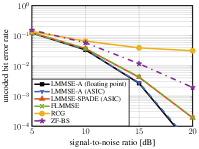
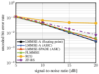
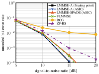
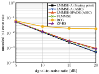
In order to evaluate the impact of SPADE’s approximate inner-product computations on the system performance, we simulate the uncoded bit error-rate (BER) for beamspace LMMSE employing SPADE (referred to as ‘LMMSE-SPADE’). \freffig:BER shows the results for LMMSE-SPADE with or UEs transmitting -QAM symbols to a -antenna BS over line-of-sight (LoS)cccThe generated LoS channel vectors also include reflective paths. and non-LoS channels generated with the QuadRiGa mmMAGIC simulator [14]. We also show the BER of the antenna-domain mode of our ASIC, labeled “LMMSE-A (ASIC),” as well as a floating-point reference. We observe that LMMSE-SPADE incurs less than dB and dB SNR loss at % BER for and , respectively, compared to LMMSE-A. The threshold pairs corresponding to these simulations and the ASIC measurements are detailed in \frefsec:threshols. Furthermore, we compare the BER to three state-of-the-art massive MU-MIMO data detection algorithms: FLMMSE [15], recursive conjugate gradient (RCG) [16], and zero-forcing with beam selection (ZF-BS) [6]. While FLMMSE exhibits similar performance to LMMSE-SPADE, RCG suffers a performance loss in highly correlated mmWave channels, and ZF-BS suffers a notable performance loss in non-LoS channels.
II-E How to Select the SPADE Thresholds?
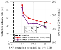
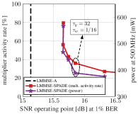
The SPADE thresholds and determine the inner-product accuracy and the multiplier activity rate. To simplify implementation and to eliminate the need for determining these thresholds on-the-fly for each considered system dimension and channel condition (LoS or non-LoS), we found a fixed pair of thresholds that achieves a desirable trade-off between BER and power savings. To this end, we performed BER simulations offline for a range of threshold pairs, and for each pair, we computed the average multiplier activity rate and the SNR operating point (i.e., the minimum SNR that achieves BER). \freffig:thresholds provides the results for a system with BS antennas and UEs, in which we also show the power consumption corresponding to each threshold pair, extracted from stimuli-based power simulations at MHz (on the right y-axis), as well as the chosen threshold pair. Evidently, the multiplier activity well-predicts the power consumption.
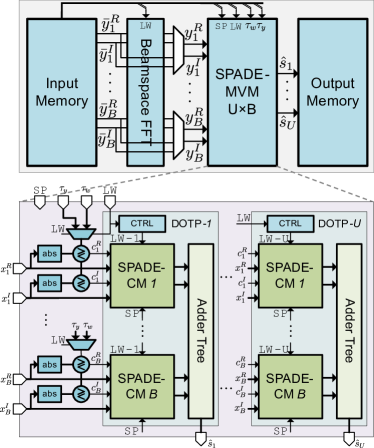
III VLSI Architecture
The high-level architecture of our ASIC is illustrated at the top of \freffig:top and consists of four main components: (i) an input SRAM, which stores input test vectors, (ii) a fast Fourier transform (FFT) unit that transforms the antenna-domain received vectors into beamspace, (iii) a SPADE-enabled matrix-vector multiplier (MVM), and (iv) an output SRAM that stores the results. The beamspace FFT is implemented using a fully-unrolled radix-4 architecture with low-resolution twiddle factors according to [17]; this enables transforming an entire -element antenna-domain vector into beamspace per clock cycle at a small area and power overhead. To compare the efficacy of beamspace vs. antenna-domain processing, our architecture can be configured to operate either in antenna-domain mode, in which the beamspace FFT is turned off, or in beamspace mode, in which the beamspace FFT is active. In addition, when operating in beamspace mode, a save-power (SP) signal controls whether SPADE-based power saving is activated; this enables us to measure the impact of SPADE.
| This work | [15] | [16] | [18] | [19] | [6] | ||
| Algorithm | LMMSE-SPADE | FLMMSE | RCG | MPD | LMMSE | ZF-BS | |
| System dimension | 64 16 | 32 16 | 128 8 | 128 32 | 128 8 | 128 16 | |
| Modulation [QAM] | 16 | 16 | 64 | 256 | 256 | 16 | |
| Channel scenario | LoS | NLoS | – 11footnotemark: 1 | – | – | – | – |
| Includes preprocessing | no | no | no | no | yes | yes | |
| Technology [nm] | 22 | 65 | 65 | 40 | 28 | 28 | |
| Core voltage [V] | 0.8 | 1.0 | 1.2 | 0.9 | 0.9 | – | |
| Core area [] | 2.3 22footnotemark: 2 | 2.41 | 1.6 | 0.58 | 0.12 | – | |
| Max. clock frequency [MHz] | 720 | 600 | 312 | 500 | 425 | 300 | 560 |
| Max. throughput [Gbps] 33footnotemark: 3 | 46 | 39 | 9.98 | 1.0 | 1.38 | 0.15 | 2.24 |
| Max. clock frequency [MHz] (FBB) 44footnotemark: 4 | 920 | 890 | – | – | – | 300 | – |
| Max. throughput [Gbps] 33footnotemark: 3 (FBB) | 58.8 | 54 | – | – | – | 0.15 | – |
| Power [mW] | 544 22footnotemark: 255footnotemark: 5 | 570 22footnotemark: 255footnotemark: 5 | 290 | 120 | 220.6 | 18 | 251 |
| Energy eff. [pJ/b] | 11.8 55footnotemark: 5 | 14.6 55footnotemark: 5 | 29 | 120 | 160 | 120 | 112 |
| Area eff. [Gbps/] | 20 55footnotemark: 5 | 17 55footnotemark: 5 | 4.15 | 0.63 | 2.38 | 1.25 | – |
| Norm. energy eff. [pJ/b] 66footnotemark: 677footnotemark: 7 | 11.8 | 14.6 | 12.6 | 36.1 | 34.6 | 148 | 69.5 |
| Norm. area eff. [Gbps/] 66footnotemark: 677footnotemark: 7 | 20 | 17 | 53 | 7.8 | 28.6 | 1.28 | – |
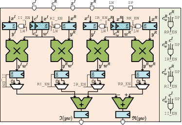
III-A SPADE-MVM Architecture
The top-level architecture of the SPADE-MVM is depicted at the bottom of \freffig:top and consists of dot-product (DOTP) modules, each consisting of SPADE complex-valued multipliers (CMs), whose internal architecture is shown in \freffig:spadecm, and a -input adder tree consisting of adder layers, with pipeline registers after every two layers. Each of the dot product modules computes one entry of . SPADE-MVM receives a -element complex-valued vector per clock cycle through its input ports. During a -cycle weight-loading phase, indicated by raising a load-weight (LW) signal, a new equalization matrix is loaded into the registers of the SPADE-CMs. When LW is low, the incoming vector is multiplied to the rows of the stored simultaneously, performing one equalization operation per clock cycle. Furthermore, if LW is asserted, the absolute value of the real and imaginary parts of the input signals are compared to the w-threshold and otherwise, they are compared to the y-threshold . The resulting comparison bits are broadcast to the SPADE-CMs, where they are used for adaptive power saving.
III-B SPADE-CM Architecture
fig:spadecm details the SPADE-CM architecture which contains four real-valued multipliers and two adders. The pipelining registers not only shorten the critical path and reduce glitching activity, but also provide a mechanism to conditionally mute each of the four real-valued multipliers by freezing their inputs. Two of the registers (cf. the hatched pattern in \freffig:spadecm) store the entries of the equalization matrix along with the w-threshold comparison bits ( and ). The other four input registers hold the real/imaginary parts of the input signal. If the save-power (SP) signal is asserted, and both the w- and y-threshold comparison bits corresponding to a particular register are set, then that register is disabled to mute switching activity, which reduces dynamic power consumption. At the input of the adders, the multiplexer selects zero if the preceding multiplier was muted. Depending on the channel conditions (e.g., depending on how sparse is) and the instantaneous receive vector, different subsets of multipliers within SPADE-CMs are muted; this results in adaptive savings in dynamic power.
IV ASIC Implementation Results
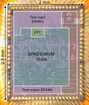
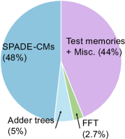
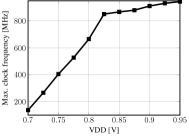
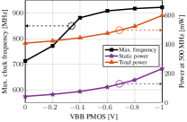
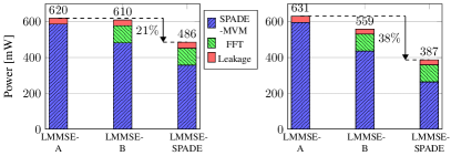
A micrograph of the fabricated ASIC along with an area breakdown is shown in \freffig:chip_micrograph. \freffig:vfs shows the impact of the core voltage (VDD) on the maximum clock frequency and \freffig:bb shows the effect of forward body biasing (FBB) on the maximum clock frequency and the power consumption at a clock frequency of MHz. For simplicity, in \freffig:bb, only the PMOS body biasing voltage is varied and the NMOS body bias is fixed to V. We observe that V of PMOS forward body biasing, results in a % increase in the maximum clock frequency and a % increase in the total power consumption, which is due to the increase in leakage power. \freffig:power_brk shows the power breakdown of our ASIC’s main modules in three modes: (i) LMMSE-A, in which the beamspace FFT is turned off and antenna-domain equalization is performed, (ii) LMMSE-B, in which beamspace equalization is performed but without SPADE-based power saving (no multiplications are muted), and (iii) LMMSE-SPADE, which performs beamspace equalization with SPADE-based power saving. LMMSE-SPADE provides % and % power savings with respect to LMMSE-A under non-LoS and LoS conditions, respectively.
tbl:copmarison compares the key characteristics of our fabricated ASIC with that of state-of-the-art massive MU-MIMO data detectors. We scale the reported metrics as detailed in footnotes and . Our ASIC achieves similar or superior normalized energy- and area-efficiency compared to state-of-the-art hardware implementations. Even though the designs in [16, 18] achieve competitive energy and area efficiency, their BER is inferior in mmWave channels (cf. \freffig:BER and [18]). The design from [15] achieves better area-efficiency by utilizing extremely low-resolution equalization weights and input vectors. This design, however, would require a more complicated preprocessing engine than our design. Finally, we emphasize that our ASIC achieves up to Gbps at only mW with body biasing, which is, to our knowledge, the highest 16-QAM throughput reported in the literature.
V Conclusions
We have presented the first architecture and ASIC of a mmWave massive MU-MIMO equalizer capable of both antenna-domain and beamspace equalization with adaptive power-saving capabilities. In beamspace equalization mode, our ASIC is able to use SPADE [8] to adaptively reduce the dynamic power consumption. Measurement results have revealed that, despite the overhead of the necessary beamspace FFT, beamspace equalization with SPADE enables up to % power savings compared to antenna-domain equalization. Furthermore, our ASIC achieves a record throughput of Gb/s with body biasing at a better or similar normalized energy- and area-efficiency compared to state-of-the-art designs.
References
- [1] 3GPP, “5G; NR; base station (BS) radio transmission and reception,” Apr. 2022, TS 38.104 version 16.11.0 Rel. 16.
- [2] Ericsson, “Meeting 5G network requirements with massive MIMO,” White Paper, Feb. 2022.
- [3] T. S. Rappaport, R. W. Heath Jr., R. C. Daniels, and J. N. Murdock, Millimeter Wave Wireless Communications. Prentice Hall, 2015.
- [4] P. Schniter and A. Sayeed, “Channel estimation and precoder design for millimeter-wave communications: The sparse way,” in Proc. Asilomar Conf. Signals, Syst., Comput., Nov. 2014, pp. 273–277.
- [5] M. Abdelghany, U. Madhow, and A. Tölli, “Beamspace local LMMSE: An efficient digital backend for mmWave massive MIMO,” in Proc. IEEE Int. Workshop Signal Process. Advances Wireless Commun. (SPAWC), Aug. 2019, pp. 1–5.
- [6] M. Mahdavi, O. Edfors, V. Öwall, and L. Liu, “Angular-domain massive MIMO detection: Algorithm, implementation, and design tradeoffs,” IEEE Trans. Circuits Syst. I, vol. 67, no. 6, pp. 1948–1961, Jan. 2020.
- [7] S. H. Mirfarshbafan and C. Studer, “Sparse beamspace equalization for massive MU-MIMO mmWave systems,” in Proc. IEEE Int. Conf. Acoust., Speech, Signal Process. (ICASSP), May 2020, pp. 1773–1777.
- [8] S. H. Mirfarshbafan and C. Studer, “SPADE: Sparsity-Adaptive Equalization for MMwave massive MU-MIMO,” in Proc. IEEE Workshop Stat. Signal Process. (SSP), Aug. 2021, pp. 211–215.
- [9] E. Gönültaş, S. Taner, A. Gallyas-Sanhueza, S. H. Mirfarshbafan, and C. Studer, “Hardware-aware beamspace precoding for all-digital mmWave massive MU-MIMO,” IEEE Commun. Lett., vol. 25, no. 11, pp. 3709–3713, Aug. 2021.
- [10] S. H. Mirfarshbafan, A. Gallyas-Sanhueza, R. Ghods, and C. Studer, “Beamspace channel estimation for massive MIMO mmWave systems: Algorithm and VLSI design,” IEEE Trans. Circuits Syst. I, pp. 1–14, Sep. 2020.
- [11] D. Seethaler and H. Bölcskei, “Performance and complexity analysis of infinity-norm sphere-decoding,” IEEE Trans. Inf. Theory, vol. 56, no. 3, pp. 1085–1105, Mar. 2010.
- [12] D. Tse and P. Viswanath, Fundamentals of Wireless Communication. Cambridge Univ. Press, 2005.
- [13] H. Miao, J. Zhang, P. Tang, L. Tian, X. Zhao, B. Guo, and G. Liu, “Sub-6 GHz to mmWave for 5G-advanced and beyond: Channel measurements, characteristics and impact on system performance,” IEEE J. Sel. Areas Commun., vol. 41, no. 6, pp. 1945–1960, May 2023.
- [14] S. Jaeckel, L. Raschkowski, K. Börner, L. Thiele, F. Burkhardt, and E. Eberlein, “QuaDRiGa - quasi deterministic radio channel generator user manual and documentation,” Fraunhofer Heinrich Hertz Institute, Tech. Rep. v2.0.0, Aug. 2017.
- [15] O. Castañeda, Z. Boynton, S. H. Mirfarshbafan, S. Huang, J. C. Ye, A. Molnar, and C. Studer, “A resolution-adaptive 8 mm2 9.98 Gb/s 39.7 pJ/b 32-antenna all-digital spatial equalizer for mmWave massive MU-MIMO in 65nm CMOS,” in Proc. IEEE Eur. Solid-State Circuits Conf. (ESSCIRC), Sep. 2021.
- [16] L. Liu, G. Peng, P. Wang, S. Zhou, Q. Wei, S. Yin, and S. Wei, “Energy- and area-efficient recursive-conjugate-gradient-based MMSE detector for massive MIMO systems,” IEEE Trans. Signal Process., vol. 68, pp. 573–588, Jan. 2020.
- [17] S. H. Mirfarshbafan, S. Taner, and C. Studer, “SMUL-FFT: a streaming multiplierless fast Fourier transform,” IEEE Trans. Circuits Syst. II, vol. 68, no. 5, pp. 1715–1719, Mar. 2021.
- [18] W. Tang, C.-H. Chen, and Z. Zhang, “A 0.58-mm2 2.76-Gb/s 79.8-pJ/b 256-QAM message-passing detector for a 128 × 32 massive MIMO uplink system,” IEEE J. Solid-State Circuits, vol. 56, no. 6, pp. 1722–1731, Apr. 2021.
- [19] H. Prabhu, J. N. Rodrigues, L. Liu, and O. Edfors, “A 60pJ/b 300Mb/s 128×8 massive MIMO precoder-detector in 28nm FD-SOI,” in IEEE Int. Solid-State Circuits Conf. (ISSCC) Dig. Tech. Papers, Mar. 2017, pp. 60–61.
- [20] J. M. Rabaey, A. Chandrakasan, and B. Nikolić, Digital integrated circuits: A design perspective. Prentice Hall, 2003.