Edge-state transport in twisted bilayer graphene
Abstract
We investigate the electronic structure and transport properties of twisted bilayer graphene (TBLG) at a twist angle of . Using a combination of molecular dynamics and tight-binding calculations, we find two superlattice gaps in the energy spectrum of the bulk, which emerge close to the Fermi level from the atomic rearrangement of the carbon atoms leading to a corrugation of the graphene sheets. Nanoribbons made from 1.696°-TBLG show edge-localized states inside the superlattice gaps. Applying the Green’s function method, we demonstrate that the edge states carry electronic current with conductance values close to the conductance quantum. The edge states can generate a non-local resistance, which is not due to one-way transport at the edges but due to the fact that these states are localized only at certain edges of the system, depending on how the nanoribbon has been cut from the bulk.
I Introduction
Graphene paved the way for the emergence of 2D materials almost two decades ago [1], so it is not surprising that the graphene bilayer is doing the same for stacked structures made of 2D materials. Bilayer graphene (BLG) comes in two semi-metallic flavors, one with a parabolic low-energy dispersion [2, 3, 4] in its most common and stable phase known as AB or Bernal stacking, and one with displaced Dirac cones in the less common and energetically unfavorable AA stacking phase [5, 6, 7]. In general, BLG exhibits both excellent electrical and thermal conductivity at room temperature [8, 9], mechanical stiffness, strength and flexibility [10, 11], high transparency [12] and allows the tuning of its electrical properties via external gating and doping [13, 14, 15, 16, 17].
In recent years, introducing a twist angle between two stacked graphene layers has enabled an extraordinary array of physical phenomena not present in neither graphene nor BLG [18]. The twist angle generates what is called a Moiré pattern (see Figure 1), an alternating distribution of stacking zones that alters the way the monolayers interact with each other [19, 20, 21]. This interaction has been shown to lead to strongly correlated electronic behavior such as unconventional superconductivity and Mott-like insulating states [22, 23]. With twisted bilayer graphene (TBLG) at the forefront, the field of twistronics has emerged as a highly fertile research ground with promising technological applications [24].
One distinct feature of these TBLG systems is how the twist angle affects both the atomic arrangement and the electronic structure. It has been shown that an atomic reconstruction is energetically favorable for TBLG leading to a corrugation of the layers [25, 26, 27], which is particularly steep for twist angles below 5°, whereas for angles above 15° the monolayers remain essentially flat. For certain small angles, the atomic reconstruction even leads to the creation of band gaps, named also superlattice gaps [28, 29]. Graphene’s dispersion remains linear for most twist angles [30, 31, 32] and the van Hove singularities in its density of states are shifted towards energies which are accessible through gating [19, 33, 34]. Furthermore, ”magic” angles lead to the existence of flat bands where electrons are tightly packed in momentum space and correlation effects become important. Most of the research is focused on this magic angle TBLG, both theoretically [35, 31, 36, 37] and experimentally [22, 23, 38]. However, interesting phenomena exist for many twist angles [39, 29, 40].
Edge states in TBLG have attracted some attention. It has been demonstrated experimentally that the zigzag edge states of graphene can be tuned by stacking two zigzag nanoribbons with a twist [41]. In magic angle TBLG edge states can give rise to ferromagnetism and the anomalous Hall effect [42]. A variety of edge states were calculated in TBLG nanoribbons that reside amid other electronic states [43] and it has been shown that the mechanical sliding of one layer in TBLG causes the migration of edge states in the energy spectrum [44]. Particularly important for this article are transport measurements by Ma et al. showing a non-local resistance in a TBLG device with a twist of 1.68°, which they attribute to the existence of counter-propagating edge states within the superlattice gaps [45].
In this paper, we aim to shed light on these edge states. We investigate TBLG at a twist angle of – named in the following 1.696°-TBLG – by using a combination of molecular dynamics (MD) and tight-binding (TB) methodologies. We find two superlattice gaps in the electronic structure of the bulk, which are due to the atomic reconstruction of the carbon atoms that lead to a corrugation of the graphene layers. In the case of nanoribbons made from 1.696°-TBLG, edge localized states reside inside these gaps. The nonequilibrium Green’s function (NEGF) method is applied to the MD+TB model to study the current flow in a 1.696°-TBLG device. We find that the edge states carry current with conductance values close to the conductance quantum and can lead to a nonlocal resistance. However, the edge states are bi-directional and the non-local resistance is due to the fact that the edge states are localized only at certain edges of the system, depending on how the nanoribbon is cut from the bulk.
II System & Methods
II.1 TBLG unit cell
In order to construct the TBLG systems, we start with a graphene monolayer with lattice vectors and , where is the carbon-carbon distance. The atomic base consists of carbon atoms at positions and . A Moiré pattern will emerge by taking two graphene layers, separated vertically by , and rotating them by the twist angle
| (1) |
The positive integers and will identify a given TBLG system and define the pair of superlattice vectors and .
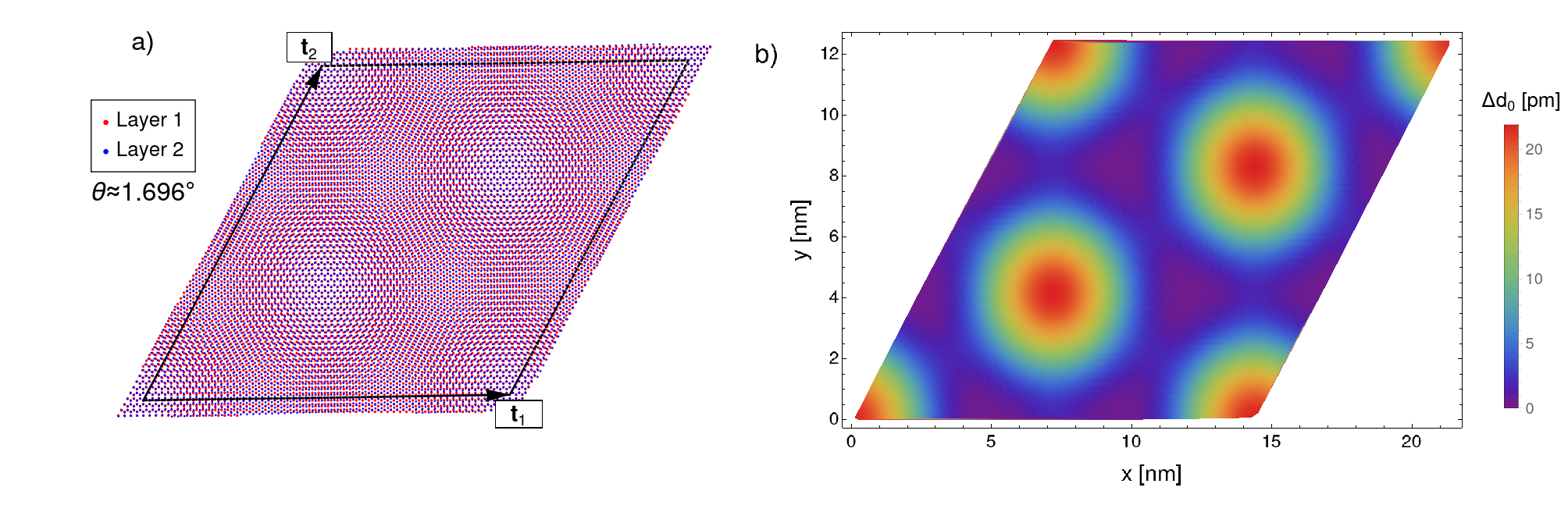
Figure 1 (a) shows a TBLG system constructed by this method. The system has a twist angle of , corresponding to the pair of integers and . The new supercell, defined by the dashed parallelogram, contains a pattern of alternating stacking areas. The AA stacking is visible where carbon sites of one layer are directly above carbon sites of the other layer while the AB stacking can be seen where hexagons of one layer enclose a carbon site from the other layer. The continuous modulation of these stacking zones creates the Moiré pattern. Systems constructed from this particular TBLG supercell, containing 13,392 carbon atoms, will be the main focus of this article.
II.2 Structural relaxation
Two methods are typically used for the structural relaxation of the TBLG system. Density Functional Theory (DFT) calculations are accurate but computationally demanding and thus, limited to large twist angles where the supercell is rather small [46]. Because MD calculations are able to handle hundreds of thousands of atoms and correctly reproduce the corrugation of the graphene layers [25, 27, 47], we perform structural relaxation calculations on the TBLG supercell via the LAMMPS MD code [48, 49]. The interlayer REBO [50, 51] potential and the intralayer Kolmogorov-Crespi [52] potential are employed since they are tailored to graphitic and misalinged graphene layered systems, respectively. The new relaxed structure of the 1.696°-TBLG supercell (see Figure 1 (b)) will be utilized for the remainder of the article.
II.3 Tight-Binding model
Effective models and low energy approximations are able to reproduce key features of the electronic structure of TBLG bulk systems [30, 53, 54, 35], such as the renormalization of the Fermi velocity and flat bands. However, we are interested not only in bulk systems but also in nanoribbons and devices and choose for the TBLG system the TB Hamiltonian
| (2) |
where indicates the atomic state localized on the carbon atom at . The coupling term between sites is determined by the Slater-Koster formula [55]
| (3) |
where is the direction cosine of along the direction. The Slater-Koster parameters are defined as
| (4) |
with the tight-binding parameters [56]
| (5) |
II.4 Nonequilibrium Green’s funcion method
The NEGF method is applied to study the electrical transport in the TBLG devices and here, we briefly summarize the essential equations [57, 58, 59]. The Green’s function of the system is given by
| (6) |
where is the energy of the injected electrons and is the tight-binding Hamiltonian (2). The contacts are modeled by the so-called wide-band model implying for these a constant energy-independent surface density of states. It is taken into account in the Green’s function by means of the self-energies , where the sum runs over the carbon atoms attached to the contact .
The transmission between a pair of contacts, and , is given by
| (7) |
where the inscattering function associated to contact is defined as . The transmission determines the conductance for electrons of energy between the selected pair of contacts, . Furthermore, the local current flowing between the atoms and can be calculated with [60, 61]
| (8) |
Finally, for the non-local resistance calculations we consider 4 contacts in the device, where electrons are injected by the S contact, collected in the D contact and the voltage between a pair of contacts A and B is calculated. The non-local resistance is calculated as follows
| (9) |
where
| (10) |
For more details on the derivation of (9) and (10) in the context of the NEGF method, see our previous work [39].
III Band structure calculations
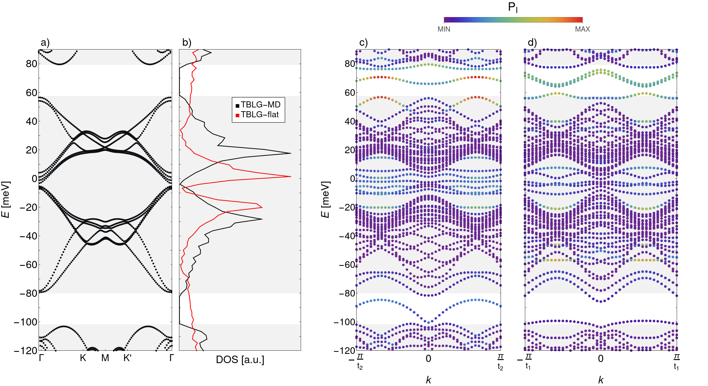
We perform the MD+TB calculation to obtain the electronic structure of the 1.696°-TBLG bulk system, shown in Figure 2 (a,b). Two band gaps with a size of about 20 meV, highlighted by the white shaded regions, are found. The DOS, which is calculated over the full Brillouin zone, confirms these gaps. We have included also the DOS of a flat system, where MD calculations were not performed and no energy gaps are found. Hence, the energy gaps in Figure 2 (a) and (b) originate from the atomic reconstruction of the system at such a small twist angle and we will refer to them as superlattice gaps for the remainder of the article. Note that two van Hove singularities are present at low energies, a fingerprint of the TBLG systems. Also note that given the TBLG supercell used for the calculations, see Figure 1, the Brillouin Zone is folded and the Dirac crossing is moved from the and points to .
With the bulk energy bands as a reference point, we turn our attention to the energy landscape of nanoribbons. Figure 2 (c) and (d) show the energy bands of two 1.696°-TBLG nanoribbons, both with a width of 4 supercells and a total of atoms each. Nanoribbon (c) is periodic in the direction of vector while nanoribbon (d) is periodic in the direction of . We find for these nanoribbons states inside the superlattice gaps. The color of the energy bands gives the inverse participation ratio at each () value [62] and unveils the localization of the states in the superlattice gaps. Note that these states exist for both directions of the nanoribbon though the number of the states change.
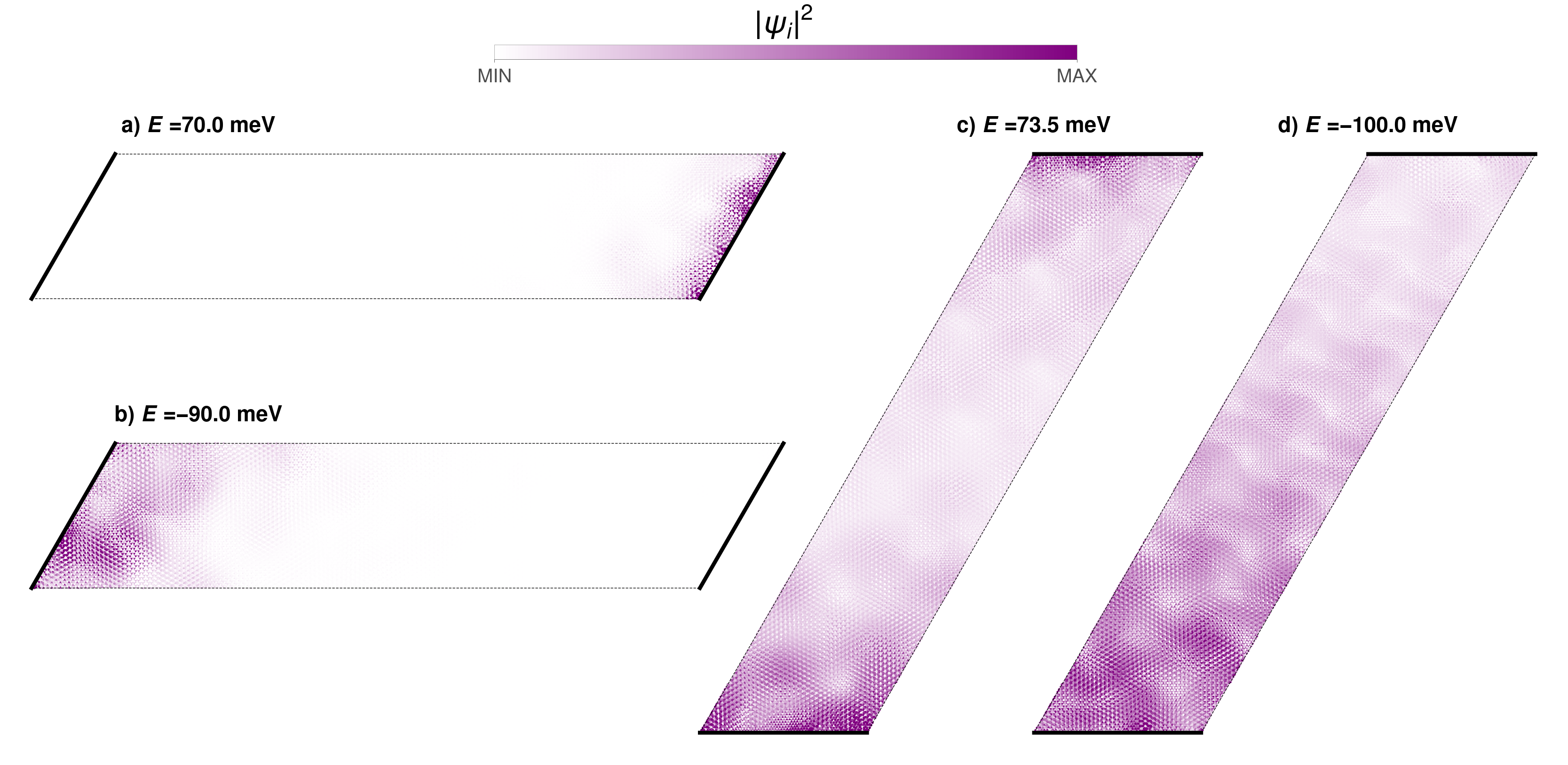
The spatial distribution of the states inside the superlattice gaps of the 1.696°-TBLG nanoribbons are shown in Figure 3. Solid thick lines indicate the edges of the nanoribbons, while dashed thin lines mark their periodic directions; panels (a,b) correspond to the nanoribbon periodic in the direction, while (c,d) are for the nanoribbon with periodicity in the direction. The states in (a-c) are localized predominantly at the edges of the nanoribbon. States in (a,b) are limited exclusively to one edge, while the state in (c) is present at both edges. The state in (d) is included as a contrast showing a largely delocalized state. Note that in general the observed localization (and delocalization) of the eigenstates is in line with the values of the inverse participation ratio in Figure 2 (c,d), since the higher the value of the smaller the spatial extension of the state and vice-versa.
So far, our MD+TB calculations performed on 1.696°-TBLG systems confirm the emergence of superlattice gaps due to the corrugation of the graphene layers. Furthermore, inside these superlattice gaps we find localized states at the edges of the nanoribbons. These results are in agreement with the findings in [45]. Next, we explore the transport properties of these edge localized states.
IV Electronic transport
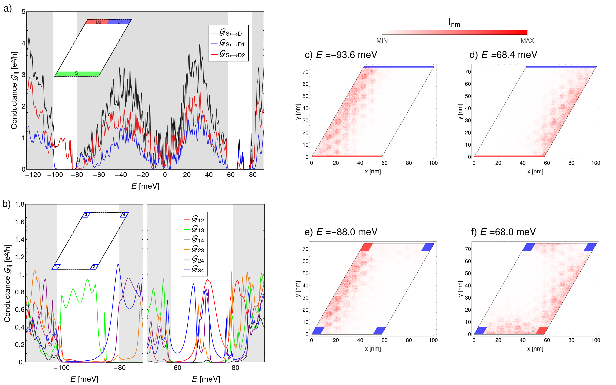
We now turn our attention to the transport properties of the edge localized states inside the superlattice gaps. Figure 4 (a) and (b) show the conductance as a function of the electron energy for a 1.696°-TBLG device consisting of supercells. The contact positions are sketched in the insets. As in Figure 2, the background shading highlights the superlattice gaps and helps to identify transport in those. In panel (a) we observe transport inside the superlattice gaps with conductance values close to the conductance quantum . We can also observe that the current is collected mainly, either by the left or right part of the drain contact, or , depending on the superlattice gap. In panel (b) the contacts are placed at the corners of the nanoribbon, which allows to identify transport at all edges. Again, we observe that the current inside the superlattice gaps is carried predominantly along the edges, while the transport across the device, and , is heavily suppressed. Panels (c-f) show the local current flow at certain electron energies and confirm the localization of the current on the edges of the system. This observation is in-line with the localization of the eigenstates shown in Figure 3. Importantly, we have verified in all our transport calculations that the edge states carry the current equally in both direction, , which is in agreement with the fact that time-reversal symmetry is preserved.
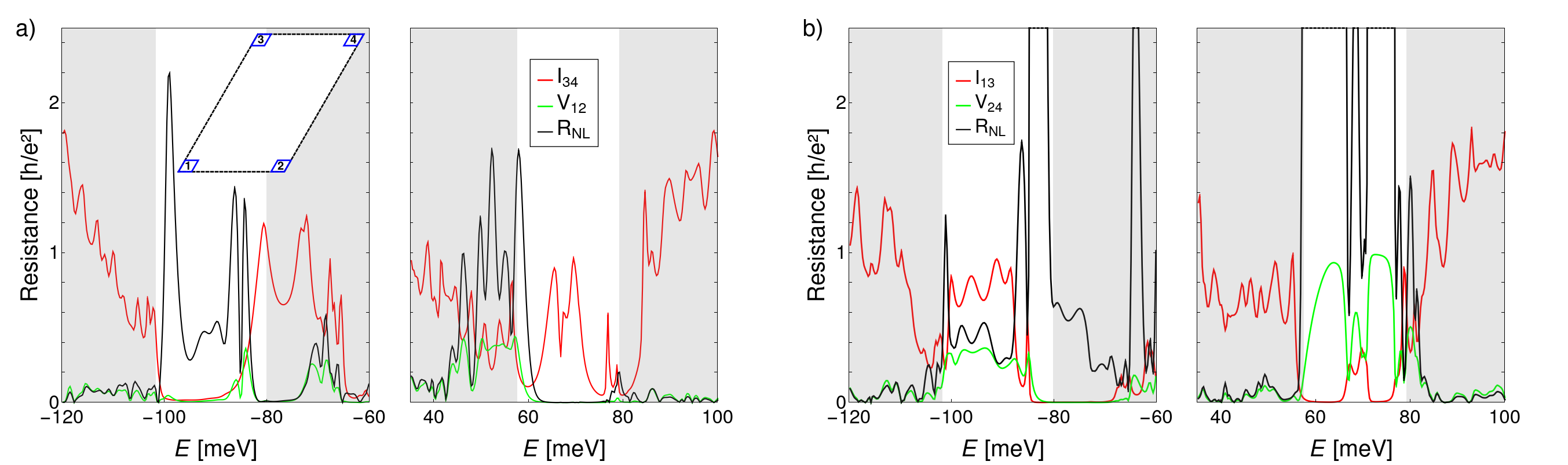
Next, we analyze in Figure 5 the non-local resistance of the 1.696°-TBLG device, consisting of supercells with 4 contacts. For that, the current flow is calculated between two contacts on one edge of the system, while the voltage drop is determined between two contacts on the opposite edge. The nonlocal resistance is defined as the quotient of these two quantities. In Figure 5, we show the voltage, current and the non-local resistance for two different contact wirings; in panel (a) the measurements are along the direction while in (b) they are in the direction. Both panels show within the superlattice gap a non-local resistance but the value of the resistance depends strongly on the wiring of the contacts. While in panel (a) values in the range of the resistance quantum are observed, the values in panel (b) can be extremely large. These large values can be explained by the fact that a voltage drop is detected between the contacts (green curves) but the current flowing though the device is almost zero (red curves). In the upper superlattice gap of panel (a), the non-local resistance extends partially to the region outside the gap, which can be understood by means of Figure 2 showing that localized edge states appear also outside the gap. We find in Figure 5 clear evidence for a nonlocal resistance inside the superlattice gap. However, we point out again that the transport along the edge states is bidirectional and the non-local resistance is due to the fact that the edge states are localized only on certain edges of the device, which will be discussed in the following.
V Nanoribbon edge termination
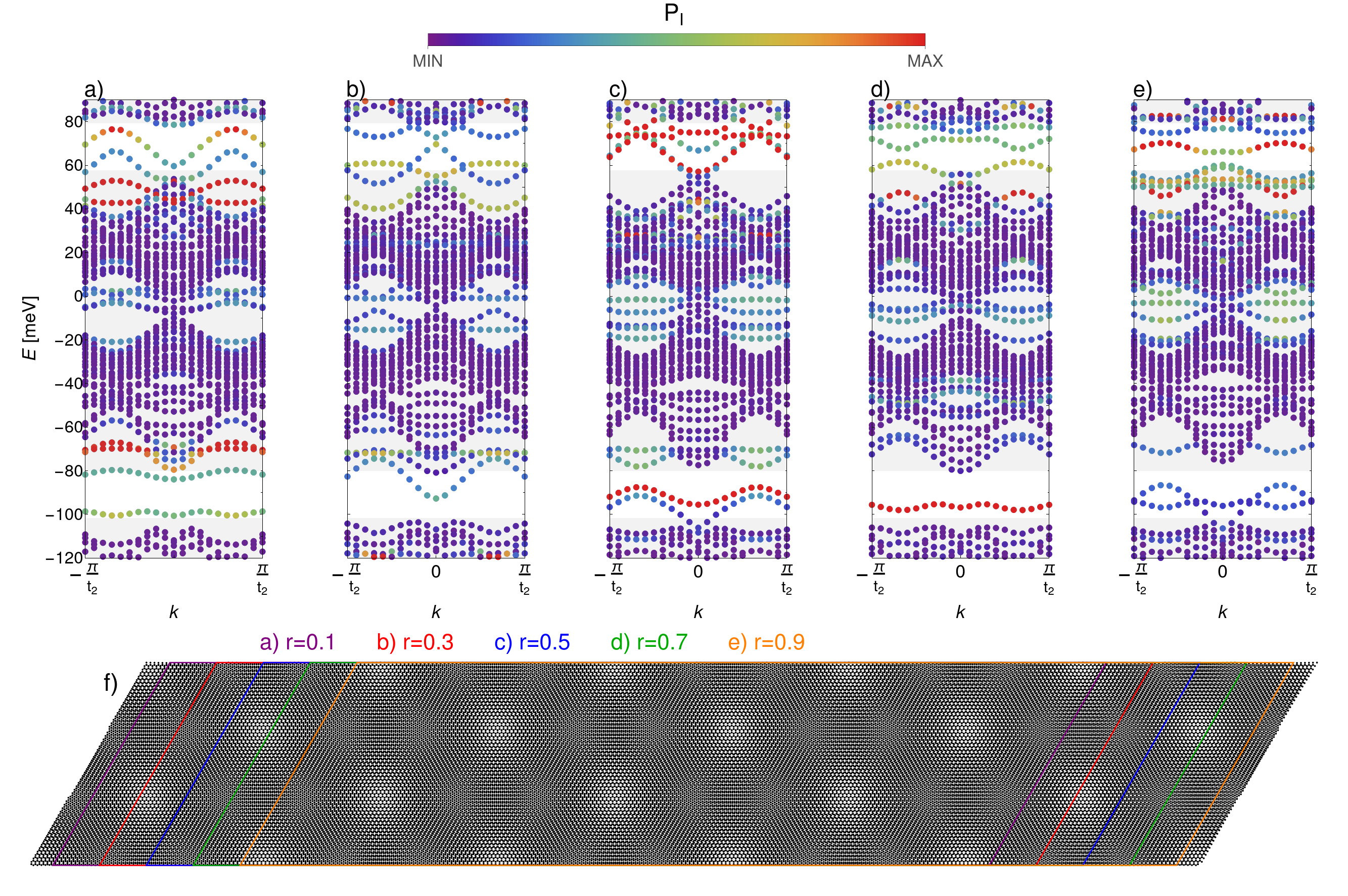
We are left to understand the localization of the edge states at only certain edges of the system. In Figure 2 (c,d), we analyzed the band structure of 1.696°-TBLG nanoribbons with a width of 4 unit cells and periodicity in the directions and , respectively. These two nanoribbons showed differences in the number and position of edge localized states. Here, we examine the effect of the edge termination of the nanoribbon on its electronic structure. Figure 6 shows how we construct the different versions of the nanoribbon by sliding a 4 unit cell wide ”cookie cutter” over a nanoribbon with a width of 5 unit cells and periodicity in the direction. The sliding of the ”cookie cutter” is given by , with . In this way, the 1.696°-TBLG nanoribbon with a width of 4 unit cells is conserved but the edge termination changes. The case of corresponds for the already studied nanoribbon of Figure 2 (c). Band structures for each nanoribbon are shown in Figure 6 (a-e). The band structures show that the unlocalized (purple) bands remain essentially unchanged as we change the edges. In contrast, localized states enter and exit the superlattice gaps as the edge termination is modified. This migration of localized states in and out of the superlattice gaps is very akin to the results found in [44]. Regardless of the nanoribbon termination, Figure 6 shows that one can expect a varying number of localized states inside the superlattice gaps of 1.696°-TBLG nanoribbons. When analyzing by eye the supercell shown in Figure 1 one could argue that it may be identical to a supercell rotated by 180°. While this is true for the approximate position of the AA and AB stacking zones, this symmetry does not hold on the microscopic level of individual atoms and therefore, permits edge states only at certain edges.
VI Conclusions
In this article, we have used a combination of TB, MD, and NEGF methodologies to investigate the electronic structure and transport properties of TBLG systems with a twist angle of . Our calculations show that two superlattice gaps emerge in the energy bands of the bulk, see Figure 2 (a), as a result of the atomic reconstruction that the system undergoes at small twist angles in order to minimize its energy. Using the relaxed supercell to build nanoribbons, Figure 2 (b,c) show that states appear inside the superlattice gaps of the bulk. These states are localized predominately at the edges of the nanoribbons; see Figure 3 (a-c). The edge localized states are dispersive and thus, able to carry electronic current as demonstrated by conductance and current density calculations for a device consisting of supercells (see Figure 4). A non-local resistance is found within the superlattice gaps, though its magnitude depends on the contact wiring, see Figure 5. This non-local resistance, observed experimentally by Ma et al. [45], is not due to one-way transport at the edges but due to the fact that the edge states are localized only at certain edges of the system. Finally, in Figure 6, we demonstrate how different edge terminations of the nanoribbon lead to the appearance and disappearance of edge localized states across the superlattice gaps. Therefore, the edge states in -TBLG are not topological (in the sense of a bulk-boundary correspondence) but rather have the character of current-carrying states that are induced by edge disorder.
VII Acknowledgments
We thank L.E.F. Foa-Torres for useful discussions and comments. We also thank L. Brendel for his help with the LAMMPS code. JAS-S gratefully acknowledges a CONAHCYT graduate scholarship. MN-E acknowledges support from Subprograma 127-FQ, UNAM. We gratefully acknowledge funding from CONAHCYT Frontera 428214, UNAM-PAPIIT IN103922, UNAM-PAPIIT IA106021 and PAIP-FQ(UNAM) 5000-9173.
References
- Novoselov et al. [2004] K. S. Novoselov, A. K. Geim, S. V. Morozov, D.-e. Jiang, Y. Zhang, S. V. Dubonos, I. V. Grigorieva, and A. A. Firsov, Electric field effect in atomically thin carbon films, science 306, 666 (2004).
- McCann and Koshino [2013] E. McCann and M. Koshino, The electronic properties of bilayer graphene, Reports on Progress in physics 76, 056503 (2013).
- Novoselov et al. [2006] K. S. Novoselov, E. McCann, S. Morozov, V. I. Fal’ko, M. Katsnelson, U. Zeitler, D. Jiang, F. Schedin, and A. Geim, Unconventional quantum hall effect and berry’s phase of 2 in bilayer graphene, Nature physics 2, 177 (2006).
- Katsnelson et al. [2006] M. Katsnelson, K. Novoselov, and A. Geim, Chiral tunnelling and the klein paradox in graphene, Nature physics 2, 620 (2006).
- Berashevich and Chakraborty [2011] J. Berashevich and T. Chakraborty, Interlayer repulsion and decoupling effects in stacked turbostratic graphene flakes, Physical Review B 84, 033403 (2011).
- Rakhmanov et al. [2012] A. Rakhmanov, A. Rozhkov, A. Sboychakov, and F. Nori, Instabilities of the a a-stacked graphene bilayer, Physical Review Letters 109, 206801 (2012).
- Roy et al. [1998] H.-V. Roy, C. Kallinger, and K. Sattler, Study of single and multiple foldings of graphitic sheets, Surface science 407, 1 (1998).
- Dean et al. [2010] C. R. Dean, A. F. Young, I. Meric, C. Lee, L. Wang, S. Sorgenfrei, K. Watanabe, T. Taniguchi, P. Kim, K. L. Shepard, et al., Boron nitride substrates for high-quality graphene electronics, Nature nanotechnology 5, 722 (2010).
- Ghosh et al. [2010] S. Ghosh, W. Bao, D. L. Nika, S. Subrina, E. P. Pokatilov, C. N. Lau, and A. A. Balandin, Dimensional crossover of thermal transport in few-layer graphene, Nature materials 9, 555 (2010).
- Neek-Amal and Peeters [2010] M. Neek-Amal and F. Peeters, Nanoindentation of a circular sheet of bilayer graphene, Physical Review B 81, 235421 (2010).
- Zhang et al. [2011] Y. Zhang, C. Wang, Y. Cheng, and Y. Xiang, Mechanical properties of bilayer graphene sheets coupled by sp3 bonding, Carbon 49, 4511 (2011).
- Nair et al. [2008] R. R. Nair, P. Blake, A. N. Grigorenko, K. S. Novoselov, T. J. Booth, T. Stauber, N. M. Peres, and A. K. Geim, Fine structure constant defines visual transparency of graphene, Science 320, 1308 (2008).
- Ohta et al. [2006] T. Ohta, A. Bostwick, T. Seyller, K. Horn, and E. Rotenberg, Controlling the electronic structure of bilayer graphene, Science 313, 951 (2006).
- McCann [2006] E. McCann, Asymmetry gap in the electronic band structure of bilayer graphene, Physical Review B 74, 161403 (2006).
- Castro et al. [2007] E. V. Castro, K. Novoselov, S. Morozov, N. Peres, J. L. Dos Santos, J. Nilsson, F. Guinea, A. Geim, and A. C. Neto, Biased bilayer graphene: semiconductor with a gap tunable by the electric field effect, Physical review letters 99, 216802 (2007).
- Oostinga et al. [2008] J. B. Oostinga, H. B. Heersche, X. Liu, A. F. Morpurgo, and L. M. Vandersypen, Gate-induced insulating state in bilayer graphene devices, Nature materials 7, 151 (2008).
- [17] G. G. Naumis, S. A. Herrera, S. P. Poudel, H. Nakamura, and S. Barraza-Lopez, Mechanical, electronic, optical, piezoelectric and ferroic properties of strained graphene and other strained monolayers and multilayers: An update, Rep. Prog. Phys 87, 016502.
- Andrei and MacDonald [2020] E. Y. Andrei and A. H. MacDonald, Graphene bilayers with a twist, Nature materials 19, 1265 (2020).
- Brihuega et al. [2012] I. Brihuega, P. Mallet, H. González-Herrero, G. T. De Laissardière, M. Ugeda, L. Magaud, J. Gómez-Rodríguez, F. Ynduráin, and J.-Y. Veuillen, Unraveling the intrinsic and robust nature of van hove singularities in twisted bilayer graphene by scanning tunneling microscopy and theoretical analysis, Physical review letters 109, 196802 (2012).
- Cisternas and Correa [2012] E. Cisternas and J. Correa, Theoretical reproduction of superstructures revealed by stm on bilayer graphene, Chemical Physics 409, 74 (2012).
- Varchon et al. [2008] F. Varchon, P. Mallet, L. Magaud, and J.-Y. Veuillen, Rotational disorder in few-layer graphene films on 6 h- si c (000- 1): A scanning tunneling microscopy study, Physical Review B 77, 165415 (2008).
- Cao et al. [2018a] Y. Cao, V. Fatemi, A. Demir, S. Fang, S. L. Tomarken, J. Y. Luo, J. D. Sanchez-Yamagishi, K. Watanabe, T. Taniguchi, E. Kaxiras, et al., Correlated insulator behaviour at half-filling in magic-angle graphene superlattices, Nature 556, 80 (2018a).
- Cao et al. [2018b] Y. Cao, V. Fatemi, S. Fang, K. Watanabe, T. Taniguchi, E. Kaxiras, and P. Jarillo-Herrero, Unconventional superconductivity in magic-angle graphene superlattices, Nature 556, 43 (2018b).
- Lau et al. [2022] C. N. Lau, M. W. Bockrath, K. F. Mak, and F. Zhang, Reproducibility in the fabrication and physics of moiré materials, Nature 602, 41 (2022).
- Gargiulo and Yazyev [2017] F. Gargiulo and O. V. Yazyev, Structural and electronic transformation in low-angle twisted bilayer graphene, 2D Materials 5, 015019 (2017).
- Uchida et al. [2014] K. Uchida, S. Furuya, J.-I. Iwata, and A. Oshiyama, Atomic corrugation and electron localization due to moiré patterns in twisted bilayer graphenes, Physical Review B 90, 155451 (2014).
- Jain et al. [2016] S. K. Jain, V. Juričić, and G. T. Barkema, Structure of twisted and buckled bilayer graphene, 2D Materials 4, 015018 (2016).
- Liu et al. [2021] B. Liu, L. Xian, H. Mu, G. Zhao, Z. Liu, A. Rubio, and Z. Wang, Higher-order band topology in twisted moiré superlattice, Physical Review Letters 126, 066401 (2021).
- Fortin-Deschênes et al. [2022] M. Fortin-Deschênes, R. Pu, Y.-F. Zhou, C. Ma, P. Cheung, K. Watanabe, T. Taniguchi, F. Zhang, X. Du, and F. Xia, Uncovering topological edge states in twisted bilayer graphene, Nano Letters 22, 6186 (2022).
- Dos Santos et al. [2007] J. L. Dos Santos, N. Peres, and A. C. Neto, Graphene bilayer with a twist: electronic structure, Physical review letters 99, 256802 (2007).
- Morell et al. [2010] E. S. Morell, J. Correa, P. Vargas, M. Pacheco, and Z. Barticevic, Flat bands in slightly twisted bilayer graphene: Tight-binding calculations, Physical Review B 82, 121407 (2010).
- Hass et al. [2008] J. Hass, F. Varchon, J.-E. Millan-Otoya, M. Sprinkle, N. Sharma, W. A. de Heer, C. Berger, P. N. First, L. Magaud, and E. H. Conrad, Why multilayer graphene on 4 h- sic (000 1) behaves like a single sheet of graphene, Physical review letters 100, 125504 (2008).
- Moon and Koshino [2013] P. Moon and M. Koshino, Optical absorption in twisted bilayer graphene, Physical Review B 87, 205404 (2013).
- Li et al. [2010] G. Li, A. Luican, J. Lopes dos Santos, A. Castro Neto, A. Reina, J. Kong, and E. Andrei, Observation of van hove singularities in twisted graphene layers, Nature physics 6, 109 (2010).
- Bistritzer and MacDonald [2011] R. Bistritzer and A. H. MacDonald, Moiré bands in twisted double-layer graphene, Proceedings of the National Academy of Sciences 108, 12233 (2011).
- Naumis et al. [2021] G. G. Naumis, L. A. Navarro-Labastida, E. Aguilar-Méndez, and A. Espinosa-Champo, Reduction of the twisted bilayer graphene chiral hamiltonian into a 2 2 matrix operator and physical origin of flat bands at magic angles, Physical Review B 103, 245418 (2021).
- Navarro-Labastida et al. [2022] L. A. Navarro-Labastida, A. Espinosa-Champo, E. Aguilar-Mendez, and G. G. Naumis, Why the first magic-angle is different from others in twisted graphene bilayers: Interlayer currents, kinetic and confinement energy, and wave-function localization, Physical Review B 105, 115434 (2022).
- Lisi et al. [2021] S. Lisi, X. Lu, T. Benschop, T. A. de Jong, P. Stepanov, J. R. Duran, F. Margot, I. Cucchi, E. Cappelli, A. Hunter, et al., Observation of flat bands in twisted bilayer graphene, Nature Physics 17, 189 (2021).
- Sánchez-Sánchez et al. [2022] J. A. Sánchez-Sánchez, M. Navarro-Espino, Y. Betancur-Ocampo, J. E. Barrios-Vargas, and T. Stegmann, Steering the current flow in twisted bilayer graphene, Journal of Physics: Materials 5, 024003 (2022).
- Sainz-Cruz et al. [2021] H. Sainz-Cruz, T. Cea, P. A. Pantaleón, and F. Guinea, High transmission in twisted bilayer graphene with angle disorder, Physical Review B 104, 075144 (2021).
- Wang et al. [2023] D. Wang, D.-L. Bao, Q. Zheng, C.-T. Wang, S. Wang, P. Fan, S. Mishra, L. Tao, Y. Xiao, L. Huang, et al., Twisted bilayer zigzag-graphene nanoribbon junctions with tunable edge states, Nature Communications 14, 1018 (2023).
- Sharpe et al. [2019] A. L. Sharpe, E. J. Fox, A. W. Barnard, J. Finney, K. Watanabe, T. Taniguchi, M. Kastner, and D. Goldhaber-Gordon, Emergent ferromagnetism near three-quarters filling in twisted bilayer graphene, Science 365, 605 (2019).
- Fleischmann et al. [2018] M. Fleischmann, R. Gupta, D. Weckbecker, W. Landgraf, O. Pankratov, V. Meded, and S. Shallcross, Moiré edge states in twisted graphene nanoribbons, Physical Review B 97, 205128 (2018).
- Fujimoto and Koshino [2021] M. Fujimoto and M. Koshino, Moiré edge states in twisted bilayer graphene and their topological relation to quantum pumping, Physical Review B 103, 155410 (2021).
- Ma et al. [2020] C. Ma, Q. Wang, S. Mills, X. Chen, B. Deng, S. Yuan, C. Li, K. Watanabe, T. Taniguchi, X. Du, et al., Moiré band topology in twisted bilayer graphene, Nano letters 20, 6076 (2020).
- Zhang et al. [2020] S. Zhang, A. Song, L. Chen, C. Jiang, C. Chen, L. Gao, Y. Hou, L. Liu, T. Ma, H. Wang, et al., Abnormal conductivity in low-angle twisted bilayer graphene, Science advances 6, eabc5555 (2020).
- Leconte et al. [2022] N. Leconte, S. Javvaji, J. An, A. Samudrala, and J. Jung, Relaxation effects in twisted bilayer graphene: A multiscale approach, Physical Review B 106, 115410 (2022).
- Plimpton [1995] S. Plimpton, Fast parallel algorithms for short-range molecular dynamics, Journal of computational physics 117, 1 (1995).
- Thompson et al. [2022] A. P. Thompson, H. M. Aktulga, R. Berger, D. S. Bolintineanu, W. M. Brown, P. S. Crozier, P. J. In’t Veld, A. Kohlmeyer, S. G. Moore, T. D. Nguyen, et al., Lammps-a flexible simulation tool for particle-based materials modeling at the atomic, meso, and continuum scales, Computer Physics Communications 271, 108171 (2022).
- Brenner [1990] D. W. Brenner, Empirical potential for hydrocarbons for use in simulating the chemical vapor deposition of diamond films, Physical review B 42, 9458 (1990).
- Brenner et al. [2002] D. W. Brenner, O. A. Shenderova, J. A. Harrison, S. J. Stuart, B. Ni, and S. B. Sinnott, A second-generation reactive empirical bond order (rebo) potential energy expression for hydrocarbons, Journal of Physics: Condensed Matter 14, 783 (2002).
- Kolmogorov and Crespi [2005] A. N. Kolmogorov and V. H. Crespi, Registry-dependent interlayer potential for graphitic systems, Physical Review B 71, 235415 (2005).
- Fang and Kaxiras [2016] S. Fang and E. Kaxiras, Electronic structure theory of weakly interacting bilayers, Physical Review B 93, 235153 (2016).
- Kang and Vafek [2018] J. Kang and O. Vafek, Symmetry, maximally localized wannier states, and a low-energy model for twisted bilayer graphene narrow bands, Physical Review X 8, 031088 (2018).
- Slater and Koster [1954] J. C. Slater and G. F. Koster, Simplified lcao method for the periodic potential problem, Physical review 94, 1498 (1954).
- De Laissardiere et al. [2012] G. T. De Laissardiere, D. Mayou, and L. Magaud, Numerical studies of confined states in rotated bilayers of graphene, Physical Review B 86, 125413 (2012).
- Datta [1997] S. Datta, Electronic transport in mesoscopic systems (Cambridge university press, 1997).
- Datta [2005] S. Datta, Quantum transport: atom to transistor (Cambridge university press, 2005).
- Di Ventra [2008] M. Di Ventra, Electrical transport in nanoscale systems (Cambridge University Press, 2008).
- Cresti et al. [2003] A. Cresti, R. Farchioni, G. Grosso, and G. P. Parravicini, Keldysh-green function formalism for current profiles in mesoscopic systems, Physical Review B 68, 075306 (2003).
- Caroli et al. [1971] C. Caroli, R. Combescot, P. Nozieres, and D. Saint-James, Direct calculation of the tunneling current, Journal of Physics C: Solid State Physics 4, 916 (1971).
- Edwards and Thouless [1972] J. Edwards and D. Thouless, Numerical studies of localization in disordered systems, Journal of Physics C: Solid State Physics 5, 807 (1972).