Two-dimensional to bulk crossover of the WSe2 electronic band structure
Abstract
Transition Metal Dichalcogenides (TMD) are layered materials obtained by stacking two-dimensional sheets weakly bonded by van der Waals interactions. In bulk TMD, band dispersions are observed in the direction normal to the sheet plane (-direction) due to the hybridization of out-of-plane orbitals but no -dispersion is expected at the single-layer limit. Using angle-resolved photoemission spectroscopy, we precisely address the two-dimensional to three-dimensional crossover of the electronic band structure of epitaxial WSe2 thin films. Increasing number of discrete electronic states appears in given -ranges while increasing the number of layers. The continuous bulk dispersion is nearly retrieved for 6-sheet films. These results are reproduced by calculations going from a relatively simple tight-binding model to a sophisticated KKR-Green’s function calculation. This two-dimensional system is hence used as a benchmark to compare different theoretical approaches.
keywords:
Transition metal dichalcogenides, 2D-materials, ARPES, molecular beam epitaxy, tight-binding calculation, KKR-Green’s function methodNew Technologies Research Centre, University of West Bohemia, 30614 Pilsen, Czech Republic \alsoaffiliationUniv Rennes, CNRS, IPR - UMR 6251, F-35000 Rennes, France
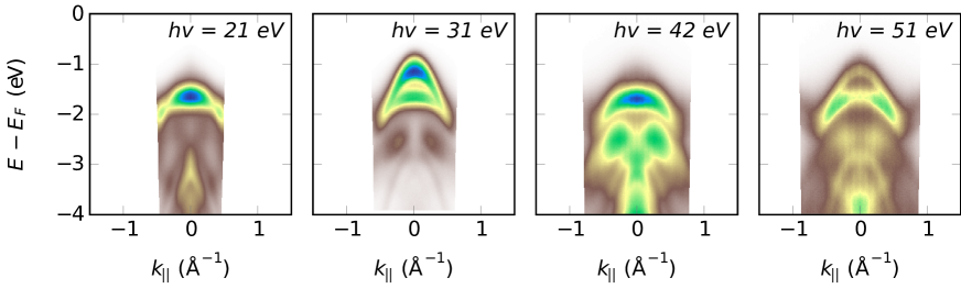
Ever since the discovery of graphene 1, 2, research on two-dimensional (2D) materials is ongoing a tremendous effort. Along with this trend, transition metal dichalcogenides (TMD) are extremely promising for possible technological applications. Their general formula is MX2, where M is a transition element and X is a chalcogene. Those two elements form a MX2 basic layer, where M atoms are sandwiched between two covalently-bonded planes of chalcogenes. The three-dimensional (3D)-solid is obtained by stacking these X-M-X sheets, only weakly bonded by van der Waals interactions 3, conferring to TMD a very pronounced 2D-character. Nowadays, research pushes towards increasingly elaborated structures taking advantage of the 2D nature of these materials: twisted TMD layers 4, hybrid TMD structures (e.g., MoSe2/WSe2, WS2/WSe2) 5, 6, 7 or alloyed TMD systems 8. In the ideal case, these structures are studied by the means of Angle-Resolved PhotoEmission Spectroscopy (ARPES), a technique which allows for direct measurement of the band structure. Its surface sensitivity makes it particularly well-suited to probe 2D-compounds. For bulk TMD-crystals, despite the expected strong 2D-nature of these materials, a significant band dispersion can be observed perpendicular to the MX2-sheets 9, 10, 11. As a matter of fact, both the M- and the X- orbitals (the -axis being perpendicular to the MX2-sheets) point out from the MX2-planes and can hybridize to give rise to this perpendicular dispersion. It can be successfully modeled either using Density Functional Theory (DFT) 10 or a tight-binding approach 11. Nevertheless, DFT-band structure calculations are often made assuming the 2D character of TMD and obtain results on a mesh with only one point. For instance, from calculations presented in reference 12, one could hastily conclude that, at low thicknesses, each new layer in the stacking generates an additional band at . Figure 1 shows dispersions measured on a 2-layer WSe2 sample in directions parallel to for various photon energies, i.e. various position along the direction. We do observe the expected two bands at 31 and 51 eV-photon energies, but not at 21 and 42 eV. That means that even for ultimately thin samples, -effects can be expected, which is more surprising. Previous work on single and bi-layer MoS2 already hinted at those conclusions without proposing a complete explanation 13. These primary observations urge towards a better understanding of the -dependency even for thin samples.
We propose here to study the transition from the 2D-electronic structure of an ultimately thin TMD to a 3D-bulk crystal. We focused on WSe2, whose electronic structure has already been extensively scrutinized 10, 11, 12. The perpendicular dispersion of the band structure is measured by ARPES for sample thicknesses of 2, 3 and N (=6–7) layers. The 2- and N-layer samples were grown by molecular beam epitaxy (MBE) on graphene/SiC (Gr-SiC). To complete the experiment, a 3-layer sample of WSe2 was grown on Mica and then wet-transferred onto a Gr-SiC substrate 14, 15. More details about the samples are given in the Supporting Information.
The ARPES measurements were performed at room temperature on the CASSIOPEE beamline of the SOLEIL synchrotron radiation facility. The samples were first aligned with the -K direction of WSe2 reciprocal lattice along the slit of the analyzer. We call the component of the wave vector parallel to this direction. A (, ) image can then be measured at once thanks to the 2D-detector of the electron analyzer. Here, is the electron binding energy and is measured with respect to the Fermi level . was changed by scanning the photon energy from 20 to 90 eV (and 1 eV-step), which amounts to span a -range from roughly 2.5 to 5 Å-1. Details on the experimental geometry, on the measurement strategy and on the determination of are given in the Supporting Information.
Figure 2 shows a series of ARPES-images recorded on the N-layer sample showing the dispersion along for chosen photons energies between 20 and 90 eV. It clearly evidences large variations of the band structure along (see Figure 3(a)). The vertical black line is at =0.
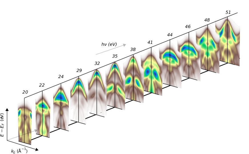
To have a clear view of the -dispersion along , we plot this cut at =0 as a function of the perpendicular component of the wave vector on Figure 3 for the different samples (same data as a function of the photon energy are available in the Supporting Information). Figures 3(b-d) show the raw data for 2, 3 and N-layers samples. For the 2-layer sample, the two bands which are the closest to the Fermi level clearly have a discontinuous -dispersion. It consists in line segments corresponding to -values where these bands appear at =0 in the dispersion. Hence, the top band is visible only for between 3.1 and 3.5 Å-1 (photon energies between 23 and 40 eV); it then disappears to show up again between 4 and 4.6 Å-1 (50 and 70 eV). It has a low intensity from 4.5 to 5 Å-1 (70 to 80 eV) and becomes bright again from 5 Å-1 onwards (85 to 90 eV). It therefore appears and disappears when varying the photon energy, confirming the first observations made on Figure 1. Near, e.g., = 3 or 3.7 Å-1 (20 eV and 43 eV) applying the rule 1 layer = one band at , the sample is indistinguishable from a monolayer system with only one visible band at . Let us note that this is the case around 21 eV, the photon energy produced by He-lamps. The same phenomenon is observable on the 3-layer sample with instead three bands appearing and disappearing. We note that the binding energies are slightly shifted in the 3-layer sample with respect to the 2-layer sample. This derives from the different thicknesses of the Gr-SiC substrate which induce differentiated charge transfers 16. The reader can get more details in the Supporting Information. Nevertheless, the bright segments are shorter in photon energy and more numerous for each band. It starts to draw the clear band oscillations that we clearly see in the N-layer case, where the observed dispersion compares well with previously measured data on bulk-WSe2 10, 11. The same observations can be made on the second derivative images (Figure 3(e-g)).
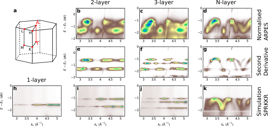
At these very small thicknesses, the electronic states considered here can certainly be seen as 2D-electronic systems, confined within the few atomic layers forming the WSe2-layer. They can then be described as quantum well states whose behaviour in ARPES has been extensively described. The pioneering work of Louie et al. 17 was the first to evidence intensity variations of the Cu(111) Schockley surface state when varying the photon energy, with maxima for -final states corresponding to the -point of the 3D Brillouin zone. Intensity resonances of surface states using photon energies matching vertical transitions at high symmetry points of the 3D Brillouin zones was later confirmed by, e.g., studies on the Al(001) 18 or Cu-vicinal surfaces 19. This is precisely what we observe here, although with some complications coming from the WSe2 crystallographic structure. Taking a -parameter of 12.96 Å 20, one obtains a distance of 0.2424 Å-1. At low thicknesses (2 and 3-layer samples), the maxima observed in our data (around 3.15, 4.12 and 5.1 Å-1) correspond to the positions of the , and -points of the reciprocal space. These maxima are observable on all the samples. The periodicity appears therefore as doubled in the reciprocal space, as compared to what is expected. This has been explained by Finteis et al. 9, following the works of Pescia et al. 21. WSe2 has a hexagonal structure whose primitive cell contains two WSe2-layers (2H-WSe2). It belongs to the -space group which is nonsymmorphic, i.e., it includes a screw axis which is located in the center of the unit cell along the -axis. Group theory implies selection rules for photoemission from the Bloch states on the line of the Brillouin zone that are restricted to the subgroups of and symmetry, respectively, which together with the even parity required for coupling to a free-electron final state, results to allowed optical transition from a given initial state every other Brillouin zone 9.
Our results look very much alike what was obtained on graphene by Ohta et al. 22. On a single layer sample, they showed that the -orbital (forming the famous Dirac cone at the -point of the reciprocal space) is confined in the crystal plane and show no -dispersion. As the number of graphene layers increases, the number of -orbital increases because of interlayer interactions and more and more discrete states appear, gradually converging towards the final 3D-dispersion 22. This is clearly the model system to which our data on WSe2 should be compared. An apparent doubling of the reciprocal space periodicity is also observed, since graphite structure also belongs to a nonsymmorphic space group 21. The interpretation of these results was nicely revisited by Strocov in 2018 23. In this work, ARPES is first interpreted in a Fourier-transform formalism and quantum confined 2D-states are introduced as standing waves multiplied by an envelope function quickly decreasing away from the surface. This lucid model not only confirms that intensity maxima should appear in ARPES at high symmetry points along , but also predicts that these maxima spread over a -range inversely proportional to the -spatial extension of the 2D-state 23. In other words, the "dots" observed at fixed binding energies should gradually shorten as the -delocalization increases. This is what is observed on graphene 22 as well as in our results. Finally, let us note that this intensity behaviour is also well-reproduced by tight-binding calculations performed on a one-dimensional atomic chain of increasing length 24. In the following, we’ll show that different theoretical models can account for this behaviour, including fine details.
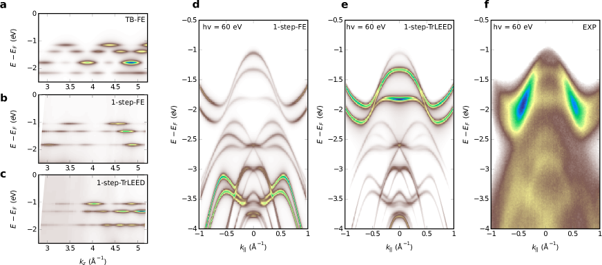
To understand better its physics, we propose to study the system at different levels of approximation using first a tight-binding initial state and free electron (FE) final state (TB-FE model). We then increase the complexity by describing the photoemission process within the one-step model of photoemission 25 as implemented in the SPRKKR package 26 using a free electron final state (1-step-FE model). The last step is the calculation using the one-step model and a time-reversed LEED (TrLEED) final state (1-step-TrLEED model). This last result is presented in Figure 3(h-k) for free-standing 1, 2, 3 and an infinite number of WSe2 layers. They are in excellent agreement with the measured data, reproducing the discontinuous patterns and converging to a bulk-like dispersion.
The tight-binding model 27 is inspired from the derivation made in references 11 and 28. We aim at a minimal model valid at along the direction. For more complete derivations, the reader can refer to references 29, 30, 31, 32, 28. More details about our tight-binding model and the calculation of the photoemission current can be found in the Supporting Information. Figure 4 shows the results of the three types of calculation on the trilayer system. In Figure 4(a), we see that the simple tight-binding model already captures the essential characteristics of the system with discrete energy states appearing in -ranges in a staggered fashion. It underestimates the total amplitude of the dispersion (difference between the lowest level and highest energy level) of 0.2 eV (See Supporting Information for a quantitative comparison of these energy differences at and ). The intensities are only indicative and the model does not resolve the complex symmetry effects due to the screw-axis 9. For this reason, we only show the contribution of the phase corresponding to the dominant photoemission intensity in experiments (, being the interlayer distance, see Supporting Information). Figure 4(b) shows the results for the 1-step-FE model. They are strikingly similar to those of the TB-FE model. They nevertheless show a better agreement with experimental data: the values of the energy levels are more precisely calculated (with discrepancies smaller than 20 meV) and the photoemitted intensity displays additional modulation along . The symmetry effects due to the crystal space group are now consistent with the experimental data. The pattern matches especially well with the measurements in the 2.5 to 4 Å-1 -range. Finally, Figure 4(c) shows the outcome of the 1-step-TrLEED model. In essence, the modulation of intensity is a step closer to experimental data. The -patterning matches extremely well the experiment in the 3.5 to 5.5 Å-1 range. On the other hand, we notice a discrepancy with an excess intensity in the 4.5 Å-1 and onwards range for the top band at -1 eV. Comparing ARPES dispersions in Figure 4(d,e), we see that the 1-step-FE model grossly overestimates the spectral weight of lower energy bands comparatively to those at the top of the valence bands. In the 1-step-TrLEED, the distribution of the spectral weight is improved: the top of the valence bands generally has a higher intensity than the lower lying bands in the experimental data (see Figure 4(f)).
To conclude, the ARPES study of MBE-deposited WSe2 films with variable thickness gives an overview of the evolution of the electronic structure of this TMD during its transition from 2D to 3D. The behaviour observed at thicknesses as low as 2 or 3-layer WSe2, with discrete states appearing at constant binding energies over finite -ranges, are coherent with the predicted signature of 2D-states, confined in the plane of the atomically-thin crystal. Their evolution with an increasing number of layers shows a larger and larger delocalisation as interlayer electronic hoppings become possible. A 6-7 layer film already shows an electronic structure comparable to what was measured on bulk crystals. Phenomenological 23 or simplified 24 models, as well as what is usually observed in 2D surface states account well for our observations, highly similar to what was previously measured on graphene layers 22. Here, the results were completely modeled by various methods with increasing complexity, as a bench test for these models: a simple tight-binding model accounts for most of the experimental observations but does not capture the effects of the crystal symmetry on the photoemission signal. An ab initio calculation in the KKR-Green’s function formalism using a free electron final state is more accurate but fails to reproduce the observed relative intensities of the different bands. A similar calculation using a TrLEED final state improves a lot this aspect. These last two calculations are performed on systems with the real geometry, going from 2D to 3D. The electronic properties of TMD, e.g., the nature (indirect or direct) of their band gap, strongly vary with thickness, both in "classical" TMD 33, 34, or in more sophisticated but close compounds 8. It is therefore of prime interest to know how the electronic structure evolves, as described by our results.
I Associated content
Additional experimental details, materials, and methods
II Acknowledgments
R.S. acknowledges the support of the French National Research Agency (ANR) (CORNFLAKE project, ANR-18-CE24-0015-01). This work was supported by the project Quantum materials for applications in sustainable technologies (QM4ST), funded as project No. CZ.02.01.01/00/22008/0004572 by Programme Johannes Amos Commenius, call Excellent Research. This publication was supported by the project TWISTnSHINE, funded as project No. LL2314 by Programme ERC CZ.
References
- Novoselov et al. 2004 Novoselov, K. S.; Geim, A. K.; Morozov, S. V.; Jiang, D.; Zhang, Y.; Dubonos, S. V.; Grigorieva, I. V.; Firsov, A. A. Electric Field Effect in Atomically Thin Carbon Films. Science 2004, 306, 666–669
- Novoselov et al. 2005 Novoselov, K.; Jiang, D.; Schedin, F.; Booth, T.; Khotkevich, V.; Morozov, S.; Geim, A. Two-dimensional atomic crystals. Proceedings of the National Academy of Sciences 2005, 102, 10451–10453
- Dickinson and Pauling 1923 Dickinson, R. G.; Pauling, L. The crystal structure of molybdenite. J. Am. Chem. Soc. 1923, 45, 1466–1471
- Gatti et al. 2023 Gatti, G. et al. Flat Moiré Bands in Twisted Bilayer WS2. Physical Review Letters 2023, 131, 046401
- Yuan et al. 2020 Yuan, L.; Zheng, B.; Kunstmann, J.; Brumme, T.; Kuc, A. B.; Ma, C.; Deng, S.; Blach, D.; Pan, A.; Huang, L. Twist-angle-dependent interlayer exciton diffusion in WS2–WSe2 heterobilayers. Nature Materials 2020, 1–7
- Stansbury et al. 2021 Stansbury, C. H. et al. Visualizing electron localization of WS2/WSe2 moiré superlattices in momentum space. Science Advances 2021, 7, eabf4387
- Khalil et al. 2022 Khalil, L.; Pierucci, D.; Velez-Fort, E.; Avila, J.; Vergnaud, C.; Dudin, P.; Oehler, F.; Chaste, J.; Jamet, M.; Lhuillier, E.; Pala, M.; Ouerghi, A. Hybridization and localized flat band in the WSe2/MoSe2 heterobilayer. Nanotechnology 2022, 34, 045702
- Ernandes et al. 2021 Ernandes, C.; Khalil, L.; Almabrouk, H.; Pierucci, D.; Zheng, B.; Avila, J.; Dudin, P.; Chaste, J.; Oehler, F.; Pala, M.; Bisti, F.; Brulé, T.; Lhuillier, E.; Pan, A.; Ouerghi, A. Indirect to direct band gap crossover in two-dimensional WS2(1-x) Se2x alloys. npj 2D Materials and Applications 2021, 5, 1–7
- Finteis et al. 1997 Finteis, T.; Hengsberger, M.; Straub, T.; Fauth, K.; Claessen, R.; Auer, P.; Steiner, P.; Hüfner, S.; Blaha, P.; Vögt, M.; Lux-Steiner, M.; Bucher, E. Occupied and unoccupied electronic band structure of WSe2. Physical Review B 1997, 55, 10400–10411
- Riley et al. 2014 Riley, J. M. et al. Direct observation of spin-polarized bulk bands in an inversion-symmetric semiconductor. Nature Physics 2014, 10, 835–839
- Kim et al. 2016 Kim, B. S.; Rhim, J.-W.; Kim, B.; Kim, C.; Park, S. R. Determination of the band parameters of bulk 2H-MX2 (M=Mo, W; X=S, Se) by angle-resolved photoemission spectroscopy. Scientific Reports 2016, 6, 36389
- Nguyen et al. 2019 Nguyen, P. V.; Teutsch, N. C.; Wilson, N. P.; Kahn, J.; Xia, X.; Graham, A. J.; Kandyba, V.; Giampietri, A.; Barinov, A.; Constantinescu, G. C.; Yeung, N.; Hine, N. D. M.; Xu, X.; Cobden, D. H.; Wilson, N. R. Visualizing electrostatic gating effects in two-dimensional heterostructures. Nature 2019, 572, 220–223
- Miwa et al. 2015 Miwa, J. A.; Dendzik, M.; Grønborg, S. S.; Bianchi, M.; Lauritsen, J. V.; Hofmann, P.; Ulstrup, S. Van der Waals Epitaxy of Two-Dimensional MoS2–Graphene Heterostructures in Ultrahigh Vacuum. ACS Nano 2015, 9, 6502–6510
- Salazar et al. 2022 Salazar, R. et al. Visualizing Giant Ferroelectric Gating Effects in Large-Scale WSe2/BiFeO3 Heterostructures. Nano Lett. 2022, 22, 9260–9267
- Dau et al. 2019 Dau, M. T.; Vergnaud, C.; Gay, M.; Alvarez, C. J.; Marty, A.; Beigné, C.; Jalabert, D.; Jacquot, J.-F.; Renault, O.; Okuno, H.; Jamet, M. van der Waals epitaxy of Mn-doped MoSe2 on mica. APL Materials 2019, 7, 051111
- Zhang et al. 2021 Zhang, Y.; Xie, X.; Zong, J.; Chen, W.; Yu, F.; Tian, Q.; Meng, Q.; Wang, C.; Zhang, Y. Charge transfer between the epitaxial monolayer WSe2 films and graphene substrates. Applied Physics Letters 2021, 119, 111602
- Louie et al. 1980 Louie, S. G.; Thiry, P.; Pinchaux, R.; Pétroff, Y.; Chandesris, D.; Lecante, J. Periodic Oscillations of the Frequency-Dependent Photoelectric Cross Sections of Surface States: Theory and Experiment. Phys. Rev. Lett. 1980, 44, 549–553
- Hofmann et al. 2002 Hofmann, P.; Søndergaard, C.; Agergaard, S.; Hoffmann, S. V.; Gayone, J. E.; Zampieri, G.; Lizzit, S.; Baraldi, A. Unexpected surface sensitivity at high energies in angle-resolved photoemission. Phys. Rev. B 2002, 66, 245422
- Lobo and Mascaraque 2006 Lobo, J.; Mascaraque, A. Observation of the noble-metal L-gap surface state in Cu(311). Journal of Physics: Condensed Matter 2006, 18, L395
- Schutte et al. 1987 Schutte, W.; De Boer, J.; Jellinek, F. Crystal structures of tungsten disulfide and diselenide. Journal of Solid State Chemistry 1987, 70, 207–209
- Pescia et al. 1985 Pescia, D.; Law, A.; Johnson, M.; Hughes, H. Determination of observable conduction band symmetry in angle-resolved electron spectroscopies: Non-symmorphic space groups. Solid State Communications 1985, 56, 809–812
- Ohta et al. 2007 Ohta, T.; Bostwick, A.; McChesney, J. L.; Seyller, T.; Horn, K.; Rotenberg, E. Interlayer Interaction and Electronic Screening in Multilayer Graphene Investigated with Angle-Resolved Photoemission Spectroscopy. Phys. Rev. Lett. 2007, 98, 206802
- Strocov 2018 Strocov, V. Photoemission response of 2D electron states. Journal of Electron Spectroscopy and Related Phenomena 2018, 229, 100–107
- Moser 2017 Moser, S. An experimentalist’s guide to the matrix element in angle resolved photoemission. Journal of Electron Spectroscopy and Related Phenomena 2017, 214, 29–52
- Braun et al. 2018 Braun, J.; Minár, J.; Ebert, H. Correlation, temperature and disorder: Recent developments in the one-step description of angle-resolved photoemission. Physics Reports 2018, 740, 1–34, Correlation, temperature and disorder: Recent developments in the one-step description of angle-resolved photoemission
- Ebert et al. 2011 Ebert, H.; Ködderitzsch, D.; Minár, J. Calculating condensed matter properties using the KKR-Green’s function method—recent developments and applications. Reports on Progress in Physics 2011, 74, 096501
- 27 Salazar, R. Code available at https://gitlab.com/SLZ_Raph/arpestb, https://gitlab.com/SLZ_Raph/arpestb
- Amorim 2018 Amorim, B. General theoretical description of angle-resolved photoemission spectroscopy of van der Waals structures. Physical Review B 2018, 97, 165414
- Cappelluti et al. 2013 Cappelluti, E.; Roldán, R.; Silva-Guillén, J. A.; Ordejón, P.; Guinea, F. Tight-binding model and direct-gap/indirect-gap transition in single-layer and multilayer MoS2. Physical Review B 2013, 88, 075409
- Roldán et al. 2014 Roldán, R.; López-Sancho, M. P.; Guinea, F.; Cappelluti, E.; Silva-Guillén, J. A.; Ordejón, P. Momentum dependence of spin–orbit interaction effects in single-layer and multi-layer transition metal dichalcogenides. 2D Materials 2014, 1, 034003
- Fang et al. 2015 Fang, S.; Kuate Defo, R.; Shirodkar, S. N.; Lieu, S.; Tritsaris, G. A.; Kaxiras, E. Ab initio tight-binding Hamiltonian for transition metal dichalcogenides. Physical Review B 2015, 92, 205108
- Silva-Guillen et al. 2016 Silva-Guillen, J. A.; San-Jose, P.; Roldan, R. Electronic Band Structure of Transition Metal Dichalcogenides from Ab Initio and Slater–Koster Tight-Binding Model. Applied Sciences 2016, 6, 284
- Mak et al. 2010 Mak, K. F.; Lee, C.; Hone, J.; Shan, J.; Heinz, T. F. Atomically Thin MoS2: A New Direct-Gap Semiconductor. Phys. Rev. Lett. 2010, 105, 136805
- Radisavljevic et al. 2011 Radisavljevic, B.; Radenovic, A.; Brivio, J.; Giacometti, V.; Kis, A. Single-layer MoS2 transistors. Nature Nanotechnology 2011, 6, 147–150