A Hardware-Friendly Shuffling Countermeasure Against Side-Channel Attacks for Kyber
Abstract
CRYSTALS-Kyber (a.k.a. Kyber) has been drafted to be standardized as the only key encapsulation mechanism (KEM) scheme by the national institute of standards and technology (NIST) to withstand attacks by large-scale quantum computers. However, the side-channel attack (SCA) on its implementation is still needed to be well considered for the upcoming migration. In this brief, we propose a secure and efficient hardware implementation for Kyber by incorporating a novel compact shuffling architecture. First of all, we modify the Fisher-Yates shuffle to make it more hardware-friendly. We then design an optimized shuffling architecture for the well-known open-source Kyber hardware implementation to enhance the security of all the potential side-channel leakage points. Finally, we implement the modified Kyber design on FPGA and evaluate its security and performance. The security is verified by conducting the correlation power analysis (CPA) attacks on the hardware. Meanwhile, FPGA place-and-route results show that the proposed design reports only 8.7% degradation on the hardware efficiency compared with the original unprotected version, much better than existing hiding schemes.
Index Terms:
CRYSTALS-Kyber, hardware implementation, shuffling, side-channel attack, countermeasure.I Introduction
With the rapid development of quantum computing, modern cryptography algorithms are facing serious threats [1]. Since 2016, the national institute of standards and technology (NIST) has launched a standardization competition for post-quantum cryptography (PQC) and solicited proposals from around the world [2], aiming to form new PQC standards ahead of the coming quantum era. During the PQC standardization process, the lattice-based cryptography (LBC) becomes the most competitive category, occupying three of all four winners to be standardized after three rounds of evaluation [3]. CRYSTALS-Kyber (Kyber) is the only key encapsulation mechanism (KEM) protocol among them. During the upcoming transition of existing conventional cryptographic algorithms to Kyber, it is essential to evaluate the security against physical attacks, such as the side-channel attack (SCA).
In recent years, researchers have proven that both software and hardware implementations of Kyber have the possibility for side-channel leakage, and have successfully implemented SCAs [4, 5, 6]. On the software side, Bock et al. [4] successfully recovered the key from the polynomial multiplication in Kyber’s decryption procedure, and Sim et al. [5] proved that the disclosure of sensitive variables in Barrett reduction would have exposed the entire key. On the hardware side, Zhao et al. [6] recently pointed out that there are three side-channel leakage points in Kyber’s decryption procedure, and successfully completed SCA on the open-source hardware implementation from [7].
However, defense work for Kyber, especially on hardware platform, is still far from sufficient, where masking and hiding both are usually adopted countermeasures. Zhao et al. [6] and Kamucheka et al. [8] proposed two different hardware masking schemes, both of which introduce significant area overhead. On the other hand, two hiding schemes on hardware platform are provided in [9] and [10]. In [9], Morait et al. used the method of randomized clock and duplication to reduce the energy correlation during the operation of Kyber. In [10], Jati et al. adopted the methodology of adding random delays and address & instruction shuffling to reduce the energy correlation. Nevertheless, these two hiding schemes result in high resource overhead and clock cycle overhead, respectively. In this brief, we try to propose a hiding protection method for Kyber’s hardware implementation by taking the performance and security both into consideration.
This work provides a good tradeoff between security enhancement and hardware efficiency. Specifically, we modify the Fisher-Yates shuffle [11] to make it more hardware-friendly. Based on the algorithm, we propose an optimized shuffling architecture and apply it to the open-source hardware implementation of Kyber from [7]. We shuffle the sub-operation orders of all the potential side-channel leakage points during Kyber’s decryption procedure. The experimental results show that the proposed design can effectively improve the side-channel security, and reports only 8.7% degradation on the hardware efficiency compared with the original unprotected version.
II Preliminaries
II-A Related Work on Shuffling
As an efficient and effective countermeasure, shuffling is widely used in various cryptographic implementations against SCAs. In recent years, numerous works have been conducted on the security research pertaining to shuffling in the software implementations of lattice-based cryptography. In contrast, there are relatively few studies on the use of shuffling on hardware implementations, as evidenced by the limited entries in Table I. In [10], Jati et al. adopted address & instruction shuffling to reduce the energy correlation. In [12], Chen et al. proposed a low-cost shuffling countermeasure against side-channel attacks for NTT-based post-quantum cryptography. The random permutations used in these two schemes are generated outside of the hardware and preloaded into storage in advance. These schemes require lots of storage space to achieve high security. For example, storing permutations of length 64 would require bits of storage space. In [13], Bayrak et al. proposed a shuffling architecture to generate random permutations. However, under the premise of generating the same size of random permutations, the area consumed by their architecture is almost 4x that of the proposed architecture (only the random permutation generator).
II-B Side-Channel Leakage Points in Kyber
The whole Kyber protocol consists of three procedures, which are key generation, encryption, and decryption. In a cryptographic protocol, the operations that involve both the sensitive values and the intermediate values of plaintext/ciphertext are more prone to side-channel leakage [14]. In the Kyber protocol, the decryption procedure contains multiple operations that satisfy this condition. The main operations of Kyber’s decryption procedure are as follows:
| (1) |
The operations in (1) include number theoretic transform (NTT), point-wise multiplication (PWM), inverse number theoretic transform (INTT), subtraction, and compress, where denotes the decrypted message, denotes the unpacked secret key, and denote the unpacked ciphertext. NTT, PWM, and INTT are used to reduce the complexity of polynomial multiplication. In Kyber’s decryption procedure, Compressq is a function that compresses a polynomial coefficient to 0 or 1, where stands for the modulo . According to [6], there are three side-channel leakage points in Kyber’s decryption procedure (hardware) as shown in (2).
| (2) |
The three leakage points lie in PWM, the modular reduction after PWM, and the subtraction after INTT, respectively. In addition, INTT has been successfully attacked in software implementations [15], so we retain the protection of INTT.
III Proposed Shuffling Architecture for Kyber
Fisher-Yates shuffle [11] is one of the most widely used shuffling algorithms. When it is implemented in hardware, two problems need to be solved. One is to continuously input random seeds and the other is to dynamically reduce the range of indexes. In this work, we have elaborately solved these problems. The key ideas of the improved algorithm will be shown in Algorithm 1.
III-A Random Permutation Generator
Random permutation generator (RPG) is a module that generates random permutations from an ordered one. There are five different random permutations to be generated, which are , , , , and . Since there is a correspondence between these permutations, it is only necessary to generate the permutation , and the other permutations can be obtained by extending it.
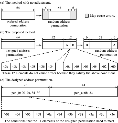
Before introducing the hardware architecture, it is necessary to explain that due to the existence of overlapping addresses, it is necessary to impose restrictions on the first six and last six elements of the randomly generated permutations to avoid address conflicts. The key idea is to specially introduce a fixed intermediate permutation and generate the random one in two stages. The comparison of the shuffling methods without and with adjustment are shown in Fig. 1. As explained above, if we directly use the random address permutation, there may exist errors in the first six or the last six locations as illustrated in Fig. 1(a). To avoid those errors, an intermediate address permutation is specially designed in advance as shown in Fig. 1(c). It is divided into two regions, and , which are defined as:
| (3) |
Note that the first 11 elements from the left of this permutation are designed to satisfy the restrictions shown in Fig. 1(c). Actually, the designed address permutation only needs to restrict those 11 elements and can be in any form. For simplicity, we define it in the above form in this brief.
In the first stage of shuffling, the source of address permutation is and twelve addresses are selected based on the proposed random index permutation, which are placed at the rightmost of a new empty permutation. Those selected locations of are then filled up by the elements of the leftmost of successively. This stage is to protect from errors. In the second stage of shuffling, the rest random addresses are selected from the remaining 52 elements of and . After finishing all the selections, the filled permutation is cyclically shifted to the right 6 times and output as the final random address permutation, as shown in Fig. 1(b).
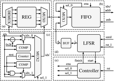
Based on the above analysis, the proposed architecture of RPG is shown in Fig. 2, divided into five parts. Part (a) contains one 64-to-1 MUX named MUX0, one 1-to-64 DEMUX, and one register group named REG with data width of 6 and depth of 64. REG stores the designed address permutation and its updated version. Under the control of , MUX0 outputs an element from REG continuously and DEMUX outputs an element from MUX0 to update the data in REG. Part (b) contains one 3-to-1 MUX and a FIFO with data width of 6 and depth of 64, which is reused to cache the random indexes from the LFSR module and the generated random address permutation to reduce the area consumption. Three control signals are used, i.e., , , and . With the control signals of and , FIFO is worked in the input mode and the cyclic mode, respectively. When FIFO is in the input mode, the data enter from REG or LFSR; and when FIFO is in the cyclic mode, the output is pushed back into the input. Part (c) contains one 3-to-1 MUX named MUX2, two 2-to-1 MUXs, two comparators, one counter, one subtractor, and one AND gate. MUX2 has three inputs, , , and , controlled by . The input random index output from FIFO is adjusted to match the two stages of shuffling, formulated as:
| (4) |
| (5) |
where the value 28 is in the hexadecimal format. The variable rest denotes the number of the remaining elements to be selected minus 1, which is computed by a decrement counter. The output signal is selected from , , and , served as the control signal of MUX0 and DEMUX in (a). Part (d) contains a LFSR (used to continuously generate random numbers) and a buffer. The buffer outputs every six cycles to convert six 1-bit numbers into a 6-bit number. When is equal to 1, LFSR updates the registers by using the input random seed. Part (e) contains a controller made up with several logic circuits. It produce the control signals , , , and based on the input signals and for the other three modules.
To make it more clear, we give an algorithm to illustrate the processing schedule of RPG as shown in Algorithm 1. The generation of random permutations can be divided into four steps: (a) initialization, (b) shuffling_12, (c) shuffling_52, and (d) cyclic shift_6. In the initialization step, LFSR outputs bits to fill up FIFO, and REG is set with the designed address permutation. Note that the 64 registers in REG use to as their serial numbers. In the shuffling_12 step, the 12 random addresses are selected from the 41 () lower-side locations of REG based on the shift-out elements from FIFOout and the equation (4), and cached into FIFOin. Meanwhile, those selected locations of REG are filled up with its elements from the specific locations (corresponding to the dynamic maximum serial number ). After 12 rounds, this step is finished and the shuffling_52 step starts. In this step, the rest 52 addresses in REG are messed up based on the remaining random indexes in FIFO and the equation (5). They are serially chosen and cached into FIFO from the lower-side locations of REG. Assume that when is , the random index is , larger than . When it is computed based on the equation (5), we get the adjusted index equal to . We then use the new index to choose the element in the zeroth register of REG and push it into FIFO from the lower-side. At the same time, the element in the zeroth register is updated by the element in the second register (corresponding to the dynamic maximum serial number ) of REG. When the shuffling_52 step is completed, we start the forth step, i.e., the cyclic shift_6 step. FIFO is shifted six times in the cyclic mode and we get the target random address permutation.
The process of RPG will not increase the consumption of total time of Kyber with this protection since RPG is conducted in parallel with Kyber, costs much less cycles, and has shorter critical path. So we design it in a compact way to simplify the control and save area.
III-B Address Controller
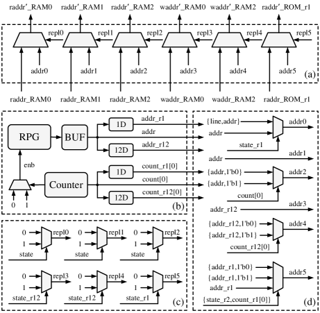
As shown in Fig. 3, the proposed architecture of the address controller (ADDR) is divided into four parts. In part (a), four new read addresses (raddr’_x) and two new write addresses (waddr’_x) are used to replace the read and write addresses of the RAMs and ROM. Six 2-to-1 MUXs are used to determine the data sources of these new addresses. When there is no need for shuffling, the original addresses are directly connected. When shuffling is required, are selected. The generation of the control signals for these MUXs is shown in part (c). In part (b), four shift registers are used to output the delayed random permutations and control signals. The external enable signal of FIFO in RPG is set to 1 every other clock cycle (PWM and subtraction). The generation of is shown in part (d). The permutations and required by , , and can be obtained by concatenating one 0 or 1 after , , and , respectively. The four permutations , , , and required by are obtained by concatenating (equal to ) and into .
IV Results and Comparisons
IV-A Evaluation on SCA Resistance
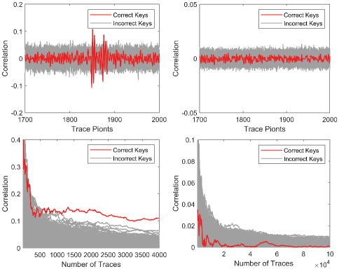
To better assess the level of improvement in side-channel security after applying the protective measures, we conduct correlation power analysis (CPA) attacks (one of the most common SCAs) [16] on PWM for both the unprotected and protected hardware implementations, and the experimental results are shown in Fig. 4. The experimental results indicate that the unprotected Kyber’s hardware implementation can be successfully attacked with a minimum of power traces, while the protected Kyber’s hardware implementation does not show significant correlation even with power traces. It can be concluded that the attack complexity is increased by more than 100x for the attacker. It should be pointed out that the rest leakage points have the similar conclusions as they adopted the same defense countermeasure. We have omitted the experimental results of them here for simplicity.
| Hardware Implementation | Parameter | FPGA Platform | LUTs | FFs | Slices | DSPs | BRAMs | ENS 1 | Cycles () | Frequency (MHz) | ATP 2 (ENS) |
| Xing et al. [7]3 (unprotected) | Kyber512 | Artix-7 | 7,353 | 4,633 | 2,173 | 2 | 3 | 2,973 | 6.7 | 206 | 96.7 |
| Kamucheka et al. [8] | Kyber512 | Virtex-7 | 143,112 | - | 81,746 | 60 | 294 | 146,546 | 126.6 | 100 | 186 |
| Jati et al. [10] | Kyber512 | Artix-7 | 7,151 | 3,730 | 2,260 4 | 2 | 5.5 | 3,560 | 57.2 | 258 | 789.3 |
| This work | Kyber512 | Artix-7 | 8,143 | 5,151 | 2,433 | 2 | 3 | 3,233 | 6.7 | 206 | 105.2 |
| Xing et al. [7]3 (unprotected) | Kyber768 | Artix-7 | 7,353 | 4,633 | 2,173 | 2 | 3 | 2,973 | 10.0 | 206 | 144.3 |
| Moraitis et al. [9] | Kyber768 | Artix-7 | 14,341 | 9,190 | 4,734 4 | 2 | 6 | 6,134 | 10.0 | 206 | 297.8 |
| This work | Kyber768 | Artix-7 | 8,143 | 5,151 | 2,433 | 2 | 3 | 3,233 | 10.0 | 206 | 156.9 |
-
•
1. ENS (equivalent number of slices) = Slices + DSPs 100 + BRAMs 200 [17].
-
•
2. ATP (area-time product) = ENS Time () = ENS Cycles 1/Frequency .
-
•
3. We reevaluate this project using Artix-7 XC7A100T for a fair comparison.
-
•
4. The number of Slices is approximately computed by using LUTs/4 + FFs/8 [17].
IV-B Comparisons on Area and Performance
Table II shows the experiment results and comparison of Kyber’s hardware implementations with different hiding schemes, including the area and time performance. In order to take the DSPs and BRAMs into consideration, we use the equivalent number of slices (ENS) as a new metric for area with the same approximation method used in [17]. For the hardware efficiency, the ATP is computed as ENS Time and listed in the rightmost column of the table. Compared to the unprotected Kyber implementation [7], the proposed protected design only consumes an extra resource of 260 Slices. The numbers of DSPs and BRAMs both are the same. Compared with the unprotected design, the ATP (also area) of the proposed version is increased by only 8.7%.
We also make comparisons with previous protected Kyber hardware implementations. It can be seen that the hiding design proposed in [8] has tremendous area and time consumption, more than three orders of magnitude larger than ours in ATP. The design in [10] has a relatively small area but consumes huge cycles, so its ATP is also much worse than ours. In contrast, the design in [9] has the same clock cycles, but their area is almost twice that of ours.
V Conclusion
In this brief, we have devised an optimized shuffling architecture and integrated it into the Kyber’s hardware implementation to achieve shuffling of all the potential side-channel leakage points during Kyber’s decryption procedure. The experimental results show that the proposed design can effectively improve the side-channel security, and reports only 8.7% degradation on the hardware efficiency compared with the original unprotected version, much better than existing hiding schemes.
References
- [1] P. W. Shor, “Polynomial-Time Algorithms for Prime Factorization and Discrete Logarithms on a Quantum Computer,” SIAM review, vol. 41, no. 2, pp. 303–332, 1999.
- [2] L. Chen, L. Chen, S. Jordan, Y.-K. Liu, D. Moody, R. Peralta, R. A. Perlner, and D. Smith-Tone, Report on Post-Quantum Cryptography. US Department of Commerce, National Institute of Standards and Technology, 2016, vol. 12.
- [3] G. Alagic, D. Apon, D. Cooper, Q. Dang, T. Dang, J. Kelsey, J. Lichtinger, C. Miller, D. Moody, R. Peralta et al., “Status Report on the Third Round of the NIST Post-Quantum Cryptography Standardization Process,” US Department of Commerce, NIST, 2022.
- [4] E. A. Bock, G. Banegas, C. Brzuska, Ł. Chmielewski, K. Puniamurthy, and M. Šorf, “Breaking DPA-protected Kyber via the pair-pointwise multiplication,” Cryptology ePrint Archive, 2023.
- [5] B.-Y. Sim, A. Park, and D.-G. Han, “Chosen-Ciphertext Clustering Attack on CRYSTALS-KYBER Using the Side-Channel Leakage of Barrett Reduction,” IEEE Internet of Things Journal, vol. 9, no. 21, pp. 21 382–21 397, 2022.
- [6] Y. Zhao, S. Pan, H. Ma, Y. Gao, X. Song, J. He, and Y. Jin, “Side Channel Security Oriented Evaluation and Protection on Hardware Implementations of Kyber,” IEEE Transactions on Circuits and Systems I: Regular Papers, 2023.
- [7] Y. Xing and S. Li, “A Compact Hardware implementation of CCA-Secure Key Exchange Mechanism CRYSTALS-KYBER on FPGA,” IACR Transactions on Cryptographic Hardware and Embedded Systems, pp. 328–356, 2021.
- [8] T. Kamucheka, A. Nelson, D. Andrews, and M. Huang, “A Masked Pure-Hardware Implementation of Kyber Cryptographic Algorithm,” in 2022 International Conference on Field-Programmable Technology (ICFPT). IEEE, 2022, pp. 1–1.
- [9] M. Moraitis, Y. Ji, M. Brisfors, E. Dubrova, N. Lindskog et al., “Securing CRYSTALS-Kyber in FPGA Using Duplication and Clock Randomization,” IEEE Design & Test, 2023.
- [10] A. Jati, N. Gupta, A. Chattopadhyay, and S. K. Sanadhya, “A Configurable CRYSTALS-Kyber Hardware Implementation with Side-Channel Potection,” ACM Transactions on Embedded Computing Systems, vol. 23, no. 2, pp. 1–25, 2024.
- [11] R. A. Fisher, “Statistical methods for research workers,” in Breakthroughs in statistics: Methodology and distribution. Springer, 1970, pp. 66–70.
- [12] Z. Chen, Y. Ma, and J. Jing, “Low-cost Shuffling Countermeasures Against Side-Channel Attacks for NTT-Based Post-Quantum Cryptography,” IEEE Transactions on Computer-Aided Design of Integrated Circuits and Systems, vol. 42, no. 1, pp. 322–326, 2022.
- [13] A. G. Bayrak, N. Velickovic, P. Ienne, and W. Burleson, “An Architecture-Independent Instruction Shuffler to Protect Against Side-Channel Attacks,” ACM Transactions on Architecture and Code Optimization (TACO), vol. 8, no. 4, pp. 1–19, 2012.
- [14] M. Azouaoui, O. Bronchain, C. Hoffmann, Y. Kuzovkova, T. Schneider, and F.-X. Standaert, “Systematic Study of Decryption and Re-encryption Leakage: The Case of Kyber,” in International Workshop on Constructive Side-Channel Analysis and Secure Design. Springer, 2022, pp. 236–256.
- [15] M. Hamburg, J. Hermelink, R. Primas, S. Samardjiska, T. Schamberger, S. Streit, E. Strieder, and C. van Vredendaal, “Chosen Ciphertext k-Trace Attacks on Masked CCA2 Secure Kyber,” IACR Transactions on Cryptographic Hardware and Embedded Systems, pp. 88–113, 2021.
- [16] P. Kocher, J. Jaffe, and B. Jun, “Differential Power Analysis,” in Advances in Cryptology—CRYPTO’99: 19th Annual International Cryptology Conference Santa Barbara, California, USA, August 15–19, 1999 Proceedings 19. Springer, 1999, pp. 388–397.
- [17] M. Li, J. Tian, X. Hu, and Z. Wang, “Reconfigurable and High-Efficiency Polynomial Multiplication Accelerator for CRYSTALS-Kyber,” IEEE Transactions on Computer-Aided Design of Integrated Circuits and Systems, 2022.