Oxygen vacancies kinetics in TaO2-h/Ta2O5-x memristive interfaces
Abstract
Oxygen vacancies (OV) are pervasive in metal oxides and play a pivotal role in the switching behaviour of oxide-based memristive devices. In this work we address, through a combination of experiments and theoretical simulations, OV dynamics in Pt/TaO2-h/Ta2O5-x/TaO2-y/Pt devices. In particular, we focus on the RESET transition (from low to high resistance), induced by the application of electrical pulse(s), by choosing different initial OV profiles and studying their kinetics during the mentioned process. We demonstrate that by selecting specific OV profiles it is possible to tune the characteristic time-scale of the RESET. Finally, we show that the implementation of gradual RESETs, induced by applying many (small) successive pulses, allows estimating the activation energies involved in the OV electromigration process. Our results help paving the way for OV engineering aiming at optimizing key memristive figures such as switching speed or power consumption, which are highly relevant for neuromorphic or in-memory computing implementations.
Recent advances in big data manipulation and machine learning demand for low-power in-memory computing operations. Despite substantial progress in software and processing algorithms centered on artificial neural networks [1, 2, 3], the evolution of hardware architectures aiming to avoid the Von Neumann bottleneck continues to encounter substantial challenges. In this scenario, electronic hardware that could mimic the structure and information processing mechanisms of biological systems is emerging as a promising alternative [4, 5, 2]. In particular memristors are playing a essential role [6, 7], contributing to the realization of artificial synapses and in-memory processing and aiming to eliminate the physical separation between memory and processing units characteristic of the usual Von Neumann architectures [8, 9, 10, 11, 12, 13]. Memristors are metal/insulator/metal capacitor-like structures that exhibit the resistive-switching (RS) phenomena, i.e. the reversible change of the electrical resistance upon the application of a electrical stress [14, 15, 16, 17, 18, 19].
In Non-Volatile RS (NVRS) the resistive states persist in time after the electrical stimulus is turned off. Hysteresis current–voltage switching loops are a fingerprint of this behavior. On the other hand, in Volatile RS (VRS) the attained resistive states relax once the electrical stimulus is turned off [20, 13]. Thus, several synaptic and neuron functionalities can be electrically emulated based on the lifespan of the resistance states. In the past years, extensive demonstrations of RS in oxides were realized, mostly on binary oxides such TiO2, HfO2, and Ta2O5 [21, 22, 7, 23]. In particular TayOx based devices stand out among others, exhibiting exceptional figures as ON-OFF ratios up to , retention times above 10 years and endurances of up to cycles [21, 24]. RS has been reported as bipolar and its origin related to the formation and retraction/rupture of nanoscale conducting oxygen vacancies (OV) filaments upon polarity reversal of the applied stimulus, ruling the SET (high to low resistance) and RESET (low to high resistance) transitions respectively [25, 26, 27, 28, 29].
The development of neuromorphic devices based on memristors requires a comprehensive knowledge of the mechanisms ruling the RS. Understanding the role of OV and their dynamics is crucial for extensive optimization (improve the switching speed, minimize the energy consumption, enlarge the endurance) and design of oxide-based memories for neuromorphic applications. Numerous reports show that OV, present as extrinsic or intrinsic defects, play a central role in the RS mechanism [16, 25, 30]. In particular the RESET process in TaOx cross-bar arrays was recently analyzed employing time-resolved pulsed experiments and attributed to the OV motion governed by drift and diffusion processes [31]. Despite the obtention of qualitative knowledge, it remains unclear in which way specific OV profiles and their kinetics affect the RS properties of the devices under electrical bias. In addition, the intricate dynamics involved in OV transport remains incompletely elucidated. Thus, obtaining evidence pertaining to the motion of OV proves challenging and usually involve complex in-operando experiments [32, 33, 34]. In order to pave the way along this central issue, in this work we investigate- using a much simpler experimental approach- the transient electrical response in a Pt/TaO2-h/Ta2O5-x/TaO2-y/Pt device during the RESET process.
Assisted by the Voltage-Enhanced Oxygen Vacancy model (VEOV) [35, 36, 37, 38], we identify the specific OV profile at the origin of the RESET transition and we determine its time evolution, providing an unique insight into OV dynamics along this process. In addition, through the study of successive partial RESETs, we were able to estimate the activation energy for OV migration, which is a key issue for controlling the RS effect and designing efficient operation electrical protocols.
.1 EXPERIMENTAL SET UP
A bilayer Ta-oxide thin film was deposited on commercially platinized silicon using Pulsed Laser Deposition (PLD) -the laser fluence was fixed at 1.5 J cm-2- from a Ta2O5 ceramic target at room temperature. The deposition was made in 2-steps,using oxygen pressures of 0.01 and 0.1 mbar, respectively. We obtained two layers, a more reduced with a thickness of 35 nm and a more oxidized with a 15 nm thickness, as shown in the sketch of Fig. 1(a). It is usually considered that more reduced layers behave as OV source/sink that favors the reduction/oxidation of more oxidized ones, driving the memristive effect [39].
Top Pt electrode was made by sputtering and micro-structured using optical lithography [37]. On the other hand, the Pt of the substrate acts as the bottom electrode, which was grounded. The electrical stimulus (voltage) was applied to the top Pt electrode.
The pristine device starts in a low resistance state of 100 . By applying a negative stimulus of - 3V during 1 ms, an intermediate resistance state of the order of k was attained, awakening the memristive response. The electroformed device results in the stack Pt/TaO2-h/Ta2O5-x/TaO2-y/Pt [37], as sketched in Fig.1 (a). The active zone for RS comprises the more oxidized layer, Ta2O5-x, sandwiched between the two reduced layers, defining a quasi-symmetric configuration with two active memristive interfaces: the top interface (TI) TaO2-h/Ta2O5-x and the bottom interface (BI) Ta2O5-x/TaO2-y, respectively. On the other hand Pt/TaO2-h(y) is an ohmic interface playing a passive role in the RS. The memristive behavior of the device was studied in detailed in Ref.37 and can be understood in terms of OV electromigration between the central zone, Ta2O5-x, and the interfacial regions under the applied stimulus.
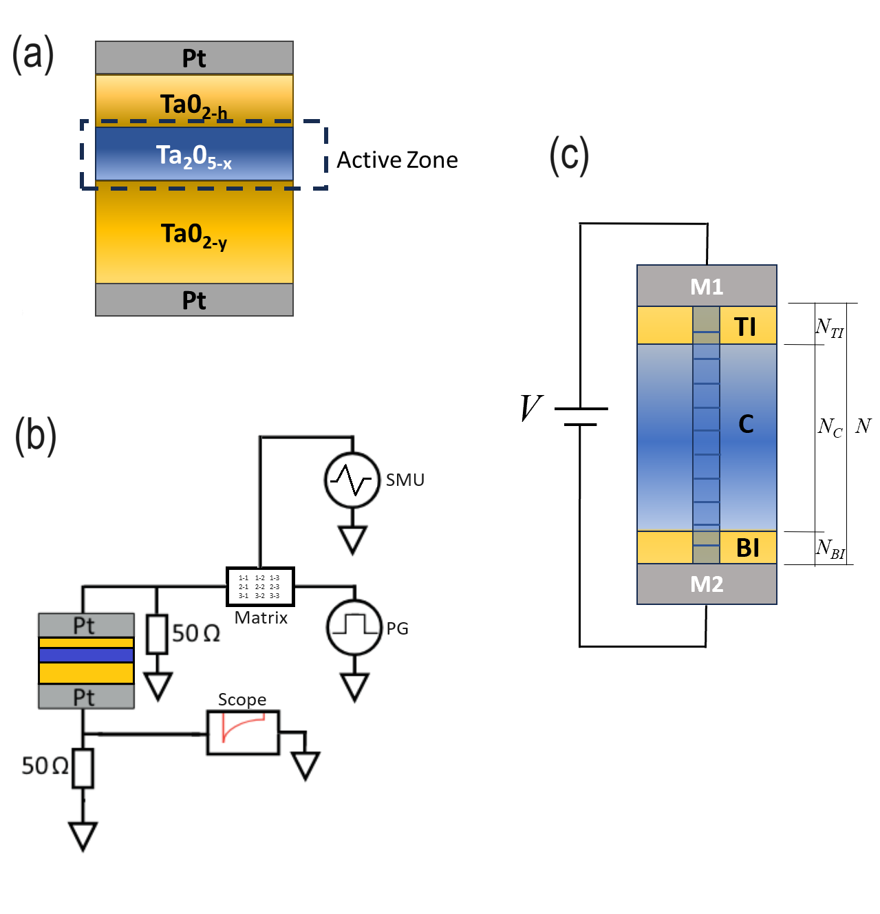
The electrical characterization was performed in two steps. Firstly, using a Keithley 2612 source-meter, we applied the RS protocol (described below in Sec..2) to check the correct RS behavior and tune the desired resistive state of the sample. Then, with an Agilent 81110A pulse generator, a single RESET pulse is applied. A homemade matrix allowed to select the needed instrument in each case. The RESET current response was measured using a shunt connected to a Tektronix TDS5032B Oscilloscope. The experimental setup is shown in Fig.1 (b).
.2 RESULTS
The RS protocol consists of a pulsed ramp that alternates between write pulses, which changes the resistance state of the device, and read pulses that capture their remanent resistance states (see inset of Fig.2 (a)). From these pulses, we obtain respectively, the dynamic I-V curves (not shown) and the so-called Hysteresis Switching Loop (HSL) [35] which displays the remanent resistance as a function of the applied (write) voltage. Depending on the polarity and the symmetry of the voltage protocol, defined by the maximum and minimun intensities (0) and (0), different HSLs with shapes and chiralities -reflecting the activation of one memristive interface, the other or both- can be obtained [37]. For the present device, the HSLs presents a squared-like shape with a clockwise (CW) chirality for , and a counter-clockwise (CCW) chirality for the inverted voltage excursion i.e . In addition, when the voltage excursions are enlarged and symmetrized to , the HSL displays a table with legs (TWL) -like shape [37]. The squared HSLs correspond to a single active interface while the TWL corresponds to two (complementary) active interfaces; that is, when one switches from low to high resistance the other one does it inversely [35]. Therefore, each memristive interface can be selectively activated or deactivated according to the polarity and intensity of the applied stimuli [37, 38].
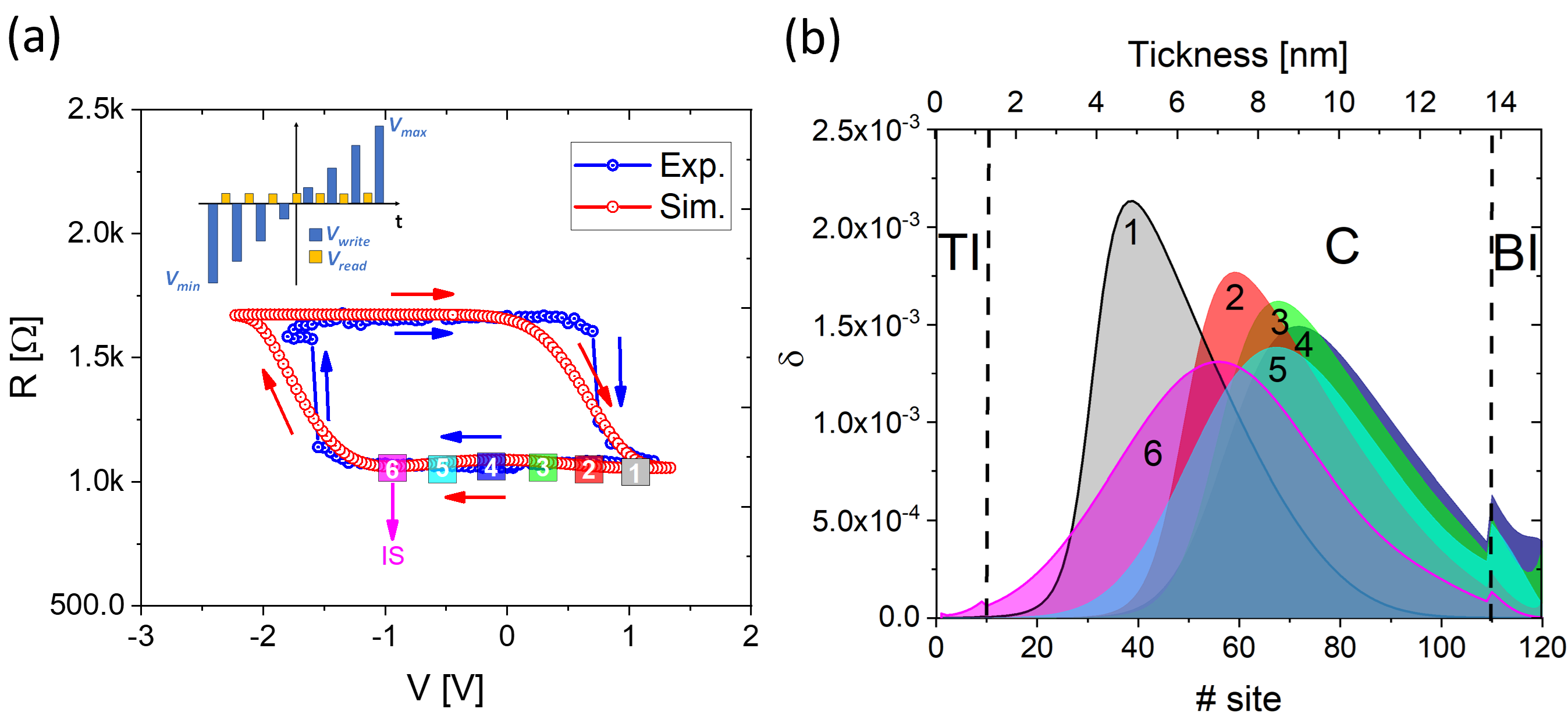
Starting with a post-forming device, we prepared the device in a low resistance state by following the CW HSL, using a non-symmetrical protocol with V and V. The sample was initially cycled several times to ensure stability and repeatability of the CW HSL, displayed in Fig.2 (a) (blue dots), with well-defined LRS (1.05 k), HRS (1.65 k) and SET and RESET voltages, respectively. Notice that the LRS remains almost flat for voltages in the range [1.2 V, -1.2 V], reflecting the time-stability (non-volatility) of the resistance states. We start by analysing the RESET process under the application of single electrical pulses of different intensities. To this end, the device was prepared in the low-resistance state (LRS) just before reaching the RESET threshold. In particular, we chose as the initial state (IS) the resistance 1.05 k , labelled (magenta square) in the CW HSL of Fig.2 (a).
Figure 3(a) shows, in continuous lines, the evolution of the resistance with time during the RESET process for three different voltages applied during 100 s, starting from the chosen IS. A higher voltage induces a complete RESET attaining the HRS in a shorter time, as expected. For -2.8 V, it takes 30s to complete the RESET process, while for -2.6 V it takes 100s. This response is consistent with the fact that for negative voltages, OV -as positive defects- move from the central region towards the TI (TaO2-h/TaO5-x), which is active throughout the entire (RESET) process. Thus, for higher applied voltages, OV (electro) migration is enhanced and therefore the RESET takes place in shorter time scales. In addition, the non-linearity of the resistance as a function of time during the RESET increases with the intensity of the voltage - a characteristic of activated processes previously reported [40, 41]-.
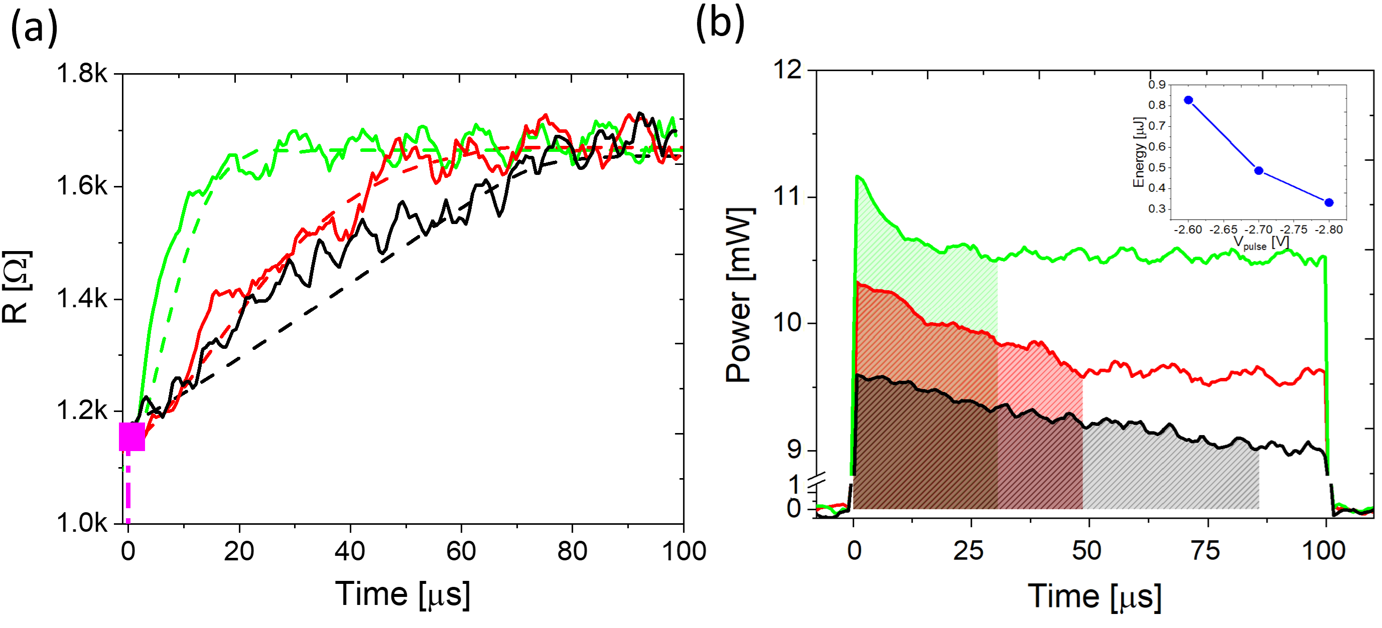
It is interesting to estimate and compare the energy consumption involved in the RESET processes. To this end, we followed Refs. 42, 37 and compute in Fig.3(b) the power consumption as , where values correspond to the measured resistances displayed in Fig.3(a). In addition, the inset shows the energy (computed as the shaded area under each of the curves when the power variation is below 5) for the three voltage values. It is noteworthy that the energy involved in the RESET process is lower for higher pulses intensities, even though the power consumption is larger. This is a clear evidence of the non linear dependence of the RESET process with the applied voltage, in agreement with the voltage-time dilemma typically present in RS devices [41] .
To model the experimental response we used the 1d Voltage-enhanced Oxygen Vacancies Oxygen (VEOV) migration model [35, 36, 37, 38] that describes the resistive change in oxide based memristors as a result of the migration of the ubiquitous OV under the application of external electrical stimuli.
The VEOV model considers a 1d chain of N nanodomains which can contain a specific total amount of OV. Each domain defines a site in the chain and has an associated resistivity, which depends locally on the OV content. In binary oxides of transition metals, OV act as n-type dopants supplying free electrons to the conduction band and thereby reducing the electrical resistance. In agreement with this, we define the resistivity of each nanodomain as , being the OV concentration at site (i.e. the ratio between the number of OV at site i over the total amount of OV), is a parameter that depends on the zone where the domain is located (i.e. interface or not-interface zones) and is the resistivity of the oxide in the absence of OV [36]. The total resistance of the device is computed as with c being a geometric pre-factor.
For the present case, and due to the aforementioned interfaces, the chain of nanodomains is divided into three regions: TI and BI (associated with the interfaces) which allocate and sites respectively and region C that represents the bulk zone of the device, as depicted in Fig. 1 (c). For a given external stimulus , at each simulation step the OV concentrations are updated with the transfer rate , from site to site , which is proportional to the OV concentration at site and to the availability of the neighbouring sites . The exponential Arrhenius factor contains- given in units of thermal energy - the activation energy for OV diffusion (that could vary along different regions of the chain) and the local potential drop at each site, , due to the external electrical stimulus. With the new OV’s concentrations, the local resistivities and the total resistance are therefore updated. In order to emulate the electrical response of the device during the RESET we established an equivalence between experimental and numerical parameters (see the Suppl. Mat.).
Following the described procedure we computed the remanent resistance as a function of and obtained the HSL depicted (in red) in Fig.2 (a), which is in good agreement with the experimental (in blue) one. In particular, the simulated HRS and LRS are almost indistinguishable from the experimental values.
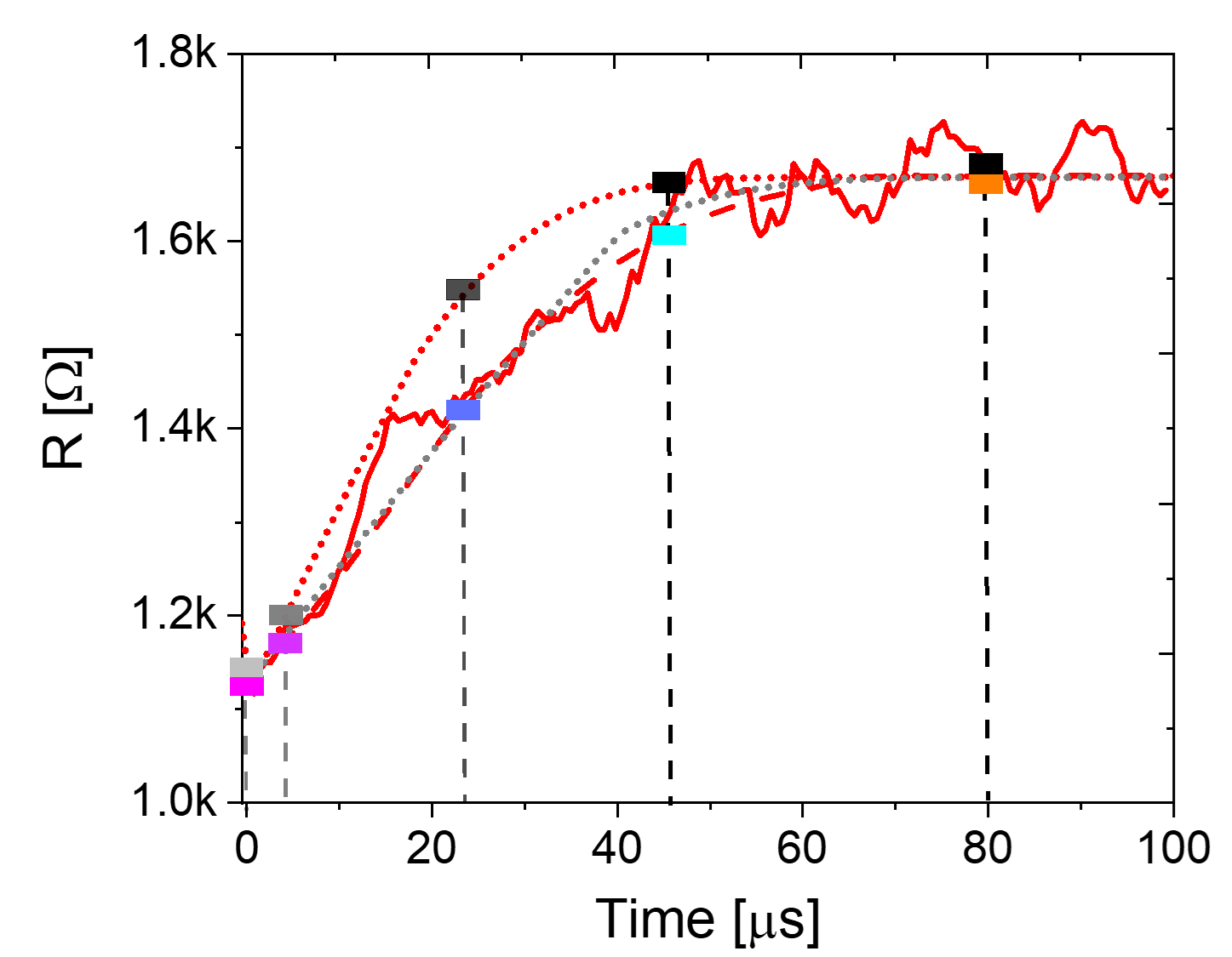
A key outcome of the VEOV model are the OV profiles associated to the different resistance states [35, 36, 43, 37, 38]. In particular, each of the states labelled from 1 to 6 in Fig.2(a) has associated the OV profiles displayed in Fig.2(b)-labelled with the same numbers as their resistance counterparts. These profiles could be taken as different initial condition to simulate the RESET process by applying a single electrical pulse. However, as we already mentioned, the experiment was performed starting from the IS which, according to the VEOV model, has associated the OV profile 6 in Fig. 2 (b). The simulated RESET process for this IS is displayed in Fig.3 (a) in dashed lines for the three voltages considered. The agreement with the experimental results is quite good and, in particular, the simulations follow nicely the experimental curves for = -2.7 and -2.8 V. We notice that IS profile 6 is Gaussian-like, providing a clue about the actual OV distribution prior to the RESET transition.
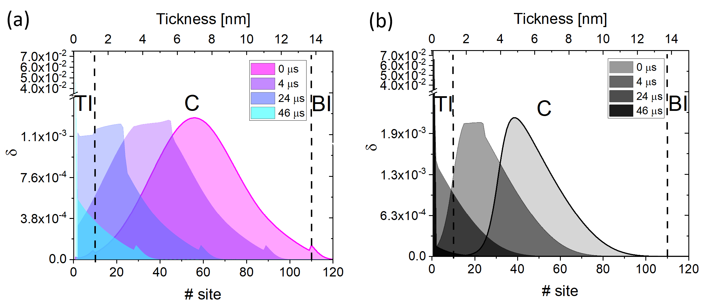
Figure 4 (a) shows the OV profiles for the IS (at time 0 ) and for times 4, 24, and 46 , selected along the simulated RESET displayed in Fig.5 (red-dashed line), for -2.7 V. Notice that, as time evolves, OV profiles move to the TI and accumulate there, acquiring a shape that strongly departs from the initial Gaussian-like shape, as expected for a non diffusive dynamics driven by an external field. In particular, the OV profile for 80 (not shown) -once the complete RESET is attained- is extremely sharp and localized along the first few sites.
For the sake of comparison, we plot in Fig. 4 (b) the OV profiles obtained from the simulated RESET for =-2.7 V - displayed in Fig.5 (red-dotted lines)- starting from the low resistance state labelled 1 in Fig.2 (a). Despite the fact that the initial and final resistance values for profiles 1 and 6 are barely distinguishable , their transient dynamics are clearly different. Profile 1 completes the RESET faster than profile 6, as depicted in Fig. 5. For profile 1, the simulated RESET is completed in 46 , while neither the experimental data (red solid red) nor the simulated evolution starting from the IS (red dashed line) -which nicely follows the experimental curve- have attained the RESET for that time. This is a direct consequence of the fact that the initial OV distribution for profile 1 -which is slightly non-Gaussian- has its maximum closer to the TI than the IS profile 6. Therefore, for profile 1 it should be possible, by lowering the external stimulus, to slow OV dynamics in order to have a resistance vs. time evolution that matches the one obtained for the initial IS stimulated with a -2.7V pulse. Indeed, we depict in Fig. 5 (grey-dotted line) the simulated RESET obtained from profile 1 for -2.65V, which follows the experimental RESET curve almost with the same trend as the IS for -2.7V.
Thus, a clever strategy to reduce the RESET time and, additionally, optimize the power consumption, could be to engineer the initial OV profile [44], as barely different OV distributions with quite similar resistance values give rise to experimentally accessible lower RESET times for the same applied stimulus or, alternative, similar RESET curves for lower stimulus.
The VEOV model was recently extended from 1d to 2d (2d-VEOV), as a tool to describe how OV electromigration is affected by the presence of structural or morphological defects, such as dislocations or grain boundaries. For the present analysis, we have not taken into account those defects, as we do not have experimental evidence pointing to any strong influence of such type of morphological defects, neither from the electrical measurements nor the structural characterization perfomed for this sample [37]. However, we analyzed the transient dynamics with the 2d VEOV model in the plane for different initial OV distributions, when an external stimulus is applied along the direction (see Supp. Mat.). Although the OV evolution during the transient process depends on the shape and location of the initial OV distribution, after a characteristic time scale an uniform OV profile is attained along the direction while a Gaussian-like profile is obtained in the direction, for the studied initial conditions. The uniformization in the direction takes place for time scales much shorter than the time needed in the experiment for cycling until the stable HSL depicted in Fig. 2 (a) is obtained. Therefore, under this result, we safely simulate the actual RESET process in terms of many parallel OV 1d channels along the direction, employing the 1d version of the VEOV model, which consumes significantly less computing time.
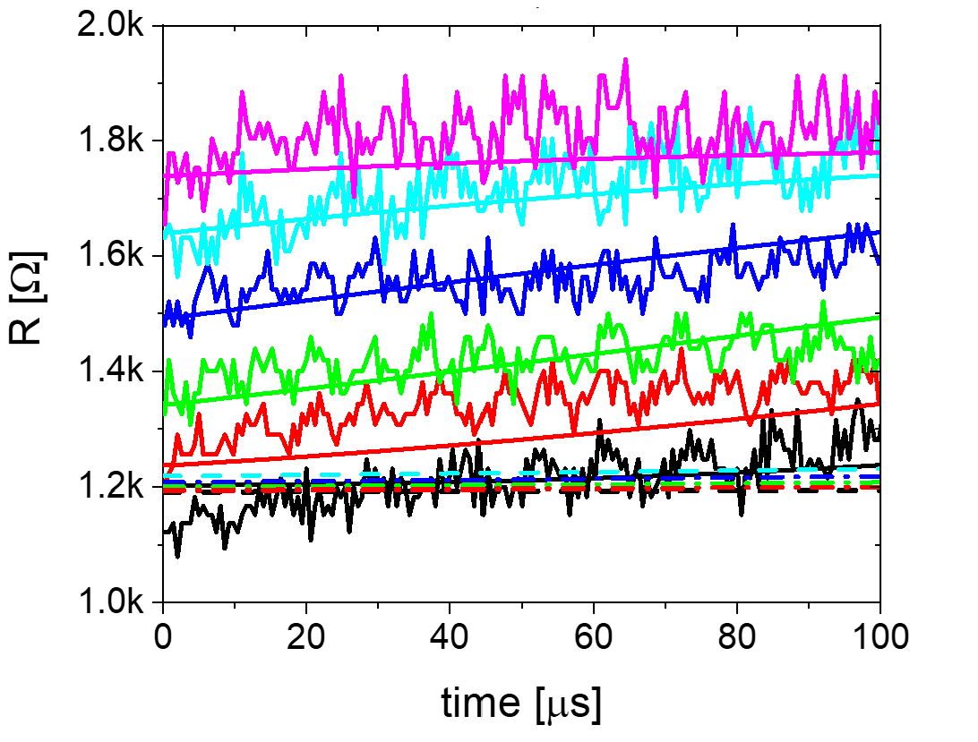
As previously discussed, it is clear that reducing the amplitude of the applied voltage could lead to a situation where a single electrical pulse could not be enough to produce a complete RESET, i.e. the device does not reach its HRS. An interesting avenue to explore is to apply many consecutive pulses of lower intensities [45, 46], each producing a partial RESET. In Fig.6 we show the experimental evolution of the remanent resistance for six successive single pulses of V= -2.4 V with a duration of 100 s applied starting from the IS. Each pulse produces a partial RESET that progressively increases the resistance. In this protocol, the attained resistance for a given pulse is taken as the initial state for the subsequent pulse. Notice that once the complete RESET is achieved (in the present case after six pulses), the HRS resistance remains constant in time -besides the existence of some experimental fluctuations-. The simulated partial RESETs reproduce quite accurately the experimental ones, as shown in Fig.6 with solid lines following the experimental trend. Moreover, when the amplitude of the pulses is reduced to -2.3 V, the initial resistance value remains almost unchanged after the sequence of six pulses ended, as it is shown by the horizontal dashed lines. We stress that this response persists even after increasing the number of applied pulses.
Finally, we show now how the already displayed partial RESET transitions can be used to estimate the OV activation energies. If we aim to reproduce the multiple partial RESETs using number of pulses -each one of 100- given by the experiments, we notice that the VEOV model present two possible control parameters, and , which are added in the argument of the exponential function that defines the Arrhenius factor that controls the OV transfer rate . Lower values (higher values) imply that fewer pulses are needed to reach the HRS, while higher values (lower values) require more pulses to achieve the same HRS. It is noteworthy that the same response could be achieved by adjusting both parameters, provided that the quantity remains unchanged. Additionally, as we have shown, there is an external threshold voltage below which the resistance exhibits no evolution or resistive changes regardless of the number of applied pulses. Above this threshold, the system starts to exhibit resistive changes. With this threshold voltage we can define an effective potential barrier , where for simplicity we assume a linear voltage drop with .
Thus, given a value of , in the simulations we can tune the external voltage in order to determine , and consequently compute . In the present case, we varied the external voltage until for six consecutive pulses the resistive change was below 5 of full RESET. With this criteria we obtained for the example depicted by the dashed lines in Fig. 6. We assume that the experimental threshold voltage, , is equal to numerical one, . Increments of V are fixed by the accuracy of the pulse generator, imposing an uncertainty in .
By increasing the external voltage to , we reproduce the six experimental partial RESETs, depicted by solid lines in Fig.6, and non-trivial characteristics of the observed behavior. In this context, we have consider the difference as the experimental uncertainty.
With these ingredients at hand we can estimate an effective potential barrier for OV electromigration representative of the memristive system under study, by comparing simulations with experimental data. Following this reasoning, for the present case we use -2.3 V () and from the value of employed in the simulations (see Sup. Material) we estimate eeV, in consistency with reported values [47].
I Concluding remarks
We investigated the RESET process and the associated OV dynamics for a Pt/TaO2-h/Ta2O5-x/TaO2-y/Pt memristive device, using a combination of experimental methods and theoretical simulations based on the VEOV model. We focus on the complete RESET process, which involves the transition from LR to the HR state under electrical stress, providing insights into the distribution and kinetics of OVs throughout the device during this process. An interesting outcome of our analysis is that quite similar initial (low) resistance values can have associated different OV profiles the corresponding RESET transitions are completed in different times. Thus, it appears that engineering the OV profiles could be a possible route to change the time scale of this process.
Additionally, by applying several successive pulses inducing gradual RESETs, we were able to estimate the activation energies associated with OV electromigration, resulting in very good agreement with reported values [47]. This further evidences that the VEOV model is powerful enough to extract relevant energy scales and system´s parameter values. In addition, we notice that by using the 2d VEOV model it should be possible to extend the present study to systems including
different types of extended defects. This will allow determining the influence of these defects on the memristive behaviour of oxide-based devices. We notice that this could be the key to obtain physical information about the origin of cycle-to-cycle and/or device-to-device variations, which are usually present in RS devices and are often attributed to the present of (uncontrolled) defects, stabilized during the device fabrication process. [44, 48, 49, 50]. This topic deserves further consideration and we leave it for a future work.
We acknowledge support from ANPCyT (PICT2019-02781, PICT2019-0654, PICT2020A-00415), UNCuyo(06/C026-T1) and EU-H2020-RISE project MELON (Grant No. 872631)
Supplementary Material
See Supplementary Material for additional information on the electrical characterization, system parameters and for the analysis of the OV dynamics employing the 2d VEOV model.
AUTHOR DECLARATIONS
Conflict of Interest
The authors have no conflicts to disclose.
Data availability
The data that support the findings of this study are available from the corresponding author upon reasonable request.
References
- LeCun et al. [2015] Y. LeCun, Y. Bengio, and G. Hinton, Deep learning, nature 521, 436 (2015).
- Zhang et al. [2020] W. Zhang, B. Gao, J. Tang, P. Yao, S. Yu, M.-F. Chang, H.-J. Yoo, H. Qian, and H. Wu, Neuro-inspired computing chips, Nature electronics 3, 371 (2020).
- Ning et al. [2023] H. Ning, Z. Yu, Q. Zhang, H. Wen, B. Gao, Y. Mao, Y. Li, Y. Zhou, Y. Zhou, J. Chen, et al., An in-memory computing architecture based on a duplex two-dimensional material structure for in situ machine learning, Nature nanotechnology 18, 493 (2023).
- Upadhyay et al. [2019] N. K. Upadhyay, H. Jiang, Z. Wang, S. Asapu, Q. Xia, and J. Joshua Yang, Emerging memory devices for neuromorphic computing, Advanced Materials Technologies 4, 1800589 (2019).
- Kendall and Kumar [2020] J. D. Kendall and S. Kumar, The building blocks of a brain-inspired computer, Applied Physics Reviews 7 (2020).
- Valov and Kozicki [2013] I. Valov and M. N. Kozicki, Cation-based resistance change memory, Journal of Physics D: Applied Physics 46, 074005 (2013).
- Kumar et al. [2022] S. Kumar, X. Wang, J. P. Strachan, Y. Yang, and W. D. Lu, Dynamical memristors for higher-complexity neuromorphic computing, Nature Reviews Materials 7, 575 (2022).
- Li et al. [2018] C. Li, D. Belkin, Y. Li, P. Yan, M. Hu, N. Ge, H. Jiang, E. Montgomery, P. Lin, Z. Wang, et al., Efficient and self-adaptive in-situ learning in multilayer memristor neural networks, Nature Communications 9, 2385 (2018).
- Mehonic et al. [2020] A. Mehonic, A. Sebastian, B. Rajendran, O. Simeone, E. Vasilaki, and A. J. Kenyon, Memristors—from in-memory computing, deep learning acceleration, and spiking neural networks to the future of neuromorphic and bio-inspired computing, Advanced Intelligent Systems 2, 2000085 (2020).
- Sebastian et al. [2020] A. Sebastian, M. Le Gallo, R. Khaddam-Aljameh, and E. Eleftheriou, Memory devices and applications for in-memory computing, Nature nanotechnology 15, 529 (2020).
- Yao et al. [2020] P. Yao, H. Wu, B. Gao, J. Tang, Q. Zhang, W. Zhang, J. J. Yang, and H. Qian, Fully hardware-implemented memristor convolutional neural network, Nature 577, 641 (2020).
- Sun et al. [2021] K. Sun, J. Chen, and X. Yan, The future of memristors: Materials engineering and neural networks, Advanced Functional Materials 31, 2006773 (2021), https://onlinelibrary.wiley.com/doi/pdf/10.1002/adfm.202006773 .
- Zhou et al. [2022] G. Zhou, Z. Wang, B. Sun, F. Zhou, L. Sun, H. Zhao, X. Hu, X. Peng, J. Yan, H. Wang, W. Wang, J. Li, B. Yan, D. Kuang, Y. Wang, L. Wang, and S. Duan, Volatile and nonvolatile memristive devices for neuromorphic computing, Advanced Electronic Materials 8, 2101127 (2022), https://onlinelibrary.wiley.com/doi/pdf/10.1002/aelm.202101127 .
- Sawa [2008] A. Sawa, Resistive switching in transition metal oxides, Materials Today 11, 28 (2008).
- Yang et al. [2008] J. Yang, M. Pickett, X. Li, D. Ohlberg, D. Stewart, and R. Williams, A fast, high-endurance and scalable nonvolatile memory device made from asymmetric Ta2O5-x/TaO2-x bilayer structures, Nat. Nanotechnol 3, 429 (2008).
- Waser and Aono [2010] R. Waser and M. Aono, Nanoionics-based resistive switching memories, in Nanoscience And Technology: A Collection of Reviews from Nature Journals (World Scientific, 2010) pp. 158–165.
- Borghetti et al. [2010] J. Borghetti, G. S. Snider, P. J. Kuekes, J. J. Yang, D. R. Stewart, and R. S. Williams, Nature 464, 873 (2010).
- Panda and Tseng [2014] D. Panda and T.-Y. Tseng, Perovskite oxides as resistive switching memories: A review, Ferroelectrics 471, 23 (2014), https://doi.org/10.1080/00150193.2014.922389 .
- Wang et al. [2020] Z. Wang, H. Wu, G. W. Burr, C. S. Hwang, K. L. Wang, Q. Xia, and J. J. Yang, Resistive switching materials for information processing, Nature Reviews Materials 5, 173 (2020).
- Zhuo et al. [2013] V. Y.-Q. Zhuo, Y. Jiang, M. H. Li, E. K. Chua, Z. Zhang, J. S. Pan, R. Zhao, L. P. Shi, T. C. Chong, and J. Robertson, Band alignment between Ta2O5 and metals for resistive random access memory electrodes engineering, Applied Physics Letters 102, 062106 (2013).
- Lee et al. [2011] M.-J. Lee, C. B. Lee, D. Lee, S. R. Lee, M. Chang, J. H. Hur, Y.-B. Kim, C.-J. Kim, D. H. Seo, S. Seo, U.-I. Chung, I.-K. Yoo, and K. Kim, A fast, high-endurance and scalable non-volatile memory device made from asymmetric Ta2O5-x/TaO2-x bilayer structures, Nature Materials 10, 625 (2011).
- Gale [2014] E. Gale, Tio2-based memristors and reram: materials, mechanisms and models (a review), Semiconductor Science and Technology 29, 104004 (2014).
- Yongyue Xiao and Ye [2023] Z. Z. S. K. Y. J. X. W. Yongyue Xiao, Bei Jiang and C. Ye, A review of memristor: material and structure design, device performance, applications and prospects, Science and Technology of Advanced Materials 24, 2162323 (2023), pMID: 36872944, https://doi.org/10.1080/14686996.2022.2162323 .
- Breuer et al. [2016] T. Breuer, L. Nielen, B. Roesgen, R. Waser, V. Rana, and E. Linn, Realization of minimum and maximum gate function in ta2o5-based memristive devices, Scientific reports 6, 23967 (2016).
- Bae et al. [2012] Y. C. Bae, A. R. Lee, J. B. Lee, J. H. Koo, K. C. Kwon, J. G. Park, H. S. Im, and J. P. Hong, Oxygen ion drift-induced complementary resistive switching in homo tiox/tioy/tiox and hetero tiox/tion/tiox triple multilayer frameworks, Advanced functional materials 22, 709 (2012).
- Chen et al. [2015] J.-Y. Chen, C.-W. Huang, C.-H. Chiu, Y.-T. Huang, and W.-W. Wu, Switching kinetic of vcm-based memristor: evolution and positioning of nanofilament, Advanced Materials 27, 5028 (2015).
- Park et al. [2015] T. H. Park, S. J. Song, H. J. Kim, S. G. Kim, S. Chung, B. Y. Kim, K. J. Lee, K. M. Kim, B. J. Choi, and C. S. Hwang, Thickness effect of ultra-thin Ta2O5 resistance switching layer in 28 nm-diameter memory cell, Scientific Reports 5, 15965 (2015).
- Huang et al. [2018] W. Huang, Y.-W. Fang, Y. Yin, B. Tian, W. Zhao, C. Hou, C. Ma, Q. Li, E. Y. Tsymbal, C.-G. Duan, et al., Solid-state synapse based on magnetoelectrically coupled memristor, ACS applied materials & interfaces 10, 5649 (2018).
- Kim et al. [2020] T. Kim, H. Son, I. Kim, J. Kim, S. Lee, J. K. Park, J. Y. Kwak, J. Park, and Y. Jeong, Reversible switching mode change in ta2o5-based resistive switching memory (reram), Scientific Reports 10, 11247 (2020).
- Balatti et al. [2013] S. Balatti, S. Larentis, D. Gilmer, and D. Ielmini, Multiple memory states in resistive switching devices through controlled size and orientation of the conductive filament, Advanced materials 25, 1474 (2013).
- Marchewka et al. [2016] A. Marchewka, B. Roesgen, K. Skaja, H. Du, C.-L. Jia, J. Mayer, V. Rana, R. Waser, and S. Menzel, Resistive switching memory: Nanoionic resistive switching memories: On the physical nature of the dynamic reset process (adv. electron. mater. 1/2016), Advanced Electronic Materials 2 (2016), https://onlinelibrary.wiley.com/doi/pdf/10.1002/aelm.201670006 .
- Herpers et al. [2014] A. Herpers, C. Lenser, C. Park, F. Offi, F. Borgatti, G. Panaccione, S. Menzel, R. Waser, and R. Dittmann, Spectroscopic proof of the correlation between redox-state and charge-carrier transport at the interface of resistively switching Ti/PCMO devices, Advanced Materials 26, 2730 (2014).
- Nukala et al. [2021] P. Nukala, M. Ahmadi, Y. Wei, S. de Graaf, E. Stylianidis, T. Chakrabortty, S. Matzen, H. W. Zandbergen, A. Björling, D. Mannix, D. Carbone, B. Kooi, and B. Noheda, Reversible oxygen migration and phase transitions in hafnia-based ferroelectric devices, Science 372, 630 (2021).
- Jan et al. [2023] A. Jan, T. Rembert, S. Taper, J. Symonowicz, N. Strkalj, T. Moon, Y. S. Lee, H. Bae, H. J. Lee, D.-H. Choe, J. Heo, J. MacManus-Driscoll, B. Monserrat, and G. Di Martino, In operando optical tracking of oxygen vacancy migration and phase change in few nanometers ferroelectric hzo memories, Advanced Functional Materials 33, 2214970 (2023).
- Rozenberg et al. [2010] M. J. Rozenberg, M. J. Sánchez, R. Weht, C. Acha, F. Gomez-Marlasca, and P. Levy, Mechanism for bipolar resistive switching in transition-metal oxides, Phys. Rev. B 81, 115101 (2010).
- Ghenzi et al. [2013] N. Ghenzi, M. J. Sánchez, and P. Levy, A compact model for binary oxides-based memristive interfaces, J. Phys. D: Appl. Phys. 46, 415101 (2013).
- Ferreyra et al. [2020] C. Ferreyra, M. Sánchez, M. Aguirre, C. Acha, S. Bengió, J. Lecourt, U. Lüders, and D. Rubi, Selective activation of memristive interfaces in TaOx-based devices by controlling oxygen vacancies dynamics at the nanoscale, Nanotechnology 31, 155204 (2020).
- Martir et al. [2022] R. L. Martir, M. J. Sánchez, M. Aguirre, W. Quiñonez, C. Ferreyra, C. Acha, J. Lecourt, U. Lüders, and D. Rubi, Oxygen vacancy dynamics in pt/tiox/taoy/pt memristors: exchange with the environment and internal electromigration, Nanotechnology 34, 095202 (2022).
- Lee et al. [2018] M.-J. Lee, G.-S. Park, D. H. Seo, S. M. Kwon, H.-J. Lee, J.-S. Kim, M. Jung, C.-Y. You, H. Lee, H.-G. Kim, S.-B. Pang, S. Seo, H. Hwang, and S. K. Park, Reliable multivalued conductance states in taox memristors through oxygen plasma-assisted electrode deposition with in situ-biased conductance state transmission electron microscopy analysis, ACS Applied Materials & Interfaces 10, 29757 (2018), pMID: 30033726, https://doi.org/10.1021/acsami.8b09046 .
- Schroeder et al. [2010] H. Schroeder, V. V. Zhirnov, R. K. Cavin, and R. Waser, Voltage-time dilemma of pure electronic mechanisms in resistive switching memory cells, Journal of applied physics 107 (2010).
- Menzel et al. [2015] S. Menzel, U. Böttger, M. Wimmer, and M. Salinga, Physics of the switching kinetics in resistive memories, Advanced Functional Materials 25, 6306 (2015), https://onlinelibrary.wiley.com/doi/pdf/10.1002/adfm.201500825 .
- Ferreyra et al. [2019] C. Ferreyra, W. R. Acevedo, R. Gay, D. Rubi, and M. J. Sánchez, Oxygen vacancy dynamics in redox-based interfaces: tailoring the memristive response, Journal of Physics D: Applied Physics 53, 015302 (2019).
- Ghenzi et al. [2014] N. Ghenzi, M. J. Sánchez, D. Rubi, M. J. Rozenberg, C. Urdaniz, M. Weissman, and P. Levy, Tailoring conductive filaments by electroforming polarity in memristive based TiO2 junctions, Applied Physics Letters 104, 183505 (2014).
- Banerjee et al. [2020] W. Banerjee, Q. Liu, and H. Hwang, Engineering of defects in resistive random access memory devices, Journal of Applied Physics 127, 051101 (2020), https://pubs.aip.org/aip/jap/article-pdf/doi/10.1063/1.5136264/19892156/051101_1_1.5136264.pdf .
- Ghenzi et al. [2010] N. Ghenzi, M. Sánchez, F. Gomez-Marlasca, P. Levy, and M. Rozenberg, Hysteresis switching loops in ag-manganite memristive interfaces, Journal of Applied Physics 107, 093719 (2010).
- Ghenzi et al. [2012] N. Ghenzi, M. J. Sánchez, M. J. Rozenberg, P. Stoliar, F. G. Marlasca, D. Rubi, and P. Levy, Optimization of resistive switching performance of metal-manganite oxide interfaces by a multipulse protocol, Journal of Applied Physics 111, 084512 (2012), https://pubs.aip.org/aip/jap/article-pdf/doi/10.1063/1.4705283/14767913/084512_1_online.pdf .
- Hur [2019] J.-H. Hur, The origin of the exceptionally low activation energy of oxygen vacancy in tantalum pentoxide based resistive memory, Scientific Reports 9, 17019 (2019).
- Bischoff et al. [2022] C. Bischoff, J. Leise, E. P.-B. Quesada, E. Perez, C. Wenger, and A. Kloes, Implementation of device-to-device and cycle-to-cycle variability of memristive devices in circuit simulations, Solid-State Electronics 194, 108321 (2022).
- Xu et al. [2023] P. Xu, W. Fa, and S. Chen, Computational study on filament growth dynamics in microstructure-controlled storage media of resistive switching memories, ACS Nano 17, 10511–10520 (2023).
- Park et al. [2024] J. Park, A. Kumar, Y. Zhou, S. Oh, J.-H. Kim, Y. Shi, S. Jain, G. Hota, E. Qiu, A. L. Nagle, I. K. Schuller, C. D. Schuman, G. Cauwenberghs, and D. Kuzum, Multi-level, forming and filament free, bulk switching trilayer rram for neuromorphic computing at the edge, Nat. Comm. 15, 3492 (2024), 10.1038/s41467-024-46682-1 .