Landau Level Single-Electron Pumping
Abstract
We present the first detailed study of the effect of a strong magnetic field on single-electron pumping in a device utilising a finger-gate split-gate configuration. In the quantum Hall regime, we demonstrate electron pumping from Landau levels in the leads, where the measurements exhibit pronounced oscillations in the lengths of the pumping plateaus with the magnetic field, reminiscent of Shubnikov-de Haas oscillations. This similarity indicates that the pumping process is dependent on the density of states of the 2D electron gas over a narrow energy window. Based on these observations, we develop a new theoretical description of the operation of single-electron pumps which for the first time allows for the determination of the physical parameters of the experiment; such as the capture energy of the electrons, the broadening of the quantised Landau levels in the leads, and the quantum lifetime of the electrons.
I Introduction
Technological applications, such as quantum information processing, nanoelectronics, and electron quantum optics require the control of individual electrons with a high degree of accuracyPekola et al. (2013); Keller et al. (1997); Bäuerle et al. (2018); Kaneko, Nakamura, and Okazaki (2016); Dupont-Ferrier et al. (2013); DiVincenzo and IBM. (2000); Wright et al. (2009); Maisi et al. (2009); Giblin et al. (2019); Yamamoto et al. (2012); Ji et al. (2003); Ubbelohde et al. (2015); Gumbs et al. (2009); Fletcher et al. (2013); Blumenthal et al. (2023); Ubbelohde et al. (2023); Brange and Flindt (2023). AlGaAs high frequency single-electron pumpsBlumenthal et al. (2007); Kaestner et al. (2008) capable of delivering quantised charges, have been extensively studied for this purpose in the past decades, with considerable advancements madeKaestner and Kashcheyevs (2015). In silicon based electronYamahata, Nishiguchi, and Fujiwara (2014) and hole pumpsYamahata and Fujiwara (2024), there has been growing interest in single-electron pumps that utilise localised states, such as dopants implanted in a channel, instead of electrically defined islandsMoraru et al. (2007); Roche et al. (2013); Lansbergen, Ono, and Fujiwara (2012). Notably, the high-speed operation of a single donor pump has been demonstratedTettamanzi, Wacquez, and Rogge (2014), highlighting the potential of this approach.
In the characterisation of deterministic single-electron pumps, the Universal Decay Cascade (UDC) model presented in the seminal work by Kashcheyevs et alKashcheyevs and Kaestner (2010) remains the only paradigm. It gives good agreement with experimental data and allows for the determination of a set of parameters (a “fingerprint”) that quantifies the individual device’s accuracy and dynamics. The model, however, is limited in its ability to explain experimentally observed physical phenomena. This limitation needs to be overcome as more complex devices are utilised as electron pumpsRossi et al. (2018).
We present experimental observation of a split-gate finger-gate (SFG) electron pumpHowe et al. (2021) operating in a perpendicular magnetic field. The evolution of the pumped current is studied as the magnetic field is swept from T to T. We find that the pumping plateaus do not lengthen monotonically with field, as has been previously suggestedWright et al. (2008); Kaestner et al. (2009); Leicht et al. (2010); Hanief et al. (2024), but instead their evolution is closely correlated with the Shubnikov–de Haas (SdH) oscillations in the same device. This agreement allows us to introduce a new physical theoretical model, an extension of the UDC model, separating the individual properties of the device from the effect of the magnetic field. It gives new insight into the dynamics of the pumping process, describes the data qualitatively and allows us to determine certain numerical parameters of the system, such as the capture energy of the pump and the electrons’ quantum lifetime.
II Experimental Data
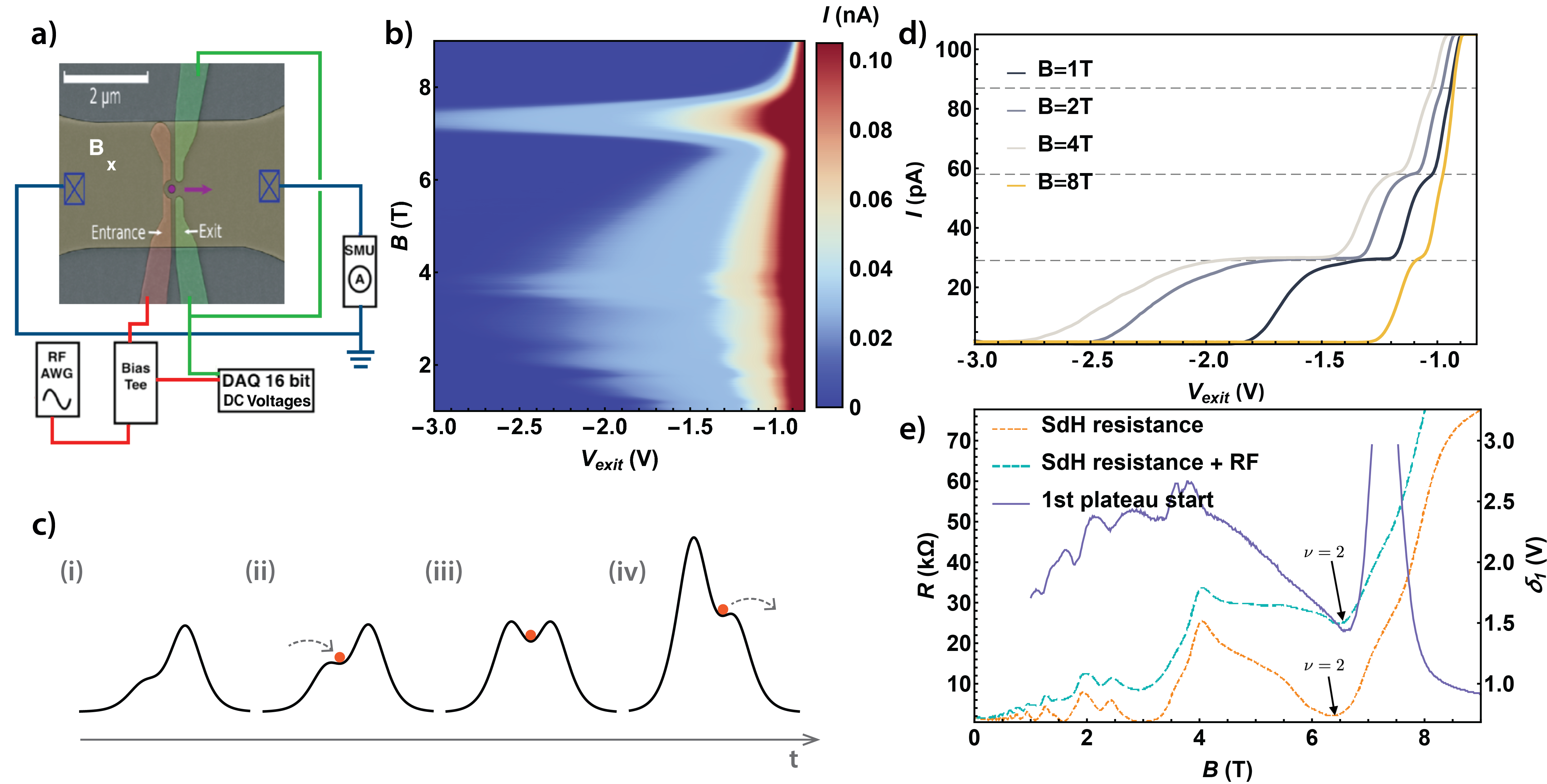
The SEM image of the pump and the schematic of the experiment are shown in Fig.1a, with further details given in the Methods section. The principle of device operation is illustrated in Fig.1c.
The time evolution panels (i) - (iv) show a cross-section of the spatial 3D potential created by the gates. At the beginning of the cycle (i), the left entrance barrier is low and the dot potential profile has a single maximum. As the entrance barrier potential increases (ii), a local minimum appears in the potential, creating confined states, which can be occupied by electrons from the source (capture stage). With further increase (iii), the confined states become isolated from the source and move with the evolution of the potential profile. Finally (iv), the confined states are destroyed and electrons are ejected into the drain.
The number of pumped electrons per cycle can be fine-tuned at constant RF frequency and amplitude by both the DC gate voltages. Fig.1d shows four pumping traces at different magnetic fields for a fixed entrance gate offset voltage and RF parameters. The pumped current evolves as a function of the exit gate voltage , with the integer number of pumped electrons increasing as the DC voltage on the exit barrier is made more positive (the barrier is lowered).
Fig.1b shows a pumpmap of the current as a function of and magnetic field Wright et al. (2010) with the entrance gate DC voltage fixed at mV, the source-drain bias mV, and the RF amplitude and frequency mV and MHz. On observation, the plateau lengths depend strongly on the magnetic field, and the general trend over the field T is towards plateau lengthening, in agreement with previous studiesWright et al. (2008); Kaestner et al. (2009). The plateau length dependence is however non-monotonic, but instead oscillatory, including a dramatic resonance peak at around T.
These oscillations are reminiscent of magnetic field dependencies seen in the Shubnikov-de Haas effect. We study the SdH effect in the pump by measuring the longitudinal resistance of the device as a function of magnetic field, first with the finger gate grounded (Fig.1e, orange) and then with an RF signal on the finger gate (Fig.1e, turquoise) with the parameters of the RF signal set as used during pumping. These SdH plots in the quantum Hall regime are compared to the exit gate voltage corresponding to the start of the first pumping plateau (current is at of the expected plateau value, see Eq.1) as a function of magnetic field (Fig.1e, blue).
The SdH plot without the RF signal differs from assessment measurements in the same wafer with a standard Hall bar. This difference can be attributed to the geometry of the mesa in the pump deviating substantially from a standard Hall bar geometry. The inclusion of Ti/Au gates as well as the fabrication process itself also affect the wafer, altering the electron density and mobility. The application of the RF signal further influences the magnetic field dependence of the device resistance, however both retain the general peak structure of the signature SdH.
As the magnetic field oscillations in the SdH effect originate in the Landau quantisation of the electron states, we make the conjecture that similarly, the pumping of electrons depends on the population of the density of states in the source side of the pump. The rest of the work expands on this assumption.
III Theoretical model
III.1 Motivations and criteria for the model
A single-electron pump is a complex open quantum system with many aspects which make it a serious challenge for theoretical descriptionPyurbeeva, Mol, and Gehring (2022): both particle and energy exchange being present, a time-dependent Hamiltonian, multiple competing time-scales, out-of-equilibrium conditions and multi-electron processes. Combinations of these are studied in topics such as driven quantum dots, for applications such quantum heat engines or refrigeratorsJuergens et al. (2013); Hino and Hayakawa (2021); Monsel et al. (2022); Monsel, Schulenborg, and Splettstoesser (2023), or far-from-equilibrium thermodynamics in nanodevicesPyurbeeva, Thomas, and Mol (2023).
However, single-electron pumps exhibit additional complexity due to qualitative changes, such as the creation and destruction of confined states, and strong system-bath coupling associated with it, alongside quantitative changes like cycling of addition energy. Recent researchSchulenborg et al. (2023) has focused on dynamical analysis from an open quantum system perspective, including a study on two-electron emission processes from a quantum dot, however such approaches are computationally involved. Our investigation, focusing on the capture side of the cycle and incorporating a magnetic field, takes a more qualitative and intuitive approach.
The main result of the UDC model is a double-exponential fitting equation for the pumping curvesHowe et al. (2021):
| (1) |
where subscript is the plateau number, is the plateau’s lever arm, and – its position in . These parameters act as a fingerprint of the pump device, allowing for the pump comparison and optimisationKashcheyevs and Kaestner (2010).
Equation 1 gives a good fit to the experimental data in a wide variety of electron pump geometriesHowe et al. (2021), but despite later expansionsKashcheyevs and Timoshenko (2012, 2014) on the model, it does not link explicitly to any key physical parameters such a temperature, B field, RF signal amplitude, and frequency.
Our experimental data (Fig.1b) provides the first systematic high-precision study of the dependence of the pumping on an external parameter, the magnetic field. We now construct a model to describe our findings.
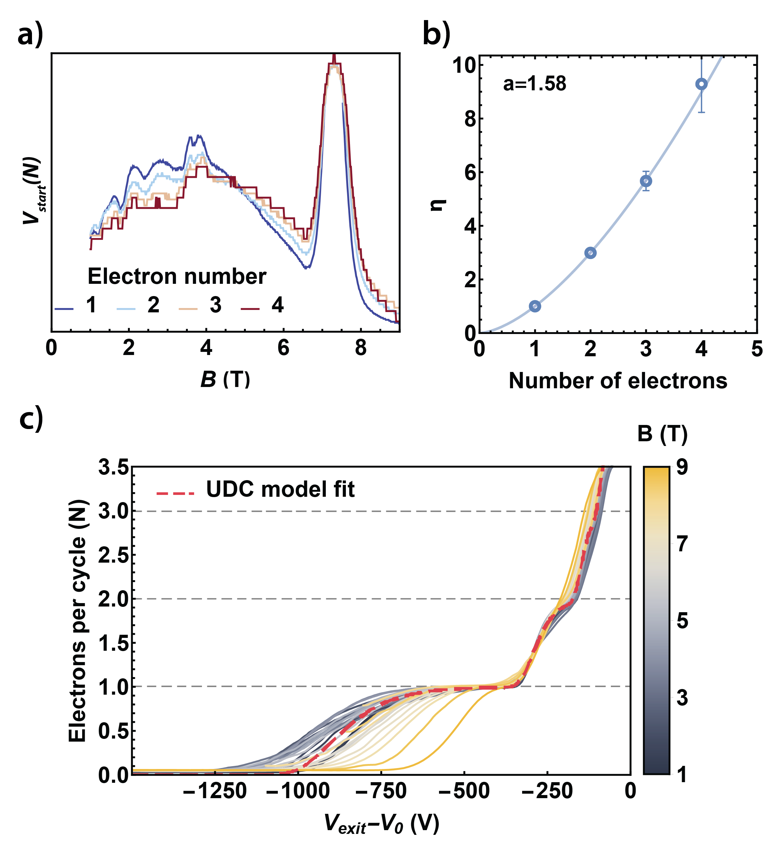
In Fig.2a the starting voltages (corresponding to the current reaching of the true integer plateau) for (blue) to (red) are given as a function of . These line scans were taken from Fig.1b and linearly scaled by a factor of (), shown in Fig.2b. The scaling factors follow a power law in with the power .
The fact that – coincide up to a linear transformation (Fig.2a), indicates that there is a single parameter governing the overall length of the pumping trace, rather than the start of each plateau having separate magnetic field dependencies. Fig.2c shows the pumping traces at different magnetic fields stretched by the length factor determined in Fig.2a, further supporting this claim, and showing a “true” pumping trace inherent to the device.
The length function , bears a strong resemblance to the SdH oscillations of longitudinal resistance of the 2DEG which is proportional to the density of states at the Fermi-level as discussed previously (Fig.1e). We can conclude that the pumping process not only depends on the density of states in the source electrode, but on the density of states at a single energy – if was governed by electron exchange processes at different energies, it would be a convolution of at different values of , and the contributions from different Landau levels would be washed out. The sharp Landau level signatures observed indicate that the entire pumping effect is determined by exchange processes confined to a very narrow energy window.
III.2 The 0-DIP model and dot parameters
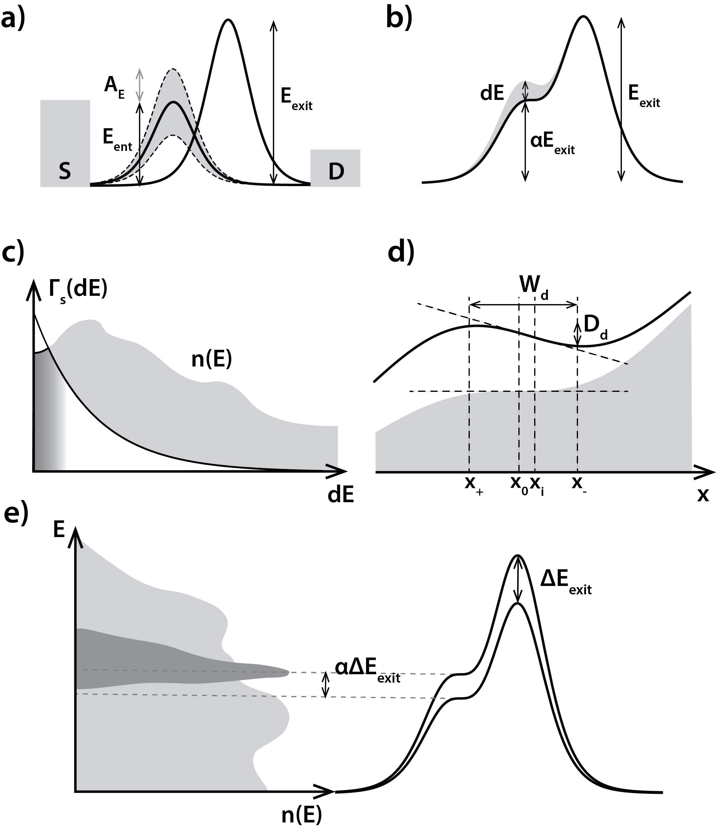
We now propose a physical model based on our observations. We utilise a 1D system and describe the electron energy profiles created by the application of the voltages and to the entrance and exit electrodes as smooth differentiable peak functions and with continuous first and second derivatives. The maximal values of the electron energies are and , which depend linearly on the voltages applied (Fig.3a).
If the peaks are sufficiently close to one another, for every value of there exist two values of for which the total potential profile exhibits an inflection point with a zero derivative, with the inflection points on the source side for low and drain side for high . We call the former configuration the 0-DIP potential (Fig.3b). The value of at the 0-DIP potential is proportional to , where we define the proportionality coefficient as .
The significance of the 0-DIP potential is that it approximately separates two configurations of the dynamically defined dot – that with no confined electron states (), and that other containing one or multiple confined states. We assume that confined states form soon after passes the 0-DIP potential. A crucial point in our model is that a further increase of with the application of the RF signal leads to a rapid reduction in the tunnel coupling between the now-formed dot and the source (Fig.3c). After a small increment in entry barrier height, the dot is completely isolated, not only from the drain, but also from the source (grey shaded profile in Fig.3b).
The value of is assumed small in comparison to the characteristic broadened width of the Landau levels. This assumption contributes to the explanation of the oscillatory behaviour of the pumped current vs magnetic field in Fig.1b and is a requirement of our model.
To demonstrate the validity of this 0-DIP model, we investigate the evolution of the geometry of the quantum dot during the pump cycle. We define two fundamental dimensions of the dot: the width of the entrance potential barrier and the depth of the dot (Fig.3d) and model the change in these dimensions as a function of in a one-dimensional system. Analytically making use of Taylor expansion (see Methods) we find the following two expressions for the dot parameters:
| (2) |
While the exact form of the dependence will be different for a two-dimensional case and will depend on the geometry of the electrodes, qualitatively it will follow the 1D case, with the barrier height and width increasing with and decreasing with . The effect of dot size on pumping can be seen in the well-known universal feature of the pumping traces – less negative (lower ) leading to more electrons being pumped per cycle, which intuitively agrees with a geometrically larger quantum dot. Additionally, the increase of with supports the initial assumption of the dot only being coupled to the source in a narrow energy window, as the coupling to the source depends exponentially on (Fig.3c).
IV Data analysis – density of states and capture energy
We now apply the developed 0-DIP model to the experimental data. This allows us to determine certain numerical properties of the pumping mechanism in high fields and validate our model.
The electron pump, defined in a quasi one-dimensional restriction etched into a 2DEG AlGaAs mesa with multiple Ohmic contacts, allowed for routine Quantum Hall and SdH measurements to determine the electron density of the pump mesa. Initially, all gates were grounded, and then measurements were repeated with the finger gate oscillating at the same frequency and amplitude used during the pump’s operation. These measurements revealed an electron density of m-2, which corresponds favourably with what was measured by the growers ( m-2) in the Cavendish Laboratory on the stock wafer before any fabrication on the wafer.
From the SdH oscillations and measured electron density we were in a position to determine the filling factors . We observe that the final minimum in the SdH data (Fig.1e orange), where the Fermi level is in a localised state corresponds with all the electrons in the first Landau level (, including spin). This aligns with the minimum in the pumping data at ,T, occurring just before the onset of the significant resonance peak at ,T (Fig.1e). The last minimum in the SdH data shows a stronger coincidence with the minima in the pumped data if the RF gate when measuring the SdH was switched on.
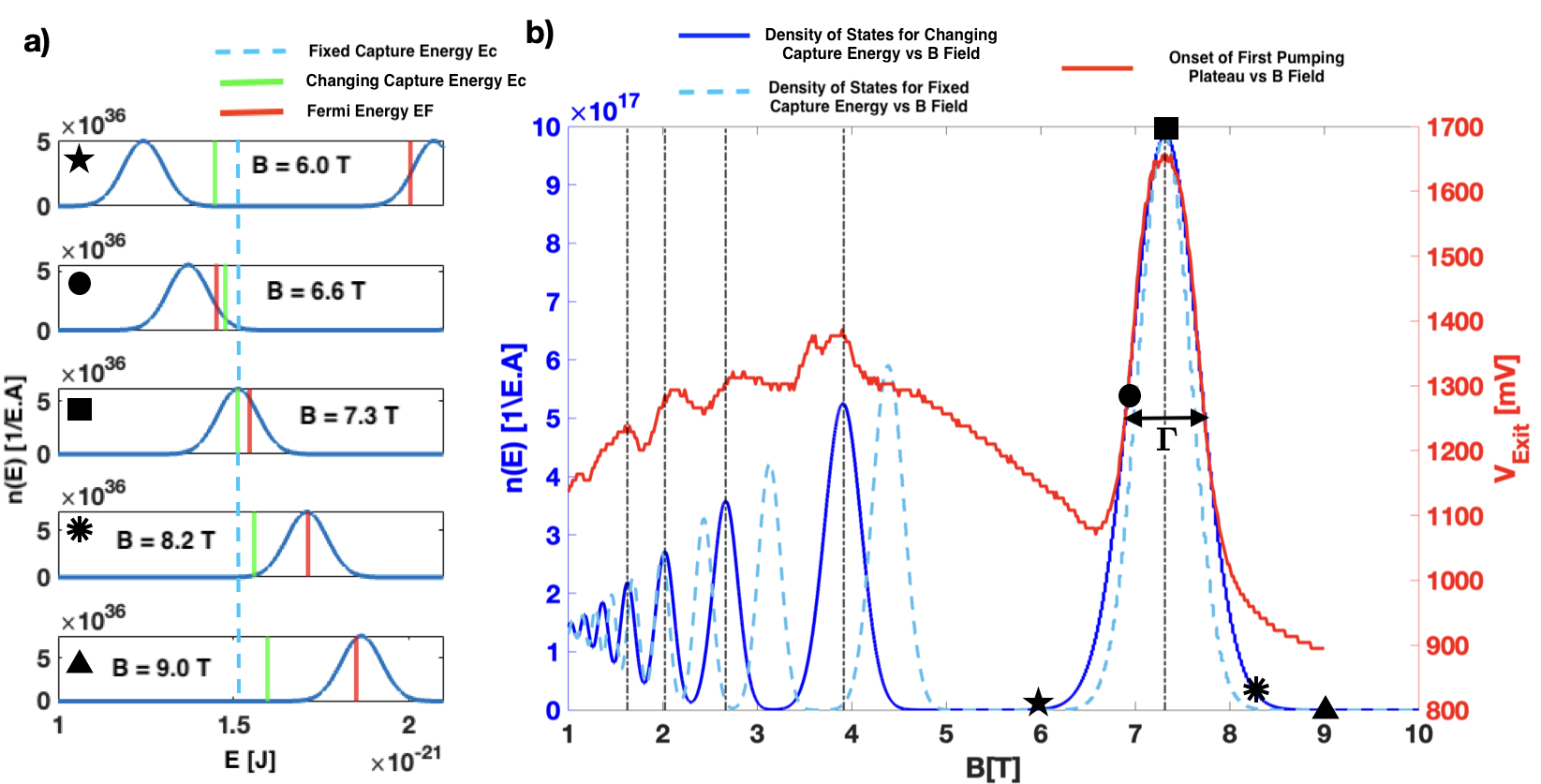
Using the above, we then simulated using code written in Matlab, the movement of the Landau levels, and the Fermi energy governed by the determined density of electrons above as the magnetic field was changed. We focused initially on the region of the resonance peak at B values of T, T, T, T and T.
First we determined the Landau level broadening (fwhm), a requirement for observing the quantum Hall effectPotts et al. (1996), which is given by , where is the quantum lifetime. is determined from the resonance peak (red line, Fig.4b), which as previously discussed in the 0-DIP model, corresponds to the dot probing the Landau level with filling factor (including spin) as the capture energy changes monotonically as B is swept (Fig.4a). We obtained ,J, corresponding to a lifetime of ,ps. This lifetime, the mean time a carrier remains in a momentum eigenstate before scatteringQian et al. (2017), is an order of magnitude shorter than typical time scales from standard quantum Hall measurementsMartin et al. (1988). In the pumping regime, introducing the RF signal disrupts the system, increasing scattering and shortening the quantum lifetime. Further investigations will explore the RF frequency and amplitude’s impact on .
The movement of the Landau levels (black peaks) and Fermi level (red lines) are shown in the selection of plots in Fig.4a with the width of the Landau peaks as determined above. At the resonance peak at T the Fermi level despite not being centred in the lowest Landau level is contained within it.
With this finding we then determined the capture energy of the electrons. We start with the assumption that at the resonance peak at T, the capture energy given by the green line is at the centre of the first Landau level for T(Fig.4a ). It is also below the Fermi level given in red, which is essential as there are no electrons for pump capture at energies above the source lead Fermi level.
We then modelled two different scenarios. First, we assumed that the capture energy of the electrons during the pump cycle does not change as a function of magnetic field and we pinned the capture energy at the centre of the lowest Landau level J for all B as shown in Fig. 4a by the dotted turquoise line. We then monitored the change in the density of states at this fixed capture energy as a function of B which is then plotted as the dotted turquoise line in Fig.4b. Second, we assumed that the capture energy is changing as a function of magnetic field linearly. We scaled the capture energy at T ( J) over the full B field from T to T. The capture energy therefore changed by J over the full range of B field. The plot of the density of states as the capture energy was changed from J to J in step with the change in B from T to T, in multiples of T is shown by the dark blue solid trace in Fig.4b).
From these two plots we see a much stronger coincidence between the dark blue and red onset pumping curve allowing us to conclude the capture energy of the electrons changes, albeit slightly, over the full magnetic field sweep.
V Conclusion
Our experimental data of single-electron pumping through a split-gate finger-gate quantum dot at high magnetic fields demonstrates oscillatory behaviour reminiscent of the SdH effect. The inclusion of a split-gate on the exit side of the quantum dot allows for an increase in gate resolution due to a lower lever-arm term. This, with the change in potential profile on the exit side of the quantum dot from a simple Gaussian to a saddle-point potential, has allowed for further probing of the dynamics of these on-demand electron sources. Our analysis together with a new pumping model based on the foundations of the UDC model has allowed for the first reported direct measurement of the capture energy, the broadening of Landau levels in such pump devices and therefore the quantum lifetime of the pumped electrons. This demonstration of single electron pumping in the quantum Hall regime, where electrons are captured from specific Landau levels, shows the capture energy to be independent of the exit gate DC voltage for fixed B field, but a change in the capture energy is observed as the B field itself is varied.
Future work will explore further the frequency and temperature dependence of pumps operating in this regime as well the ejection energy of the pumped electrons.
Acknowledgements
This work was supported by the UK Engineering Physical Sciences Research Council, grants EP/K040359/1 and EP/R029075/1, the National Research Foundation of South Africa. J.A.M. acknowledges a UKRI Future Leaders Fellowship, grant no. MR/X023125/1.
Author contributions
E.P developed the theoretical model, produced data plots, interpreted the data and contributed to the drafting of the paper. M.D.B ran the experiment, carried out the simulation work, interpreted the data and contributed to the drafting of the paper. Both E.P and M.D.B contributed equally. H.H. designed and processed the devices. J.A.M contributed to data interpretation. T.M carried out the e-beam lithography. H.E.B and D.A.R developed and grew the GaAs/AlGaAs heterostructures used. M.P. provided support, references, and useful discussions. All authors reviewed the manuscript.
Methods
V.1 Fabrication and Experiment Setup
Our device comprises a single-electron pump with two Ti/Au gates in a finger-gate split-gate geometry (red and green in Fig.1a respectively). Only the entrance gate, in our the case the finger-gate, is coupled directly to the Agilent RF signal generator. The pumped current is measured via a Keithley 6430 Source-Measure unit capable of measuring at the femto-ampere level. DC voltages are applied to the gates via multiple channel 16 bit DAQs. Unlike the earlier pump configurations, in which oscillating voltages have been applied to both the exit and entrance gateFujiwara et al. (2004); Blumenthal et al. (2007), we follow a later protocolFujiwara, Nishiguchi, and Ono (2008); Kaestner et al. (2008), in which the potential of the exit gate is held constant during the pump cycle, and the entrance gate oscillates due to the RF signal added to the constant potential via a bias T. The gates were fabricated using electron beam lithography with Ti/Au thermally evaporated. The entrance finger gate (red) and split gate (green) are used to define the QD entrance and exit gate respectively. DC voltages were applied to all gates using a NI2969 cDAQ with the RF signal coupled to the exit gate via a bias tee. The RF source used was a HP E4400B driving a simple sinusoidal wave.
The device was fabricated on a two-dimensional high mobility GaAs/AlxGa1-xAs Si-doped electron gas system grown using molecular beam epitaxy. The 2DEG was formed 90 nm below the surface (10 nm GaAs cap, 40 nm Si-doped GaAs/AlxGa1-xAs, 40 nm GaAs/AlxGa1-xAs spacer, and GaAs substrate with a carrier density cm-2 and mobility cm2/Vs). The 2DEG channel pattern was defined using electron-beam lithography (EBL) and etched to a depth of 40 nm using wet chemistry. The split gate has a width and gap of nm, whilst the finger gate a width of nm. The pitch of the gates are nm. The sample was loaded into a Leiden Cryogenics dilution fridge with a base temperature of mK and a T superconducting magnet. The pumped current was measured using a Keithley 6430 source measure unit (SMU), which was connected to the drain side of the pump. The source side was grounded.
V.2 Dot parameters – analytical consideration
We find the dependence of the quantum dot parameters and – width of the potential barrier and the dot depth in a 1D case – shortly after the system has passed the 0-DIP configuration. The potential profile is the sum of the potential profiles of both electrodes:
| (3) |
where and are the normalised functions of the potentials creates by each of the electrodes independently, we assume they are smooth, differentiable, with a simple peak, and .
In the 0-DIP configuration, . If is the inflection point, then the first and second derivatives of the potential profile in it are equal to zero:
| (4) |
Shortly past the 0-DIP configuration, , the derivatives at the same point are:
| (5) |
In this case (see Fig.3d), the potential has three special points – the new inflection point , the local maximum and the local minimum . Assuming that is small and the special points lie within a small vicinity of the former inflection point we find the distance between the new and the former inflection points in the Taylor expansion. Postulating , we arrive at:
| (6) |
At the new inflection point, to the first order,
| (7) |
Finally, we find the distance between the new inflection point and the maximum and minimum and . Setting
| (8) |
we arrive at:
| (9) |
We set , the distance between the local minimum and maximum as the characteristic size of the dot, which is equal to the width of the potential barrier; and the depth of the dot, or the height of the barrier can be found as:
| (10) |
which yields:
| (11) |
The final dependence on the external parameters has the form:
| (12) |
.
References
- Pekola et al. (2013) J. P. Pekola, O.-P. Saira, V. F. Maisi, A. Kemppinen, M. Möttönen, Y. A. Pashkin, and D. V. Averin, Rev. Mod. Phys. 85, 1421 (2013).
- Keller et al. (1997) M. Keller, J. Martinis, A. Steinbach, and N. Zimmerman, Instrumentation and Measurement, IEEE Transactions on 46, 307 (1997).
- Bäuerle et al. (2018) C. Bäuerle, D. Christian Glattli, T. Meunier, F. Portier, P. Roche, P. Roulleau, S. Takada, and X. Waintal, Reports Prog. Phys. 81, 056503 (2018), arXiv:1801.07497 .
- Kaneko, Nakamura, and Okazaki (2016) N.-H. Kaneko, S. Nakamura, and Y. Okazaki, Measurement Science and Technology 27, 032001 (2016).
- Dupont-Ferrier et al. (2013) E. Dupont-Ferrier, B. Roche, B. Voisin, X. Jehl, R. Wacquez, M. Vinet, M. Sanquer, and S. De Franceschi, Phys. Rev. Lett. 110, 136802 (2013).
- DiVincenzo and IBM. (2000) D. DiVincenzo and IBM., Fortschritte der Physik 48 (2000), 10.1002/1521-3978(200009)48:9/113.0.CO;2-E.
- Wright et al. (2009) S. J. Wright, M. D. Blumenthal, M. Pepper, D. Anderson, G. A. C. Jones, C. A. Nicoll, and D. A. Ritchie, Phys. Rev. B 80, 113303 (2009).
- Maisi et al. (2009) V. Maisi, Y. Pashkin, S. Kafanov, J.-S. Tsai, and J. Pekola, New Journal of Physics 11 (2009), 10.1088/1367-2630/11/11/113057.
- Giblin et al. (2019) S. P. Giblin, A. Fujiwara, G. Yamahata, M.-H. Bae, N. Kim, A. Rossi, M. Möttönen, and M. Kataoka, Metrologia 56, 044004 (2019).
- Yamamoto et al. (2012) M. Yamamoto, S. Takada, C. Bäuerle, K. Watanabe, A. D. Wieck, and S. Tarucha, Nature Nanotechnology 7, 247 (2012).
- Ji et al. (2003) Y. Ji, Y. Chung, D. Sprinzak, M. Heiblum, D. Mahalu, and H. Shtrikman, Nature 422, 415 (2003).
- Ubbelohde et al. (2015) N. Ubbelohde, F. Hohls, V. Kashcheyevs, T. Wagner, L. Fricke, B. Kästner, K. Pierz, H. W. Schumacher, and R. J. Haug, Nature Nanotechnology 10, 46 (2015).
- Gumbs et al. (2009) G. Gumbs, D. Huang, M. Blumenthal, S. J. Wright, M. Pepper, and Y. Abranyos, Semiconductor Science and Technology 24 (2009), 10.1088/0268-1242/24/11/115001.
- Fletcher et al. (2013) J. D. Fletcher, P. See, H. Howe, M. Pepper, S. P. Giblin, J. P. Griffiths, G. A. C. Jones, I. Farrer, D. A. Ritchie, T. J. B. M. Janssen, and M. Kataoka, Phys. Rev. Lett. 111, 216807 (2013).
- Blumenthal et al. (2023) M. D. Blumenthal, D. Mahony, S. Ahmad, D. Gouveia, H. Howe, H. E. Beere, T. Mitchel, D. A. Ritchie, and M. Pepper, EPJ Quantum Technol. 10, 46 (2023).
- Ubbelohde et al. (2023) N. Ubbelohde, L. Freise, E. Pavlovska, P. G. Silvestrov, P. Recher, M. Kokainis, G. Barinovs, F. Hohls, T. Weimann, K. Pierz, and V. Kashcheyevs, Nature Nanotechnology 18, 733 (2023).
- Brange and Flindt (2023) F. Brange and C. Flindt, Nature Nanotechnology 18, 696 (2023).
- Blumenthal et al. (2007) M. D. Blumenthal, B. Kaestner, L. Li, S. Giblin, T. J. B. M. Janssen, M. Pepper, D. Anderson, G. Jones, and D. A. Ritchie, Nat. Phys. 3, 343 (2007).
- Kaestner et al. (2008) B. Kaestner, V. Kashcheyevs, S. Amakawa, M. D. Blumenthal, L. Li, T. J. B. M. Janssen, G. Hein, K. Pierz, T. Weimann, U. Siegner, and H. W. Schumacher, Phys. Rev. B 77, 153301 (2008), arXiv:0707.0993 .
- Kaestner and Kashcheyevs (2015) B. Kaestner and V. Kashcheyevs, Reports Prog. Phys. 78, 103901 (2015), arXiv:1412.7150 .
- Yamahata, Nishiguchi, and Fujiwara (2014) G. Yamahata, K. Nishiguchi, and A. Fujiwara, Nature communications 5, 5038 (2014).
- Yamahata and Fujiwara (2024) G. Yamahata and A. Fujiwara, Journal of Applied Physics 135 (2024), 10.1063/5.0179374.
- Moraru et al. (2007) D. Moraru, Y. Ono, H. Inokawa, and M. Tabe, Phys. Rev. B - Condens. Matter Mater. Phys. 76, 1 (2007).
- Roche et al. (2013) B. Roche, R.-P. Riwar, B. Voisin, E. Dupont-Ferrier, R. Wacquez, M. Vinet, M. Sanquer, J. Splettstoesser, and X. Jehl, Nature Communications 4, 1581 (2013).
- Lansbergen, Ono, and Fujiwara (2012) G. P. Lansbergen, Y. Ono, and A. Fujiwara, Nano Letters 12, 763 (2012).
- Tettamanzi, Wacquez, and Rogge (2014) G. Tettamanzi, R. Wacquez, and S. Rogge, New Journal of Physics 16, 063036 (2014).
- Kashcheyevs and Kaestner (2010) V. Kashcheyevs and B. Kaestner, Phys. Rev. Lett. 104, 1 (2010), arXiv:0901.4102 .
- Rossi et al. (2018) A. Rossi, J. Klochan, J. Timoshenko, F. E. Hudson, M. Möttönen, S. Rogge, A. S. Dzurak, V. Kashcheyevs, and G. C. Tettamanzi, Nano Lett. 18, 4141 (2018), arXiv:1803.00791 .
- Howe et al. (2021) H. Howe, M. Blumenthal, H. E. Beere, T. Mitchell, D. A. Ritchie, and M. Pepper, Appl. Phys. Lett. 119, 153102 (2021).
- Wright et al. (2008) S. J. Wright, M. D. Blumenthal, G. Gumbs, A. L. Thorn, M. Pepper, T. J. Janssen, S. N. Holmes, D. Anderson, G. A. Jones, C. A. Nicoll, and D. A. Ritchie, Phys. Rev. B - Condens. Matter Mater. Phys. 78, 1 (2008), arXiv:0811.0494 .
- Kaestner et al. (2009) B. Kaestner, C. Leicht, V. Kashcheyevs, K. Pierz, U. Siegner, and H. W. Schumacher, Appl. Phys. Lett. 94, 012106 (2009), arXiv:0811.1121 .
- Leicht et al. (2010) C. Leicht, B. Kaestner, V. Kashcheyevs, P. Mirovsky, T. Weimann, K. Pierz, and H. W. Schumacher, Phys. E Low-Dimensional Syst. Nanostructures 42, 911 (2010), arXiv:0909.2778 .
- Hanief et al. (2024) N. Hanief, M. Blumenthal, H. Howe, H. Beere, T. Mitchell, D. Ritchie, and M. Pepper, Scientific African 24, e02150 (2024).
- Wright et al. (2010) S. Wright, A. Thorn, M. Blumenthal, S. Giblin, M. Pepper, T. Janssen, M. Kataoka, J. Fletcher, G. Jones, C. Nicoll, G. Gumbs, and D. Ritchie, Journal of Applied Physics - J APPL PHYS 109 (2010), 10.1063/1.3578685.
- Pyurbeeva, Mol, and Gehring (2022) E. Pyurbeeva, J. A. Mol, and P. Gehring, Chem. Phys. Rev. 3, 041308 (2022), arXiv:2206.05793 .
- Juergens et al. (2013) S. Juergens, F. Haupt, M. Moskalets, and J. Splettstoesser, Phys. Rev. B - Condens. Matter Mater. Phys. 87, 1 (2013), arXiv:1303.5225 .
- Hino and Hayakawa (2021) Y. Hino and H. Hayakawa, Phys. Rev. Res. 3, 013187 (2021), arXiv:2003.05567 .
- Monsel et al. (2022) J. Monsel, J. Schulenborg, T. Baquet, and J. Splettstoesser, Phys. Rev. B 106, 035405 (2022), arXiv:2202.12221 .
- Monsel, Schulenborg, and Splettstoesser (2023) J. Monsel, J. Schulenborg, and J. Splettstoesser, Eur. Phys. J. Spec. Top. 123 (2023), 10.1140/epjs/s11734-023-00969-4.
- Pyurbeeva, Thomas, and Mol (2023) E. Pyurbeeva, J. O. Thomas, and J. A. Mol, Mater. Quantum Technol. 3, 025003 (2023), arXiv:2212.10600 .
- Schulenborg et al. (2023) J. Schulenborg, J. D. Fletcher, M. Kataoka, and J. Splettstoesser, 1, 1 (2023), arXiv:2303.15436 .
- Kashcheyevs and Timoshenko (2012) V. Kashcheyevs and J. Timoshenko, Phys. Rev. Lett. 109, 216801 (2012), arXiv:1205.3497 .
- Kashcheyevs and Timoshenko (2014) V. Kashcheyevs and J. Timoshenko, CPEM Dig. (Conference Precis. Electromagn. Meas. , 536 (2014), arXiv:1402.0637 .
- Potts et al. (1996) A. Potts, R. Shepherd, W. G. Herrenden-Harker, M. Elliott, C. L. Jones, A. Usher, G. A. C. Jones, D. A. Ritchie, E. H. Linfield, and M. Grimshaw, Journal of Physics: Condensed Matter 8, 5189 (1996).
- Qian et al. (2017) Q. Qian, J. Nakamura, S. Fallahi, G. C. Gardner, J. D. Watson, S. Lüscher, J. A. Folk, G. A. Csáthy, and M. J. Manfra, Phys. Rev. B 96, 035309 (2017).
- Martin et al. (1988) K. Martin, R. Higgins, J. Rascol, H. Yoo, and J. R. Arthur, Surface Science 196, 323 (1988).
- Fujiwara et al. (2004) A. Fujiwara, N. M. Zimmerman, Y. Ono, and Y. Takahashi, Appl. Phys. Lett. 84, 1323 (2004).
- Fujiwara, Nishiguchi, and Ono (2008) A. Fujiwara, K. Nishiguchi, and Y. Ono, Appl. Phys. Lett. 92 (2008), 10.1063/1.2837544.