]These authors contributed equally]These authors contributed equally
MKIDGen3:
Energy-Resolving, Single-Photon-Counting MKID Readout on an RFSoC
Abstract
Microwave Kinetic Inductance Detectors (MKIDs) are superconducting detectors capable of single-photon counting with energy resolution across the ultraviolet, optical, and infrared (UVOIR) spectrum with microsecond timing precision. MKIDs are also multiplexable, providing a feasible way to create large-format, cryogenic arrays for sensitive imaging applications in biology, astronomy, and quantum information. Building large, cryogenic MKID arrays requires processing highly-multiplexed, wideband readout signals in real time; a task that has previously required large, heavy, and power-intensive custom electronics. In this work, we present the third-generation UVOIR MKID readout system (Gen3) which is capable of reading out twice as many detectors with a fifth the weight and power and an order of magnitude less volume and cost-per-pixel as compared to the previous system. Gen3 leverages the Xilinx RFSoC4x2 platform to read out 2048, 1 MHz MKID channels per board. The system takes a modern approach to FPGA design using Vitis High-Level Synthesis (HLS) to specify signal processing blocks in C/C++, Vivado ML Intelligent Design Runs (IDR) to inform implementation stragety and close timing, and Python Productivity for ZYNQ (PYNQ) to simplify interacting with and programming the FPGA using Python. This design suite and tool flow allows general users to contribute to and maintain the design and positions Gen3 to rapidly migrate to future platforms as they become available. In this work, we describe the system requirements, design, and implementation. We also provide performance characterization details and show that the system achieves detector-limited resolving power in the case of few readout tones and minimal degradation with all 2048 tones. Planned upgrades and future work are also discussed. The Gen3 MKID readout system is fully open-source and is expected to facilitate future array scaling to megapixel-sized formats and increase the feasibility of deploying UVOIR MKIDs in space.
I Introduction
Microwave Kinetic Inductance Detectors (MKIDs) are promising superconducting detectors with applications for highly-sensitive photon measurements such as those needed in quantum computing, biological imaging, and astrophysical observations Todaro et al. (2021); Mariantoni et al. (2011); Xia et al. (2021); Niwa et al. (2017); Zmuidzinas (2012); Mazin (2009). MKIDs are able to detect the energy and arrival time of single photons using the changes induced in the kinetic inductance of superconducting materials by incident photons Day et al. (2003). This operating principle allows for single-photon counting with zero read noise or dark current across ultraviolet, optical, and infrared (UVOIR) wavelengths with microsecond timing precisionZobrist et al. (2019, 2022). MKIDs also natively support multiplexing many detectors per readout line using frequency-division multiplexing (FDM)–a technique that will be discussed more in Sec. II.2. FDM provides a feasible means of scaling MKIDs to large cryogenic arrays suitable for high-resolution imaging.
The focus of our group is to develop UVOIR MKIDs into fast, energy-resolving, single-photon-counting cameras for scientific imaging and spectroscopy. We have successfully deployed a twenty-kilopixel UVOIR MKID array in the MKID Exoplanet Camera (MEC) Walter et al. (2020) and have demonstrated several high-contrast imaging astronomy results Steiger et al. (2021); Swimmer et al. (2022). We are developing an echelle spectrograph testbench Iii et al. (2022) and are also pursing science applications in quantum information and biological imaging.
Progress has been slowed in part by the current, second-generation MKID digital readout system (hereafter Gen2) which is excessively large, cumbersome, and power-hungry by modern standards Fruitwala et al. (2020). Gen2 will not scale for larger ground-based arrays and is not suitable for future space-based missions. Gen2 also relies on obsolete hardware and tools, making it exceedingly difficult to update and to integrate modern advances in photon signal detection.
To alleviate these challenges, we have created the next generation MKID digital readout which is capable of reading out twice as many MKIDs per board with a fraction of the weight, volume, and power of the previous system. A key advancement is the migration to the Xilinx RFSoC platform with FPGA-integrated, high-speed analog-to-digital and digital-to-analog converters (ADCs/DACs). The integrated platform provides a dramatic reduction in power and device footprint that will enable future high-altitude missions and ease system scaling. We also leveraged modern FPGA programming tools including Vitis High-Level Synthesis (HLS), which synthesizes C++ code to FPGA-specific hardware description language, and Python Productivity for Zynq (PYNQ), which facilitates interacting with the FPGA through Python. These tools are more accessible to scientists and astronomers without specialized knowledge of FPGA design and create a system which is easier to maintain and upgrade.
In this work, we discuss the system design, implementation, and performance. We include a brief introduction to MKID readout in Sec. II to provide context for the requirements outlined in Sec. III. Next, we describe our approach to system design in Sec. IV and describe the FPGA implementation including our use of HLS and our timing closure strategy. We provide performance characterization for the system in loopback in Sec. V and include detailed studies of actual cryogenic MKID readout performance in Sec. V.4. We conclude with a discussion of the system performance in Sec. VI and describe future directions and next steps. The MKID digital readout described here is fully open-source and available on GitHub under a GPLv3.0 license111https://github.com/MazinLab/MKIDGen3.
II MKID Readout
MKID readout is a rich topic with a large body of prior work dedicated to the underlying physics and improving detector performance Gao (2008); Mazin (2005); Zobrist (2022). Here we provide a brief review of core MKID readout signals and the strategy underpinning the digital design. We include a high-level description of MKID setup and operation to clarify goals, terminology, and analysis used in the remainder of this work.
II.1 MKIDs as Superconducting Resonators
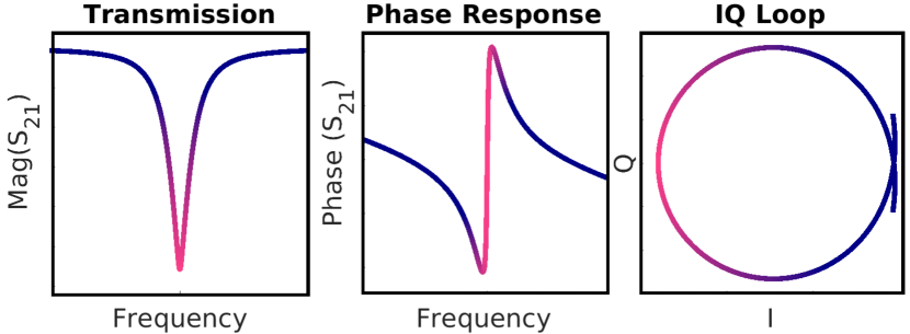
Each MKID pixel is a superconducting LC resonator. Our designs target resonance frequencies in 4-8 GHz due to commercial availability of cryogenic low-noise amplifiers in this band. MKIDs are read out using a homodyne scheme where the signal of interest is a modulation on the readout tone and can be represented as a complex signal. This signal is acquired by down-converting the readout tone to 0 Hz. A simulated MKID frequency response is plotted in Fig. 1. The IQ loop (Fig. 1, right) contains all the information needed to determine the correct readout frequency, phase offset, and loop center coordinates for photon readout, and as such characterizing each MKID IQ loop is an important setup function for MKID readout systems.
II.2 Frequency-Division Multiplexing
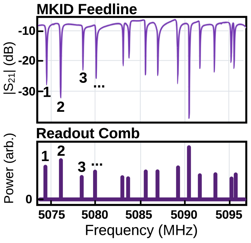
MKIDs use frequency-division multiplexing to thread many superconducting resonators on a single readout line. This technique allows MKID readout signals to share a microwave feedline, conserving cryogenic heat load and promoting the creation of large arrays. A sample transmission from a real MKID feedline is shown in Fig. 2, (top). Each resonator is fabricated with a different resonance frequency, allowing each resonator to be addressed by its unique resonance. We target 2048 resonators with a spacing of 2 MHz but lose 10% to 40% of pixels due to resonator collisions and other fabrication process uncertainties. More details on MKID array fabrication are provided in referencesSzypryt et al. (2016); Coiffard et al. (2020); Mazin (2020). Each feedline represents a base unit for a full MKID array with each feedline being an imperfect copy of the others. In this work, references to multi-MKID readout refer to a single feedline with the understanding that a high-level control program can aggregate data from each feedline to create array-level data products.
II.3 MKID Feedline Setup
After fabrication, the precise locations of the pixels and their optimal readout parameters are unknown. The digital readout uses a reprogrammable local oscillator (LO) to sweep a comb of uniform tones across the 4-8 GHz feedline while collecting transmission data, similar to a vector network analyzer. The frequency sweep is repeated at different powers and the resulting IQ loops are used to determine the optimal readout frequency, power, phase offset, and loop center coordinates for each MKID. The readout powers and frequencies are used to generate a customized DAC output consisting of a superposition of the readout tones (see Fig. 2, bottom). The phase offsets and loop center coordinates are used to rotate and center each IQ loop in order to standardize the photon response curve. After the optimal readout tones and powers have been used to generate the readout waveform and the IQ loops have been rotated and centered, the device is ready for photon readout.
II.4 Photon Readout
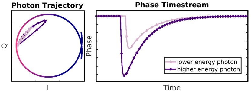
When a photon strikes the detector, the down-converted readout tone follows a trajectory through the IQ plane simulated in Fig. 3, left. To simplify readout, we compute the phase of the trajectory, , and use this one-dimensional signal to characterize the incident photon (see Fig. 3, right). The start of the phase pulse signifies when the photon hit the detector and the pulse height corresponds to the photon energy.
II.5 Resolving Power
Our ability to determine the energy of the incident photon is an important science metric. The resolving power, , is defined as
| (1) |
where is the photon energy and is the energy uncertainty. The relation can be expressed in wavelength-space assuming is small, but in this work we do all calculations and analysis in energy-space. is fundamentally limited by the detector design but can also be negatively impacted by phase noise in the probe tone from readout electronics.
is characterized using a series of lasers with known wavelength. Each laser produces counts with varying pulse heights corresponding to a single photon energy. The full-width-half-max of the distribution of pulse heights is the energy uncertainty. The measured mean pulse height is fit to known laser energy to produce a mapping from phase to energy. Full details of characterization are available in referenceZobrist (2022).
III Requirements
The next generation MKID digital readout system must perform several key functions and adhere to science-driven noise requirements while meeting hardware constraints. The overarching goal is to serve as the digital readout system for a 20,000+ pixel UVOIR MKID instrument. The system is expected to both set up and read out the MKID array. Key objectives, requirements, performance criteria, and constraints are explored in the following sections.
III.1 Key Objectives
Several objectives and philosophies played into the system design. Most importantly, we wanted to maximize the number of detectors read out while minimizing the weight, volume, and power of the readout electronics. We also wanted to create a system that is straightforward to migrate to future platforms. This will allow us to continually take advantage of advances in analog-integrated electronics driven by commercial industry.
Another goal was to create a system that is easy for scientists and others without prior FPGA design experience to use, maintain, and improve. In service of this goal and to maximize future collaboration and scientific utility, the system design favors open-source tools and uses more-approachable high-level-synthesis wherever possible.
III.2 Functional Requirements
There are several functions the system must perform to effectively read out an MKID feedline. To begin the setup and readout process, the system must be able to generate a 4-8 GHz readout waveform with up to 2048 run-time-programmable frequencies and powers. Each of the 2048 user-defined MKID readout frequencies constitutes a readout channel. For every independent channel, the system must be able to do the following continuously and in real-time:
-
•
Down-convert the channel.
-
•
Apply a translational and rotational coordinate transform to the down-converted signal.
-
•
Calculate the channel phase.
-
•
Apply a custom, user-defined filter to the channel phase.
-
•
Continuously monitor the channel phase, searching for and recording photon events: the arrival time, pulse height, and channel number.
For setup and calibration, the system must be able to capture the following data in finite intervals:
-
•
The full data rate input waveform.
-
•
The IQ loop of every channel.
-
•
The phase time stream of every channel.
These captures must each be able to occur simultaneously with photon monitoring as they can provide valuable debug information during an observing run. To debug photon triggering, the system must also be able to simultaneously record a subset of user-defined IQ and phase time streams for a short interval around each photon trigger.
III.3 Signal and Noise Requirements
Signal and noise requirements for UVOIR MKID readout can be complex, often involving application-specific trade-offs. In this section, we list the the main performance criteria that are common to most use cases and drive design decisions. Requirements are summarized in Table 1.
| Signal or Noise Metric | Requirement | Requirement Section | Achieved | Performance Section |
|---|---|---|---|---|
| Readout Tone Frequency Resolution | 7.813 kHz | Section III.3.1 | 7.813 kHz | Section IV.3.2 |
| Readout Tone Amplitude Control | 1 dB | Section III.3.1 | 0.25 dB | Section IV.1.1 |
| Channel Cross Talk | -30 dB | Section III.3.2 | -30 dB222Achieved in RFDC loopback. See Section VI for full discussion. | Section V.2 |
| Intermodulation Spurs | -30 dB | Section III.3.2 | -30 dBa | Section V.2 |
| Resolving Power, Single MKID | at 808 nm | Section III.3.3 | at 808 nm333Detector limited. See Sec. VI for full discussion. | Section V.4 |
| Resolving Power, 2048 MKIDs | at 808 nm | Section III.3.3 | at 808 nm | Section V.4 |
| Timing Resolution | 1 s | Section III.3.4 | 1 s | Section IV.3.9 |
| Absolute Timing Precision444Max error relative to UTC. | 1 s | Section III.3.4 | 500 ns | Section IV.3.9 |
III.3.1 Tone Generation
Readout tone frequency precision will impact the detector’s perceived responsively and linearity. Errors in tone amplitude affect responsively as well as the phase noise floor. The magnitude of these effects depends on device characteristics including the resonator quality factor and asymmetry. We demonstrated 7.813 kHz frequency resolution and 1 dB amplitude control is sufficient to avoid noticeable performance degradation in the Gen2 readoutFruitwala et al. (2020).
III.3.2 Cross Talk and Intermodulation Distortion
Cross talk between channels and spurious signals from intermodulation distortion (IMD) cause line noise in the phase time stream that can distort pulse heights and ultimately degrade resolving power. The worst line noise comes from cross talk in the cryogenic MKID device and images generated by gain and phase imbalance in the IQ analog signal chain. Both noise sources can produce spurious signals 20 to 30 dB down from the read out tones. Presently, the IQ mixers are necessary to interface the cryogenic and room temperature electronics and so we require the digital readout crosstalk and IMD to be no worse than -30 dB as referenced to the readout tones.
III.3.3 Resolving Power
The resolving power is an important figure of merit used to characterize the detector’s ability to discern the energy of the incident photon (see Sec. II.5). Pinning down a resolving power requirement specific to the digital readout can be challenging because many other factors including the detector design and fabrication, the cryogenic system and signal chain, the setup and calibration quality, and the off-line data analysis methods can all impact the measurement. To develop our requirement, we bound our system between two extremes: a best-case scenario and a worst-case scenario.
The best-case scenario performance should about match our in-lab, analog-based, MKID readout which can only read out a single MKID at a time and is nominally used to provide feedback for detector design and fabrication cycles. This system uses a dilution refrigerator (20 mK) with a first-stage, quantum-noise-limited amplifier (TWPA), commercial analog electronics, and Python analysis package with extensive device modeling to measure the best-possible resolving power of individual MKID devices. Zobrist et al. (2019) demonstrated a resolving power of 8.9 at 808 nm on a PtSi MKIDSzypryt et al. (2017) with this system. However, the analysis methods included a wavelength-specific, 500-point+ matched filter and resonator-specific, two-dimensional, quadratic coordinate transformZobrist et al. (2021)– both of which are not feasible for an FPGA-based instrument at our target scale. To compensate for the difference in analysis methods, we relax our best-case scenario requirement to when reading out a single PtSi, array-style MKID with 808 nm photons.
The worst-case scenario performance should be better than or equal to what was achieved by the previous Gen2 system in the field. Gen2 was deployed to the summit of Mauna Kea with the MKID Exoplanet Camera (MEC) which features an adiabatic de-magnetization refrigerator (90 mK) with a first-stage, Low Noise Factory HEMT amplifier. The Gen2 Python code uses a machine-learning-based approach to semi-automate the set up and read out of 1024 pixels per board. MEC achieved a median R of 4 at 850 nm across the PiSi MKID array. This sets our worst-case scenario requirement to at 808 nm555We set our requirement at 808 nm despite the fact MEC was characterized at 850 nm due to difference in availability of laser sources between Subaru Telescope and our lab at UCSB. for a PtSi array-style MKID when all 2048 readout channels are active in Gen3.
III.3.4 Timing Precision
Millisecond photon arrival resolution is sufficient for most astronomical sources with the notable exception of pulsar timing studies, which benefit from microsecond precisionStrader et al. (2013). In quantum photonics applications, microsecond or better timing precision is preferredGuo et al. (2023). In UVOIR MKID devices, the pulse relaxation time is typically on the order of microseconds. As demonstrated in the Gen2 systemFruitwala et al. (2020), a sample rate of 1 microsecond is sufficient to resolve the pulse peak to within a microsecond and provides enough bandwidth to facilitate signal processing techniques aimed at improving the resolving power.
III.4 Constraints
In addition to meeting the performance goals, the new digital readout must adhere to several practical constraints.
III.4.1 Cryogenic Interface and MKID Bandwidth
The UVOIR MKIDs are designed with resonance frequencies in the 4-8 GHz band because this is where cryogenic low-noise amplifiers and other specialized components are commercially available. The readout system must be able to supply, sample, and process signals in this bandwidth.
III.4.2 Hardware
Due to budget and time restrictions, we are unable to support designing or commissioning a custom analog or digital board and must use existing technology. There are presently no suitable commercial options for the analog interface between the DAC output and cryogenic input, so we must re-purpose existing Gen2 IF boardsFruitwala et al. (2020).
III.4.3 Data Rate
The system must be able to support a count rate of 5,000 counts per second on every pixel. The system should not drop any registered photon data less than this level and should notify users if photons are being dropped.
III.4.4 Setup Time and Stability
In the past, MKID instruments have been deployed with adiabatic demagnetization refrigerator (ADR) cryogenic systems. ADRs are well-suited for observatory environments, but impose a time constraint because they can only keep the MKID array cold for a finite hold time. The readout system must be able to perform all setup and calibration steps within this hold time with enough time left over to conduct science observations. In practice, the readout must be able to set up an array from scratch in a few hours. Similarly, the readout must be stable and able to continuously observe and record photons for a typical observing night (at least eight hours).
IV System Design
The Gen3 readout system is based on a Xilinx, analog-integrated FPGA (RFSoC). The integrated platform removes the need for external ADCs and DACs, greatly reducing power consumption and device footprint. At present, the fastest available integrated ADC sampling rate is 5.9 GSPS in the Xilinx RFSoC DFE devicenoa (a). To directly sample the 4-8 GHz readout band, the DFE ADC would have to be operated in the third Nyquist zone which is not naively supportednoa (b). With direct RF seemingly still out of reach, we opted to build the system around the slower Gen3 RFSoC part which is available in a small, cost-effective academic board: the RFSoC4x2.
The RFSoC4x2 data converters generate and sample the MKID readout tones using quadrature sampling. An intermediate frequency (IF) mixing board is used to translate the quadrature signals to and from the microwave readout band. The FPGA programmable logic implements the main digital signal processing pipeline and calibration capture functions. The RFSoC4x2 processing system is used to command and configure the programmable logic as well as peripherals on the IF board. All system communication and data transfer happens over 1 Gigabit Ethernet.
The readout platform can be run via a Jupyter notebook, acting as a lab-based MKID diagnostic platform, or via a client/server software that facilitates full feedline setup and multi-board photon readoutJohn I. Bailey III et al. . Subsystems are detailed in the following sections.
| Specifications666Per board unless otherwise specified. | Gen2: ROACH2 | Gen3: RFSoC4x2 |
| Dimensions | 24"x12"x4" | 10"x6"x2" |
| Weight | 10 kg | 2 kg |
| RF Bandwidth | 2 GHz | 4 GHz |
| MKID Pixels | 1024 | 2048 |
| Data Rate | 40 MiB/s | 80 MiB/s + 16 GiB/s |
| Cost | $10/pixel | $3/pixel |
| Power | 175 mW / pixel | 25 mW / pixel |
| Network | 1 GbE | 1 GbE + 100 GbE777100 GbE is available on the RFSoC4x2 but is not used. |
| Design System | ISE/Simulink/CASPER | Vivado/PYNQ/HLS |
| Control | Python 2.7 | Python 3.11 / ZeroMQ |
IV.1 Hardware
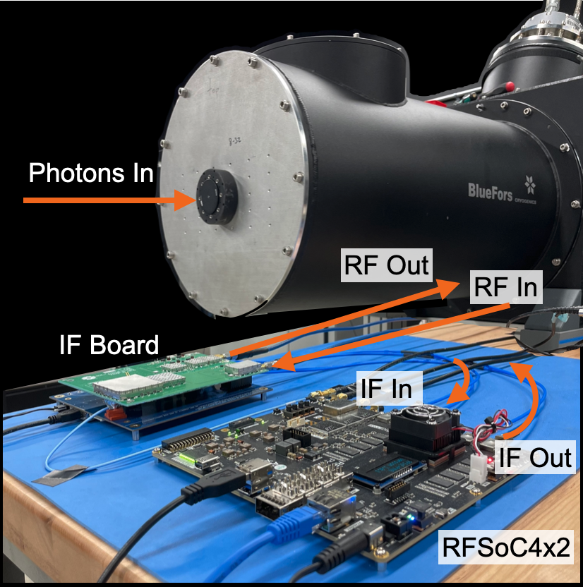
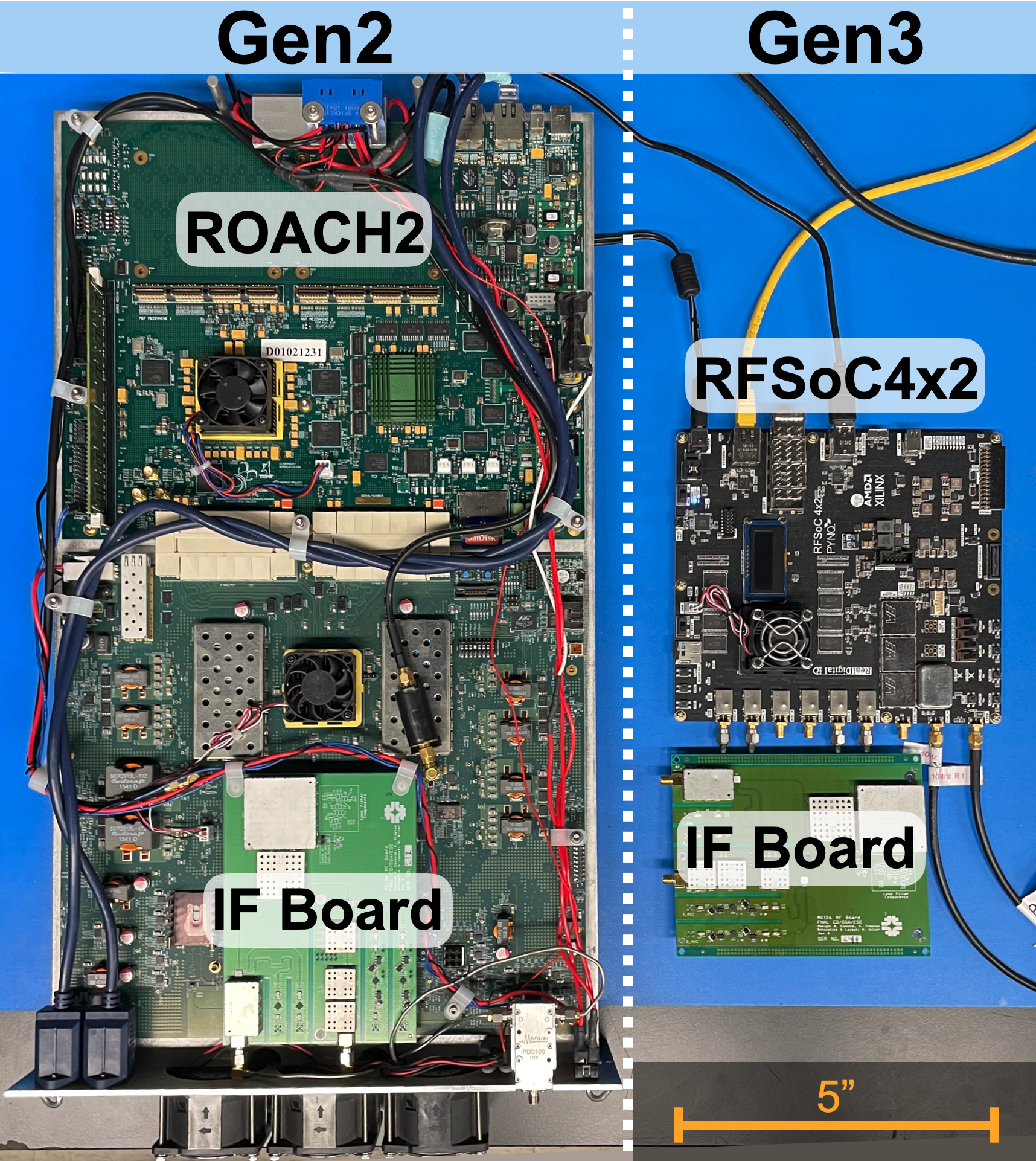
A picture of the Gen3 readout hardware and experimental setup is shown in Fig. 4. Migrating to the RFSoC4x2 platform resulted in a dramatic reduction in the weight, volume, and power of the readout electronics. In addition to using only one fifth the power as the previous Gen2 system, the data converters are twice as fast, allowing us to double the number of detectors read out per board. A to-scale picture showing the size reduction from Gen2 to Gen3 is shown in Fig. 5. Key specifications between the two systems are tabulated in Table 2.
IV.1.1 IF Board and Carrier
The IF board is responsible for translating the 2 GHz readout waveform to the 4-8 GHz microwave band. It is a modified version of the same board used to convert signals in the Gen2 system Fruitwala et al. (2020). To accommodate the RFSoC’s increased bandwidth, we swapped the 630 MHz (LFCN-630+) anti-aliasing filters on the I and Q DAC output IF to RF paths for the 2 GHz version (LFCN-2000+). We also swapped 800 MHz (LFCN-800+) and 1800 MHz (LFCN-1800+) anti-aliasing filters on the I and Q RF to IF ADC input signal paths with the 2 GHz (LFCN-2000+) and 3.8 GHz (LFCN-3800+) versions, respectively.
The input and output RF ports each have two programmable attenuators which together can be adjusted from 0 to 63 dB in steps of 0.25 dB. This allows adjusting the waveform power going into the fridge, to optimally drive the MKID resonators, and into the RFSoC, to utilize the full ADC dynamic range. The IF board receiver path has an amplifier chain totaling 88 dB of gain to boost the small cryogenic signals. The board also features a TRF3765 programmable LO and complex mixers which can be used to sweep RFSoC-driven frequencies to different parts of the microwave readout band.
The IF board is powered by a simple 12 V carrier board (see blue board in Fig. 4 under the IF Board). The programmable components are controlled by the carrier’s Arduino Nano which is commanded by the RFSoC over USB.
IV.1.2 RFSoC4x2
Both RFSoC4x2 DACs and two of the ADCs are run at 4.096 GSPS to create a quadrature sampled readout waveform with frequencies in 2 GHz. The FPGA implements a high-throughput digital signal processing pipeline to down-convert each readout tone and monitor the phase.
The RFSoC integrated ARM core runs Ubuntu-flavored Linux and serves as the command and control hub for each feedline readout. The processing system (PS) and programmable logic (PL) each have 4 GiB of available DDR4 SDRAM. The PL DDR4 serves as a data buffer for setup and calibration captures while the PS DDR4 is used for continuous photon capture and pixel monitoring. All FPGA capture, configuration, and control signals are managed by a Python package running on the PS. The PS is also able to program the IF board LO and attenuators to facilitate sweeps.
The RFSoC4x2 platform has several quirks which impacted system design. The first was data converter synchronization. We found the phase mismatch between the DAC tile clocks disrupted the quadrature phase relation of our signals enough to cause -20 dB image tones. This did not meet our -30 dB IMD requirement (Sec. III) and forced us to implement Multi-Tile Synchronization (MTS)noa (c). MTS suppresses the image tones to -40 dB but adds complexity and constraints to the clocking architecture.
The other quirk was the platform’s default MPSoC clock configuration led the 1 Gigabit Ethernet to perform at roughly one-third capacity. We found the current 4x2 board support package (BSP) configures the full power domain main clock slower than the low power domain switch. We modified the BSP to correct this and recovered near line rate 1 GbE performance. More information on the Zynq UltraScale+ MPSoC is provided in referencenoa (a).
IV.2 FPGA Design
The FPGA design followed a similar strategy to the Gen2 system but with several optimizations to manage double the number of channels and speed up data capture. The MKID readout waveform is computed in software and written to a large FPGA memory buffer where it can be replayed from the DACs in a loop. After the waveform passes through the feedline, it is sampled by the ADCs which feed into an intensive real-time processing pipeline. The digital signal processing steps are described in the following section.
IV.2.1 Digital Signal Processing
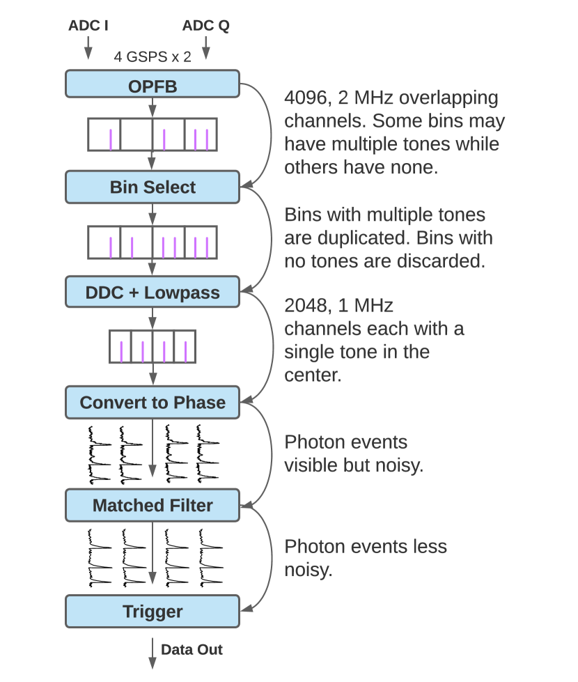
An overview of the key digital signal processing (DSP) steps is shown in Fig. 6. After the 4 GHz waveform is injected into the programmable logic, it must be channelized into 2048 MKID channels. Due to fabrication uncertainties, the channelizer must be able to down-convert 2048 channels from arbitrary position in the microwave band. We use a two-stage oversampled polyphase filter bank (OPFB) channelizer followed by a direct digital-down-converter (DDC). The OPFB produces 4096, 2 MHz coarse channels which overlap 50%. This allows every MKID readout tone to pass through the channelizer un-attenuated. The OPFB was highly-optimized as it is the most resource-intensive step and it is the subject of its own publicationSmith et al. (2021).
After the OPFB, the Bin Select core selects the 2048 user-defined channels which contain MKID readout tones, copying bins with multiple tones as needed, and feeds them to the DDC. The DDC multiplies each channel by the complex conjugate of the readout tone to do the final down-conversion. The DDC core is also responsible for applying each channel’s custom coordinate transform. The DDC complex multiplier includes an optional phase offset which can individually rotate each MKID loop. The core also implements a complex subtraction which serves to center each MKID loop. After each readout tone has been fully down-converted and the coordinate transform has been applied, each channel is low-pass filtered to remove other MKID readout signals that may fall in the same OPFB bin. The channels are decimated to produce 2048, 1 MHz fine channels each with one MKID readout tone in the center.
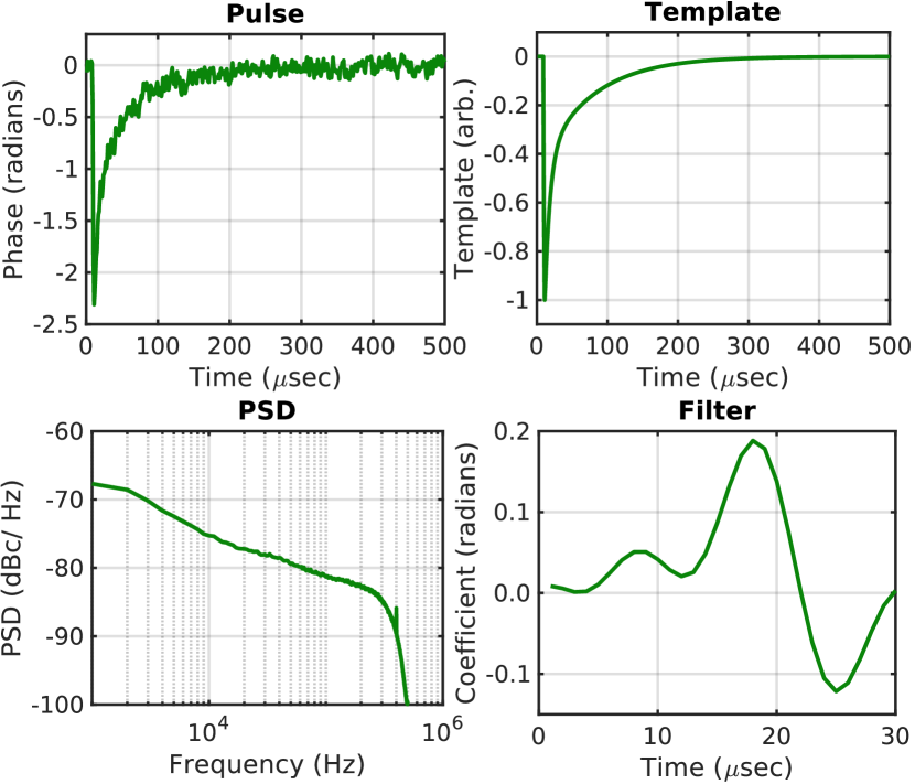
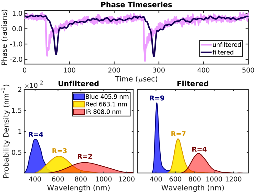
The next step is to convert each channel to phase by evaluating . This operation results in 2048 phase time series each sampled every 1 microsecond. To further reduce phase noise, we apply a custom matched filter to every channel. The matched filter generation process in summarized in Fig. 7. For every pixel on the feedline, we average unfiltered laser photons from the middle of the energy band to characterize the detector signal. We also estimate the channel phase noise by averaging the noise power spectral density when there are no photons arriving. With the measured signal and noise, we construct a matched filter for every channel.
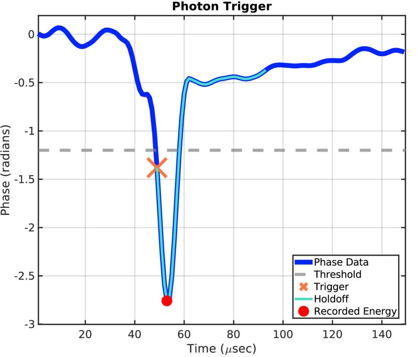
After the matched filter enhances photon signals and suppresses channel-specific noise, we are finally ready for photon triggering. The trigger behavior is shown for a filtered pulse in Fig. 8. Once the pulse crosses the threshold, the channel triggers. The minimum phase value is continually updated for a number of samples specified by the holdoff parameter. After the holdoff counter expires, the photon energy is recorded as the minimum value in the window and the channel is free to trigger again. The photon time, energy, and channel are recorded to disk.
IV.3 Implementation
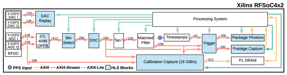
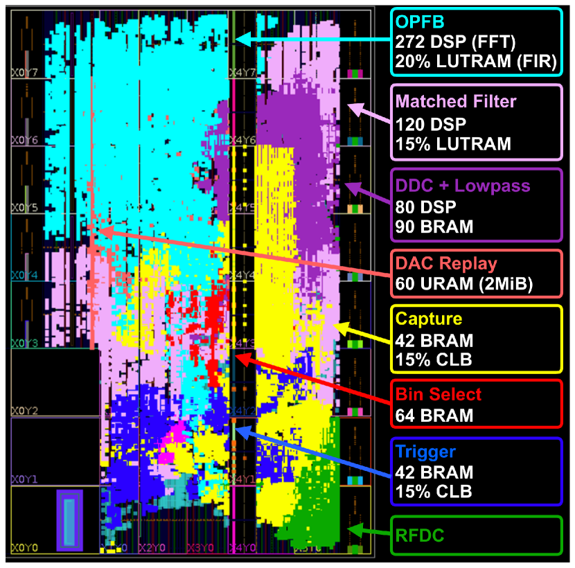
The FPGA design was implemented using Vivado 2021.1 in an IP integrator-based project flow. A system block design is shown in Fig. 9. Resource utilization in summarized in Table 3 and device area utilization is highlighted by block in Fig. 11. The implementation is notable for realizing an intensive signal processing pipeline, requiring a large percentage of the FPGA resources at high clock rates, while using high-level synthesis tools. In this section, we will describe our approach to implementation, starting with our choice of tools.
IV.3.1 Tools
All custom IP blocks, barring a few exceptions discussed below, were implemented using Vitis High-Level Synthesis (HLS) which synthesizes high-level C/C++ code to low-level hardware description language (HDL). HLS has the advantage of being more accessible to scientists without experience in hardware description language (HDL) and can be more flexible and easier to port to new hardware. However, it is notorious for using more resources and increasing timing strain. We developed several strategies for HLS usage to improve resource utilization and timing closure:
-
•
Small, single task, HLS blocks are preferable to complex blocks.
-
•
Clean, small internal functions can significantly improve generated HDL.
-
•
Partitioned temporary variables in unrolled loops is preferable to automatic inference within a loop.
-
•
The ap_ctrl_none pragma directive can significantly improve control and logic optimization.
-
•
Manually picking bits instead of using the DATAPACK pragma directive can be vital.
-
•
It is better to place memory resources such as BRAM and URAM manually using the IP generator in Vivado than to infer them in HLS.
-
•
External AXIS to AXI conversion is necessary for continuous writes.
To help close timing in the full design, we used Vivado Intelligent Design Runs (IDR). IDR uses ML-based strategy predictions and incremental compile to help close timing in Vivado in tight designsnoa (d). We used quality of result (QOR) suggestions and IDR-implemented runs to identify optimizations and achieve timing closure in the full design. Subsystem-specific strategies are discussed in context below.
IV.3.2 Waveform Replay
The DAC Replay block streams a repeating waveform consisting of complex samples from a look-up-table (LUT) to the 4.096 GSPS DACs. The LUT size and DAC sample rate achieve 7.813 kHz frequency resolution for each superimposed tone in the readout comb. The table stores the 32-bit complex samples in a 2 MiB URAM buffer. An external URAM was used in Vivado as opposed HLS inference because HLS would not properly cascade the URAM blocks–a necessary optimization for reducing logic routing resources.
IV.3.3 Channelizer
The OPFB, Bin Select, and DDC subsystems implement the channelizer. The OPFB is implemented using two HLS blocks that route and reorder data, sixteen parallel Xilinx FIR cores that implement the filter, and the Xilinx SSR FFT block exported from System Generator / Model Composer. Full implementation details are provided in Smith et al. (2021).
The Bin Select block caches eight copies of the preceding 4096-point FFT frame and routes them into eight parallel output lanes in any order (i.e., the pathological case of 2048 resonators in a single channel is supported). The channel order is run-time user programmable via AXI4-Lite.
The DDC uses external BRAMs to store phase increments, offsets, and centers which are used with an internal cosine LUT to down-convert the channels and apply the complex rotation and translation coordinate transform. The DDC values are channel-specific and run-time user programmable over AXI4-Lite. A Xilinx FIR filter implements a low-pass and decimate operation to produce the fine channels.
IV.3.4 Convert to Phase and Filter
IV.3.5 Photon Event Trigger
The trigger is user-programmed at run-time with 2048 thresholds and holdoffs unique to each channel. The threshold is encoded as an 8-bit signed value allowing the phase threshold to be set with 0.02 radian precision. The holdoff value indicates the number of samples (microseconds) until a subsequent trigger is permitted. The holdoff takes integer values between 8 and 254. The maximum value of 254 corresponds to 254 microseconds which exceeds the typical filtered pulse recovery time (see Fig. 8).
IV.3.6 Photon Capture
Photon capture is implemented using a pair of 800 KiB buffers. The processing system reads from one buffer while the other records photon data. The buffer is rotated either when full or when two photons arrive a user-defined interval ( s) after the first buffered photon.
IV.3.7 Postage Capture
The postage capture system is capable of recording a 127-microsecond IQ time series window of up to 8000 total trigger events across any of 16 user-selected channels.
IV.3.8 Capture Subsystem
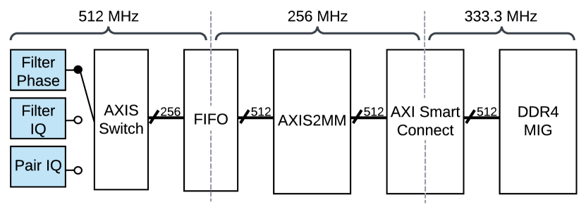
The capture subsystem manages data capture from various places in the signal processing pipeline to facilitate MKID feedline characterization and setup. An overview of the capture hierarchy is shown in Fig. 10. The system is backed by the PL DDR4 which provides 4 GiB of SDRAM storage. It is implemented using parallel HLS blocks that select user-requested groups of channels or, in the case of ADC capture, combine I and Q signals. A small, open-source RTL corenoa (g) is used to translate the AXI4-Stream interface to AXI4 transactions because HLS generated AXI4S-AXI4M interfaces do not support continuous write at the gigabyte level. AXI4 glue logic is used to cross clock domains and buffer the data before it is written to DDR4. The memory interface generator (MIG) is clocked at 333 MHz with a 512-bit bus, providing around >16 GiB/s offload bandwidth.
Routing congestion caused by I/O pins to the PL DDR4 being proximate to the RFDC I/O pins caused trouble closing timing in the capture subsystem. A successful IDR run suggested the problem could be alleviated by constraining the MIG to the right side of the chip to create open lanes for the DAC output routing. The resulting square Pblock is visible in the placement view (see Fig. 11).
IV.3.9 Timestamps
Photon timestamps are provided by a time keeping core that supports several different modes. In basic operation, timestamps are generated using a 19-hour, 1 microsecond counter. All RFSoC boards are synchronized using the pulse-per-second (PPS) input linked to a GPS signal, providing a pulse each time the second rolls over. The current second as determined by UTC accessed from an NTP server by the processing system is synchronized with the PPS signal. The 36-bit, UTC-based timestamp is associated with each phase sample in the trigger block and recorded when a photon event is triggered. The resulting system provides 1 s timing resolution. Absolute timing error between boards was measured to be less than 150 ns888PPS signal was generated by a Stanford Research FS725 10 MHz Rubidium Frequency Standard..
| Resource | Number | % of ZU48DR |
|---|---|---|
| CLB | 36012 | 68% |
| LUT (Logic) | 79809 | 19% |
| LUT (Memory) | 98368 | 46% |
| BRAM999Each BRAM is 36 Kbits. | 262 | 24% |
| URAM | 64 | 80% |
| DSP | 475 | 11% |
IV.4 Software
The project software is based primarily on the Python Productivity for ZYNQ (PYNQ) framework. PYNQ is an open-source, AMD/Xilinx maintained project that facilitates interacting with and programming a ZYNQ architecture-based FPGA through Pythonnoa (h). PYNQ provides a Linux-based image, Jupyter notebook server, and extensible Python packages all running on the MPSoC. The mkidgen3 package includes Python drivers for the FPGA design IP, MKID-specific setup and calibration functions, and diagnostic plots. In the following subsections we detail our adoption and adaptation of the PYNQ framework to support MKID readout.
IV.4.1 Deviations from the PYNQ Image
The mkidgen3 system image has two main modifications from the Ubuntu 22.04-based PYNQ 3.0.1 stock image. First, we reserved a segment in the device tree for the PL DDR4. Editing the device tree allowed more robust, full integration of the PL DDR4 with the PYNQ memory model and recommended pynq.allocate method. The second adaptation was to patch the xrfdc Bare Metal C RFDC driver to include MTS-related functions. These deviations are documented in the main project repository.
IV.4.2 Python Drivers
PYNQ provides a simple methodology to create Python drivers for IP. The framework parses the Vivado-generated hardware hand-off (.hwh) file, effectively auto-discovering IP, and provides the user with a pynq.Overlay object that can be used to command and control design IP through its associated register map. We use this approach to write Python drivers for all configurable IP in the design. The PYNQ drivers can be used directly to set up and read out MKIDs using the on-board Jupyter notebook server or through remote Python execution, i.e., over ssh.
IV.4.3 Server Architecture
The software ecosystem also includes high-level client and server software that facilitate array-level set up, capture, and observations and is intended for use in a multi-board MKID instrument environment. Commands are based on the zmq request-reply pattern with each RFSoC running a feedline server that schedules capture requests from the client and guarantees all captures occur with the required FPGA state. Resulting capture data and status updates are broadcast via the zmq pub-sub pattern, allowing any network device to monitor photon or engineering data. At the time of writing, the server is still undergoing testing and will be fully detailed in a future publication.
V System Performance Characterization
The Gen3 MKID readout system has been successfully demonstrated in lab and meets all performance requirements outlined in Sec. III. The system was characterized in three configurations:
-
1.
RFDC Loopback: The RFSoC4x2 I and Q ADCs are directly connected to the I and Q DACs, respectively, with short, matched cables.
-
2.
IF Loopback: The IF board RF Out is connected to the IF board RF In with a 30 dB fixed attenuator in-between.
-
3.
MKID Measurement: The full system is connected to a cryogenic UVOIR MKID device (see Fig. 12).
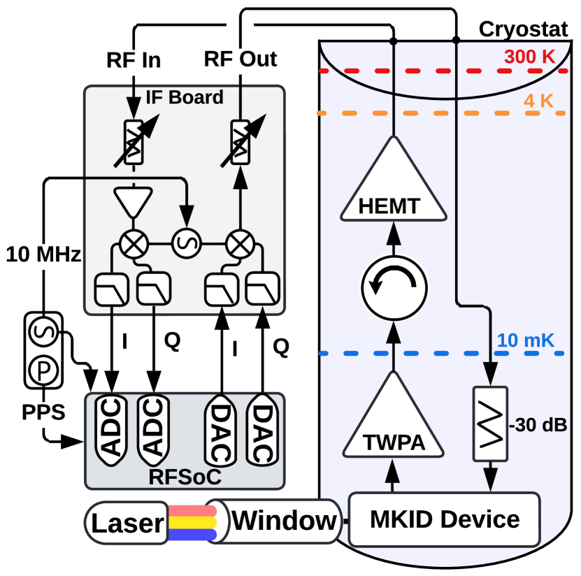
In all configurations, a Stanford Research FS725 10 MHz rubidium frequency standard was used to synchronize the RFSoC4x2 and IF board clocks and provide the PPS signal.
V.1 Multi-MKID Readout Approximation
A pseudo-random comb was used to simulate the simultaneous readout of 2048 MKIDs. The comb consists of a superposition of readout tones where each tone is randomly placed in every other 2 MHz coarse channel in the 2 GHz readout band for a total of 2048 approximately-evenly-spaced tones. The tones are designed to be no closer than 300 kHz to their 2 MHz channel edge which mimics the OPFB overlap region and simplifies channel assignment in the FPGA. The resulting waveform is similar to what we find with modern UVOIR MKID devices and provides realistic conditions for evaluating multi-MKID readout performance.
V.2 Output Comb Performance
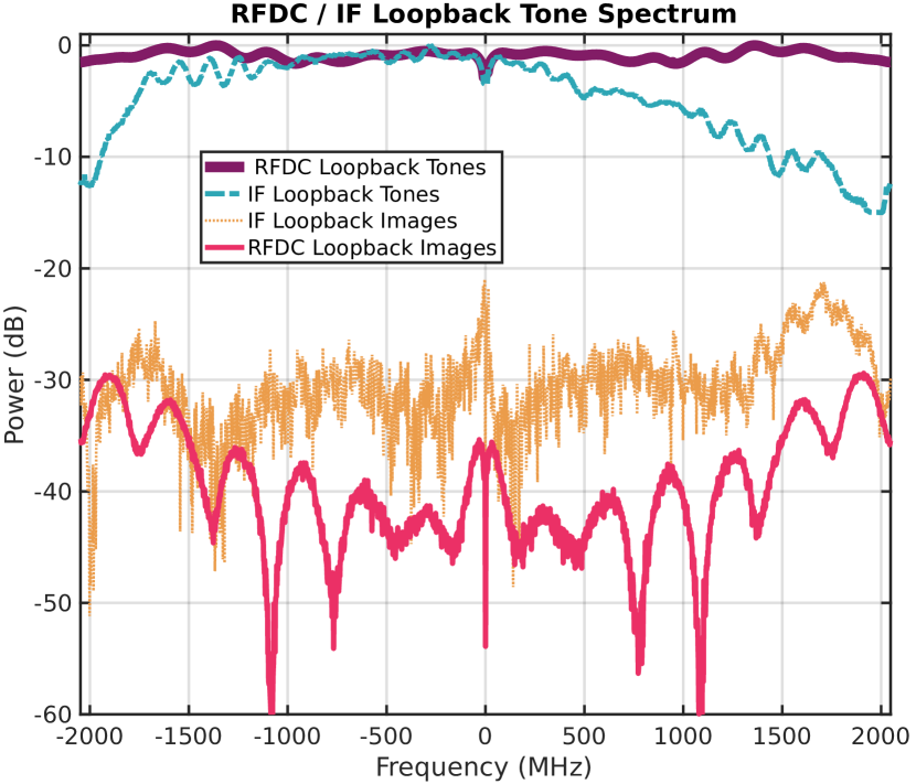
A 2048-tone, uniform-amplitude, pseudo-random-frequency (see Sec.V.1) comb was generated and played out the DACs to simulate an MKID readout waveform. The output tone and image powers for all frequencies in IF loopback and in RFDC loopback are shown in Fig. 13. In RFDC loopback, the comb is fairly uniform, showing only a few dB variation across the 2 GHz readout band. The image tones are at most -30 dB at the band edges and meet our performance requirement (Sec. III.3.2). In the IF loopback, the output tone power is more attenuated and non-uniform across the band. The attenuation at the edges of the 4 GHz band are caused by imperfect roll-off in the IF board analog anti-aliasing low-pass filters (see Sec. IV.1.1). Ripples in the tone power are caused by impedance mismatches which launch reflections and creating standing waves in the IF board. The real-valued frequencies (0, 2 GHz) are more attenuated than the imaginary-valued frequencies (-2 GHz, 0), likely due to excess attenuation in the IF board I signal path. We hypothesize the manual rework of the anti-aliasing filters in-house resulted in poor microwave hygiene and wide variation between signal paths in the IF board, leading to reduced performance.
V.3 Phase Noise
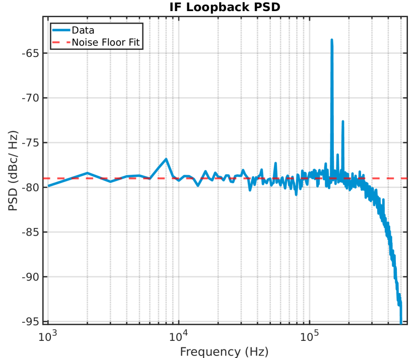
The phase power spectral density from a down-converted readout tone is shown in Fig. 14. The phase noise floor is fit with the red dashed line and is approximately -80 dBc/Hz. There is some line noise present around 150 kHz, possibly from electromagnetic interference in the lab or a nearby image tone. Line noise can also be generated from rounding errors in the DSP pipeline which uses truncation as the default rounding mode to conserve FPGA resources. Truncation can introduce a DC bias, for example in an OPFB channel, which may be up-converted to an image tone during the DDC multiply operation.
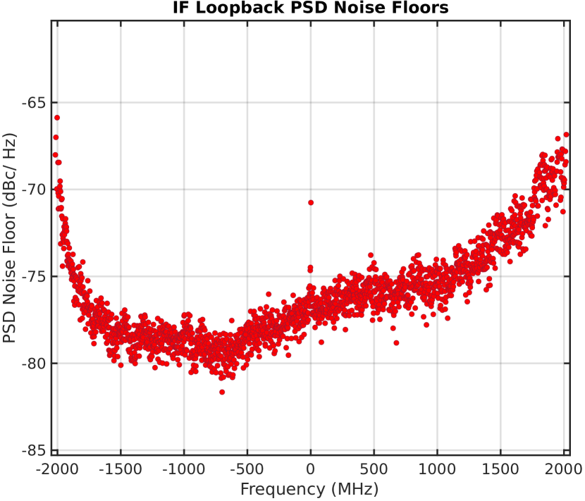
Fig. 15 shows the PSD-floor fit for all 2048 channels in the pseudo-random-tone waveform. The PSD floors follow a pattern inverse to the IF loopback tone power measured in Fig. 13, with the real-valued frequencies showing more noise. This pattern is indicative of the same issue with the IF board microwave hygiene and poor transmission performance in the I signal path.
V.4 MKID Readout
The Gen3 readout system was also characterized in lab using a real MKID and a series of lasers. These studies provide a concrete means to study the system’s energy-resolving capability and help disentangle effects of readout-specific noise on scientific utility.
V.4.1 Experimental Setup
The MKID device was a PtSi-on-sapphire, array-style chip101010Full fabrication details are provided in Szypryt et al. (2017). with the same design and manufacturing process used for the device in MEC and in Zobrist et al. (2019). The MKID was cooled in a dilution refrigerator (20 mK) with a first-stage, quantum-noise-limited parametric amplifierFaramarzi et al. (2024). Lasers at 405.9 nm, 663.1 nm, and 808.0 nm illuminated the MKID through windows in the the dilution refrigerator. The experimental setup is shown in Fig. 12.
A single 4.5 GHz MKID was characterized, biased, and prepared for photon readout using the mkidgen3 Python package on the RFSoC-hosted Jupyter Notebook. The resonator was set up manually using a series of sweeps and was ultimately biased at the correct frequency using the IF board programmable LO, and the correct power using the IF board RF Out programmable attenuator. This technique is not suitable for setting up multiple MKIDs on one feedline because the LO and programmable attenuator provide global frequency and power offsets; however, it provides a decent approximation for the full-setup algorithms and server utility that are currently are under development. To characterize the extra readout noise generated during multi-MKID readout, excess readout tones were pseudo-randomly generated (see Sec. V.1) and propagated through the MKID device and full readout chain.
For maximum flexibility in the data analysis, the raw phase time series was captured with a unity matched filter (no effect) and the matched filter and trigger algorithms were applied in software. The matched filter and trigger performance were verified on the FPGA for a subset of experimental settings.
V.5 Matched Filter Performance
The matched filters are chiefly responsible for boosting the signal-to-noise ratio in the phase time series and improving resolving power. The test MKID’s 30-tap filter was computed as described in Fig. 7 using pulse data from the middle (red, 633.1 nm) laser wavelength. The detector resolving power was characterized with and without the matched filter. In each case, the readout system used a 2048-tone, pseudo-random comb to simulate the noise environment of a full-feedline readout. Results are summarized in Fig. 16 and show a dramatic improvement in resolving power with the matched filter applied.
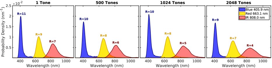
V.6 Resolving Power Results
The detector resolving power, , was measured with different numbers of pseudo-random tones in the readout waveform to characterize the best-case and worst-case scenario performance. Results are summarized in Fig. 17. In the case of only one readout tone in the waveform, we find excellent resolving power that is consistent with Zobrist et al. (2019) and meets our best-case scenario performance requirement (Sec. III.3.3). In the worst-case scenario where we are driving all 2048 tones, we see some degradation in the resolving power but the results are within the acceptable limits set by the Gen2 MEC deployment (Sec. III.3.3).
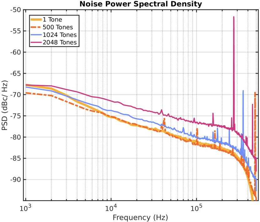
V.7 Resolving Power Degradation with Tone Number
While the resolving power requirements are met, future MKID devices are expected to have better intrinsic resolving power. Understanding the nature of the resolving power degradation is useful for planning system upgrades and drafting requirements for future systems. The MKID phase noise power spectral density for each number of tones is shown in Fig. 18. The data was collected with the readout tone biased to the optimal MKID resonance frequency and power and includes the MKID device two-level system noise as well as noise from the cryogenic amplifier chain. Fig. 18 shows that as the number of tones goes up, both the noise floor and line noise increase.
We hypothesize there are three main ways in which increasing the number of tones in the waveform can raise system noise and decrease resolving power.
-
1.
Reduced DAC Dynamic Range
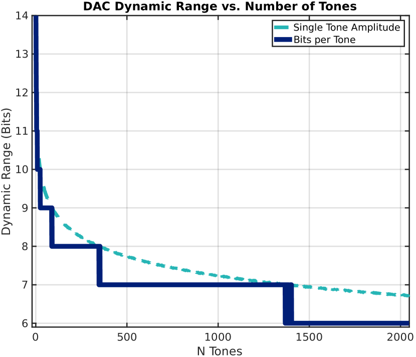
For best noise performance, the DAC maximum voltage output is typically mapped to the maximum value of the readout waveform. The IF board RF Out programmable attenuator can be used to reduce the power level to the optimal MKID drive power (around dBm) as needed. As more tones are added, the maximum value of the superimposed readout waveform grows and there is less available DAC dynamic range per readout tone. The reduction in number of bits available per tone is shown in Fig. 19. This effect increases the quantization noise in each channel.
-
2.
Reduced ADC Dynamic Range
Similar to the DAC, there is also a reduction in ADC dynamic range per tone as more tones are added. Typically, the IF board RF In programmable attenuator is adjusted so the maximum waveform value will be close to the maximum ADC input voltage. The more tones superimposed in the waveform, the fewer bits available per tone. A similar relation to Fig. 19 applies except the RFSoC4x2 ADC maximum dynamic range is 12-bits, not 14.
-
3.
Intermodulation Effects
Finally, there are spurs, intermodulation products, image tones, and reflections all caused by the proliferation of readout tones in the analog domain. These signals may also impact dynamic range in the digital domain, for example, more noise power will cause more signal resolution to be lost during truncation rounding.
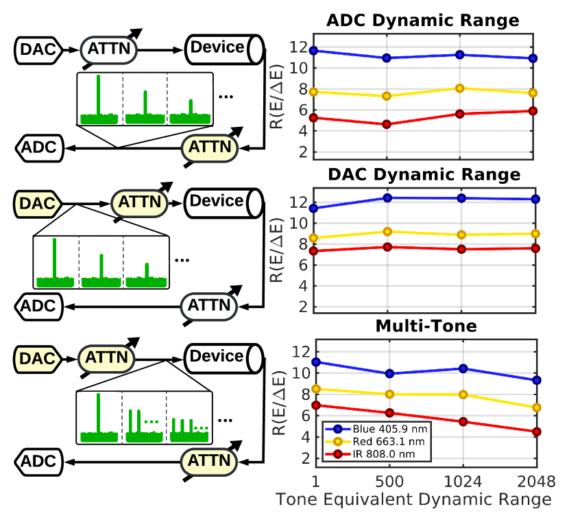
We devised two additional studies to isolate the ADC and DAC dynamic range effects and determine the leading contributor to the resolving power degradation we observe with increasing tone number. In the first study, a single tone was played from the DAC but the waveform was artificially made to use different DAC dynamic ranges in accordance with the values expected for different numbers of tones (see Fig. 19). For each DAC dynamic range setting, the RF Out IF board programmable attenuator was adjusted to ensure the MKID device was still being driven at the correct level. The ADC input attenuator was fixed conservatively at a level consistent with what would be compatible with 2048 tones. In this way, we were able to probe the effects of the loss in DAC dynamic range absent intermodulation products and changes in ADC dynamic range utilization. To study the effects of ADC dynamic range, we again played a single tone from the DAC but this time at a fixed dynamic range, again conservatively in-line with what would be available with 2048 tones. The IF board RF In programmable attenuator was adjusted to purposefully lower the ADC dynamic range used to what would be available per tone for different numbers of tones. Results for these studies is compared with the data collected for the multi-tone experiment in Fig. 20. The experiments show that the degradation in DAC and ADC dynamic range, and consequently the increase in quantization noise, does not significantly impact device resolving power. In all cases, the measured resolving power is similar to what was measured in the best-case scenario with a single tone and maximal ADC/DAC dynamic range utilization. We conclude that spurious tones, intermodulation products, image tones, and reflections caused by the multitude of readout tones is the primary factor driving resolving power degradation with increasing number of tones.
VI Discussion
The Gen3 system characterized in this work is capable of reading out 2048 UVOIR MKIDs across 4 GHz of bandwidth using an RFSoC and IF board. While the system meets all performance requirements outlined in Sec. III and provides a major improvement in UVOIR MKID readout scalability, there are several areas that could be improved and questions that warrant further investigation. Performance-based trade-offs and recommendations are discussed in context below.
VI.1 IF Board IQ Imbalance and Images
We use quadrature sampling in the RFSoC along with IQ mixers in the IF board to access the 4-8 GHz UVOIR MKID band. Quadrature sampling has the benefit of reducing the required data converter speed by half in order to access a given band. At present, this technique is necessary to reach our desired readout band using an RFSoC platform. Unfortunately, quadrature sampling comes at the cost of being very sensitive to gain/phase imbalance between the two quadratures which results in undesired image tones. These imbalances can be corrected at a single frequency but the calibration complexity grows significantly with bandwidth and in practice it is not feasible to calibrate more than about 400 MHz of instantaneous bandwidthnoa (i).
In the RFSoC, using Multi-Tile Synchronizationnoa (c), we achieve enough consistency between the I and Q paths that the image tones are within the -30 dB requirement (Sec. III.3.2); however, this is not the case when the IF board is included (see Fig. 13), with images rising to within -25 dB and even -15 dB in some cases with respect to the driven tones. As discussed in Sec.V.2 and Sec. V.3, the IF board anti-aliasing filters were manually reworked in lab, resulting in poor signal integrity and imbalance between the I and Q paths (see Fig. 13 and Fig. 15). While the current IF board prototype provides a means to measure MKIDs in the lab, it does not meet the performance criteria across the full readout band and is likely not suitable for instrument deployment. With a modest redesign and professional PCB manufacturing, we expect the IF board loopback measurement can achieve 30 dB image tones and uniform -80 dBc / Hz phase noise floor across the band.
VI.2 Direct RF Sampling
Even better than redesigning the IF board would be to do away with it entirely and use a direct RF approach. This eliminates the need for quadrature sampling with separate I and Q signal paths, potentially greatly improving RF signal integrity, readout phase line noise, and ultimately detector resolving power. Current RFSoC devices do not have the data converter speed required to sample 4-8 GHz directly in either the first or second Nyquist zone. It may be possible to use the 5.9 GSPS DFE devicenoa (a) at the maximum rate in the third Nyquist zone but more testing is needed to verify performance. Another approach is to use the second Nyquist zone (2.95-5.9 GHz) and modify the MKID readout band, though this would require significant device re-design and may not be compatible with commercial, low-noise cryogenic amplifiers required to boost the device signal. A faster RFSoC may be available soon in the Versal AI RF part which is advertised as having 36 GHz of analog bandwidth (4 GHz IBW per channel) and would likely be able to directly access the full readout band using the first or second Nyquist zonenoa (j).
With direct-RF-capable platforms on the horizon, the Gen3 system design prioritized platform-upgradability. The modular approach disentangles I/O from core DSP blocks and is backed by a C Makefile and Vivado tcl scripts that that should greatly simplify re-targeting the design to a new RFSoC. The HLS DSP blocks expedite updates by exposing bit-widths, DSP parallelization, and other mutable parameters as top-level C directives. We’ve already seen some success in this approach; we were able to quickly re-target our original ZCU111-based design to the cost-effective, RFSoC4x2 platform shortly after its release. Going forward, these techniques are expected to continue helping us quickly leverage advances in the RFSoC product line.
VI.3 UVOIR MKID Resolving Power
Resolving power is a critical UVOIR MKID capability. As discussed in Sec. III.3.3, the measured resolving power is a conglomeration of many factors and it can be challenging to identify performance requirements that can meaningfully inform design trade-offs. Several recent superconducting detector digital readouts have derived noise requirements from the cryogenic signal chainFruitwala et al. (2020); Yu et al. (2023). Fruitwala et al. (2020) showed the Gen2 UVOIR MKID readout system IF loopback phase noise floor was around -90 dBc/Hz and was lower than the expected phase noise floor contributed by the first-stage, low-noise cryogenic HEMT amplifier ( -85 dBc/Hz)Fruitwala et al. (2020). Here, the measured phase noise floor in the Gen3 system is 5-10 dB higher than this calculated HEMT noise floor (see Fig. 14 and Fig. 15). This is not surprising given Gen3 runs twice as many tones in twice the bandwidth as compared to Gen2. We showed increasing the number of tones raises the system noise in Sec. V.7 and the larger bandwidth is expected to harbor more intermoduation products, reflections, and other spurious signal distortion.
The HEMT phase noise floor is not even the relevant cryogenic amplifier limit in this work because we used a quantum-noise-limited TWPA for the first-stage. Integrating a TWPA before the HEMT lowers the effective cryogenic amplifier noise temperature from around 5 K to close to 0.5 KZobrist et al. (2019), further increasing the gulf between the expected phase noise contributions of the cryogenic signal chain and the Gen3 readout electronics. Despite having higher phase noise than the cryogenic amplifiers, Gen3 achieves respectable resolving power–competitive with dedicated analog electronics in the case of one toneZobrist et al. (2019) and comparable to Gen2 in the case of 2048 tonesWalter et al. (2018).
Our results support the idea that the resolving power is predominately limited by the detector itself. Zobrist et al. (2019) showed the addition of the first stage TWPA in the analog readout system did not improve resolving power as much as the reduction in phase noise would have predicted, indicating a detector limitation. We see a similar pattern in this work where the phase noise in Gen3 is higher than what was achieved in Gen2, yet the resolving power is comparable.
This detector resolving power limitation has been attributed to a variable amount of the incident photon energy escaping into the non-photosensitive detector substrate, leading to a variable detector response. This problem, known in some literature references as “hot phonon escape"Kozorezov et al. (2000, 2007, 2008); de Visser et al. (2021); Zobrist et al. (2022), is not captured in the phase noise power spectral density and is not improved by reduced phase noise in cryogenic or room temperature electronics. Zobrist et al. (2022) fabricated a UVOIR MKID using a bilayer process that reflects energy back into the photosensitive region, recovering at 814 nm. Unfortunately, this bilayer process has not been demonstrated with large, array-style MKID devices and may be impracticable due to difficulties with indium processes. Solving hot phonon escape is an active area of UVOIR MKID design and fabrication research, but for now it presents a fundamental limitation in resolving power.
Our results coupled with previous work suggests UVOIR MKID readout systems should strive to achieve detector-limited resolving power as opposed to holding the phase noise under the contributions of the cryogenic amplifiers. With the addition of quantum-noise-limited TWPAs, this requirement becomes challenging and may come at the cost of increased system complexity and decreased scalability only to have the resolving power limited by the detectors in the end. In this work, we achieve detector-limited resolving power in the best-case scenario with one tone but we see degradation when running all 2048 tones through the readout chain (see Fig. 17). The best-case scenario performance is useful as a tool in lab to characterize devices and inform design and fabrication updates; however, going forward we will strive to achieve detector limited resolving power at scale. Such a solution may require direct RF and or integration of more complex signal processing techniques such as tone trackingYu et al. (2023), a resonator-based coordinate transformZobrist et al. (2021), and a longer matched filter (Fig. 7).
VII Conclusion
In conclusion, we have built a new MKID digital readout based on the RFSoC platform. The system fits twice as many MKID pixels onto a board that can be run with a fifth of the power of the previous system. Gen3 is also less than half the size and a tenth the weight of the Gen2 system. Gen3 utilizes high-level tools which simplify interacting with and programming the FPGA and make it easier for scientists to use, maintain, and upgrade. The system was demonstrated in lab and achieved high-fidelity, detector-limited resolving power in the case of few resonators and showed minimal degradation in with more tones. Experiments showed the degradation is linked to intermodulation products, image tones, and spurs in the analog domain which may be improved with future iterations of the IF board or a switch to a direct RF approach.
Presently, we are continuing to update and improve the digital domain. We plan to adjust the rounding mode to an unbiased algorithm and include intelligent scaling to maximize dynamic range in the programmable logic. We are also working on new algorithms and techniques to expand the taps in the matched filter for improved noise rejection. Overall, we believe this readout system provides a maintainable, scaleable platform to work towards megapixel MKID arrays and future space-based deployment.
Acknowledgements.
We would like to thank our collaborators at Fermilab: Gustavo Cancelo, Leandro Stefanazzi, and Ken Treptow for helping us get started with the RFSoC and for their valuable consultations on digital signal processing approaches. We would also like to thank Ross Martin at Bit by Bit Signal processing for sharing his expertise on high-performance FFTs and for providing us with a power-efficient FFT that will enhance future design flexibility. Lastly, we would like to thank Jack Hickish, Mitch Burnett, and Dan Werthimer along with the rest of the CASPER collaboration for their early advice on FPGA-based signal processing approaches and for providing insight on RFSoC clocking and overall performance.References
- Todaro et al. (2021) S. Todaro, V. Verma, K. McCormick, D. Allcock, R. Mirin, D. Wineland, S. Nam, A. Wilson, D. Leibfried, and D. Slichter, “State Readout of a Trapped Ion Qubit Using a Trap-Integrated Superconducting Photon Detector,” Physical Review Letters 126, 010501 (2021), publisher: American Physical Society.
- Mariantoni et al. (2011) M. Mariantoni, H. Wang, T. Yamamoto, M. Neeley, R. C. Bialczak, Y. Chen, M. Lenander, E. Lucero, A. D. O’Connell, D. Sank, M. Weides, J. Wenner, Y. Yin, J. Zhao, A. N. Korotkov, A. N. Cleland, and J. M. Martinis, “Implementing the Quantum von Neumann Architecture with Superconducting Circuits,” Science 334, 61–65 (2011), publisher: American Association for the Advancement of Science.
- Xia et al. (2021) F. Xia, M. Gevers, A. Fognini, A. T. Mok, B. Li, N. Akbari, I. E. Zadeh, J. Qin-Dregely, and C. Xu, “Short-Wave Infrared Confocal Fluorescence Imaging of Deep Mouse Brain with a Superconducting Nanowire Single-Photon Detector,” ACS Photonics 8, 2800–2810 (2021), publisher: American Chemical Society.
- Niwa et al. (2017) K. Niwa, T. Numata, K. Hattori, and D. Fukuda, “Few-photon color imaging using energy-dispersive superconducting transition-edge sensor spectrometry,” Scientific Reports 7, 45660 (2017), publisher: Nature Publishing Group.
- Zmuidzinas (2012) J. Zmuidzinas, “Superconducting Microresonators: Physics and Applications,” Annual Review of Condensed Matter Physics 3, 169–214 (2012), publisher: Annual Reviews.
- Mazin (2009) B. A. Mazin, “Microwave Kinetic Inductance Detectors: The First Decade,” AIP Conference Proceedings 1185, 135–142 (2009).
- Day et al. (2003) P. K. Day, H. G. LeDuc, B. A. Mazin, A. Vayonakis, and J. Zmuidzinas, “A broadband superconducting detector suitable for use in large arrays,” Nature 425, 817–821 (2003), publisher: Nature Publishing Group.
- Zobrist et al. (2019) N. Zobrist, B. H. Eom, P. Day, B. A. Mazin, S. R. Meeker, B. Bumble, H. G. LeDuc, G. Coiffard, P. Szypryt, N. Fruitwala, I. Lipartito, and C. Bockstiegel, “Wide-band parametric amplifier readout and resolution of optical microwave kinetic inductance detectors,” Applied Physics Letters 115, 042601 (2019).
- Zobrist et al. (2022) N. Zobrist, W. H. Clay, G. Coiffard, M. Daal, N. Swimmer, P. Day, and B. A. Mazin, “Membraneless Phonon Trapping and Resolution Enhancement in Optical Microwave Kinetic Inductance Detectors,” Physical Review Letters 129, 017701 (2022), publisher: American Physical Society.
- Walter et al. (2020) A. B. Walter, N. Fruitwala, S. Steiger, J. I. Bailey, N. Zobrist, N. Swimmer, I. Lipartito, J. P. Smith, S. R. Meeker, C. Bockstiegel, G. Coiffard, R. Dodkins, P. Szypryt, K. K. Davis, M. Daal, B. Bumble, G. Collura, O. Guyon, J. Lozi, S. Vievard, N. Jovanovic, F. Martinache, T. Currie, and B. A. Mazin, “The MKID Exoplanet Camera for Subaru SCExAO,” Publications of the Astronomical Society of the Pacific 132, 125005 (2020), publisher: The Astronomical Society of the Pacific.
- Steiger et al. (2021) S. Steiger, T. Currie, T. D. Brandt, O. Guyon, M. Kuzuhara, J. Chilcote, T. D. Groff, J. Lozi, A. B. Walter, N. Fruitwala, I. John I. Bailey, N. Zobrist, N. Swimmer, I. Lipartito, J. P. Smith, C. Bockstiegel, S. R. Meeker, G. Coiffard, R. Dodkins, P. Szypryt, K. K. Davis, M. Daal, B. Bumble, S. Vievard, A. Sahoo, V. Deo, N. Jovanovic, F. Martinache, G. Doppmann, M. Tamura, N. J. Kasdin, and B. A. Mazin, “SCExAO/MEC and CHARIS Discovery of a Low-mass, 6 au Separation Companion to HIP 109427 Using Stochastic Speckle Discrimination and High-contrast Spectroscopy*,” The Astronomical Journal 162, 44 (2021), publisher: The American Astronomical Society.
- Swimmer et al. (2022) N. Swimmer, T. Currie, S. Steiger, G. M. Brandt, T. D. Brandt, O. Guyon, M. Kuzuhara, J. Chilcote, T. Tobin, T. D. Groff, J. Lozi, J. I. I. Bailey, A. B. Walter, N. Fruitwala, N. Zobrist, J. P. Smith, G. Coiffard, R. Dodkins, K. K. Davis, M. Daal, B. Bumble, S. Vievard, N. Skaf, V. Deo, N. Jovanovic, F. Martinache, M. Tamura, N. J. Kasdin, and B. A. Mazin, “SCExAO and Keck Direct Imaging Discovery of a Low-mass Companion Around the Accelerating F5 Star HIP 5319*,” The Astronomical Journal 164, 152 (2022), publisher: The American Astronomical Society.
- Iii et al. (2022) J. I. B. Iii, B. A. Mazin, J. P. Smith, C. S. Kim, W. H. Clay, N. Zobrist, N. J. Swimmer, S. Steiger, and M. Daal, “M-MOST: The MKID Multi-Object Echelle(tte) Spectrographic Testbench,” in Advances in Optical and Mechanical Technologies for Telescopes and Instrumentation V, Vol. 12188 (SPIE, 2022) p. 121884Z.
- Fruitwala et al. (2020) N. Fruitwala, P. Strader, G. Cancelo, T. Zmuda, K. Treptow, N. Wilcer, C. Stoughton, A. B. Walter, N. Zobrist, G. Collura, I. Lipartito, J. I. Bailey, and B. A. Mazin, “Second generation readout for large format photon counting microwave kinetic inductance detectors,” Review of Scientific Instruments 91, 124705 (2020), publisher: American Institute of Physics.
- Note (1) https://github.com/MazinLab/MKIDGen3.
- Gao (2008) J. Gao, The Physics of Superconducting Microwave Resonators, Ph.D. thesis, California Institute of Technology (2008).
- Mazin (2005) B. A. Mazin, Microwave Kinetic Inductance Detectors, Ph.D. thesis, California Institute of Technology (2005).
- Zobrist (2022) N. Zobrist, Improving the Resolving Power of Ultraviolet to NearInfrared Microwave Kinetic Inductance Detectors, PhD Thesis, University of California, Santa Barbara, Santa Barbara, CA (2022).
- Szypryt et al. (2016) P. Szypryt, B. A. Mazin, G. Ulbricht, B. Bumble, S. R. Meeker, C. Bockstiegel, and A. B. Walter, “High quality factor platinum silicide microwave kinetic inductance detectors,” Applied Physics Letters 109, 151102 (2016).
- Coiffard et al. (2020) G. Coiffard, M. Daal, N. Zobrist, N. Swimmer, S. Steiger, B. Bumble, and B. A. Mazin, “Characterization of sputtered hafnium thin films for high quality factor microwave kinetic inductance detectors,” Superconductor Science and Technology 33, 07LT02 (2020), publisher: IOP Publishing.
- Mazin (2020) B. A. Mazin, “Superconducting Materials for Microwave Kinetic Inductance Detectors,” (2020), arXiv:2004.14576 [astro-ph, physics:cond-mat].
- Szypryt et al. (2017) P. Szypryt, S. R. Meeker, G. Coiffard, N. Fruitwala, B. Bumble, G. Ulbricht, A. B. Walter, M. Daal, C. Bockstiegel, G. Collura, N. Zobrist, I. Lipartito, and B. A. Mazin, “Large-format platinum silicide microwave kinetic inductance detectors for optical to near-IR astronomy,” Optics Express 25, 25894–25909 (2017), publisher: Optica Publishing Group.
- Zobrist et al. (2021) N. Zobrist, N. Klimovich, B. Eom, G. Coiffard, M. Daal, N. J. Swimmer, S. Steiger, B. Bumble, H. G. LeDuc, P. K. Day, and B. A. Mazin, “Improving the dynamic range of single photon counting kinetic inductance detectors,” Journal of Astronomical Telescopes, Instruments, and Systems 7, 010501 (2021), publisher: SPIE.
- Note (2) We set our requirement at 808 nm despite the fact MEC was characterized at 850 nm due to difference in availability of laser sources between Subaru Telescope and our lab at UCSB.
- Strader et al. (2013) M. J. Strader, M. D. Johnson, B. A. Mazin, G. V. S. Jaeger, C. R. Gwinn, S. R. Meeker, P. Szypryt, J. C. v. Eyken, D. Marsden, K. O’Brien, A. B. Walter, G. Ulbricht, C. Stoughton, and B. Bumble, “EXCESS OPTICAL ENHANCEMENT OBSERVED WITH ARCONS FOR EARLY CRAB GIANT PULSES,” The Astrophysical Journal Letters 779, L12 (2013), publisher: The American Astronomical Society.
- Guo et al. (2023) S. Guo, J. Tan, H. Zhang, J. Wang, T. Ji, L. Zhang, X. Hu, J. Chen, J. Xie, K. Zou, Y. Meng, X. Bei, L.-A. Wu, Q. Chen, H. Wang, X. Tu, X. Jia, Q.-Y. Zhao, L. Kang, and P. Wu, “High-timing-precision detection of single X-ray photons by superconducting nanowires,” National Science Review 11, nwad102 (2023).
- noa (a) “Zynq UltraScale+ RFSoC ZCU670 Evaluation Kit,” (a).
- noa (b) “RF-ADC Multi-Band Operation • Zynq UltraScale+ RFSoC RF Data Converter v2.6 Gen 1/2/3/DFE LogiCORE IP Product Guide (PG269) • Reader • AMD Technical Information Portal,” (b).
- (29) John I. Bailey III, Jennifer P. Smith, Benjamin A. Mazin, Gustavo I. Cancelo, Leandro Stefanazzi, Aled Cuda, Nicholas Zobrist, and Kenneth Treptow, “MKIDGen3: a scalable readout for next-generation kilopixel UVOIR MKIDs,” (SPIE, Yokohama, Japan).
- noa (c) “Multi-Tile Synchronization • Zynq UltraScale+ RFSoC RF Data Converter v2.6 Gen 1/2/3/DFE LogiCORE IP Product Guide (PG269) • Reader • AMD Technical Information Portal,” (c).
- Smith et al. (2021) J. P. Smith, J. I. Bailey, J. Tuthill, L. Stefanazzi, G. Cancelo, K. Treptow, and B. A. Mazin, “A High-Throughput Oversampled Polyphase Filter Bank Using Vivado HLS and PYNQ on a RFSoC,” IEEE Open Journal of Circuits and Systems 2, 241–252 (2021), conference Name: IEEE Open Journal of Circuits and Systems.
- noa (d) “Intelligent Design Runs • Vivado Design Suite User Guide: Design Analysis and Closure Techniques (UG906) • Reader • AMD Technical Information Portal,” (d).
- noa (e) “CORDIC,” (e).
- noa (f) “FIR Compiler,” (f).
- noa (g) “MazinLab/wb2axip: Bus bridges and other odds and ends,” (g).
- Note (3) PPS signal was generated by a Stanford Research FS725 10 MHz Rubidium Frequency Standard.
- noa (h) “PYNQ,” (h).
- Note (4) Full fabrication details are provided in Szypryt et al. (2017).
- Faramarzi et al. (2024) F. Faramarzi, R. Stephenson, S. Sypkens, B. H. Eom, H. LeDuc, and P. Day, “A 4-8 GHz Kinetic Inductance Travelling-Wave Parametric Amplifier Using Four-Wave Mixing with Near Quantum-Limit Noise Performance,” (2024), arXiv:2402.11751 [astro-ph, physics:quant-ph].
- noa (i) “Image Due to IQ Imbalance • Co-location Deployment Considerations for Direct RF Sampling Transceivers (WP541) • Reader • AMD Technical Information Portal,” (i).
- noa (j) “Aerospace and Defense Platforms,” (j).
- Yu et al. (2023) C. Yu, Z. Ahmed, J. C. Frisch, S. W. Henderson, M. Silva-Feaver, K. Arnold, D. Brown, J. Connors, A. J. Cukierman, J. M. D’Ewart, B. J. Dober, J. E. Dusatko, G. Haller, R. Herbst, G. C. Hilton, J. Hubmayr, K. D. Irwin, C.-L. Kuo, J. A. B. Mates, L. Ruckman, J. Ullom, L. Vale, D. D. Van Winkle, J. Vasquez, and E. Young, “SLAC microresonator RF (SMuRF) electronics: A tone-tracking readout system for superconducting microwave resonator arrays,” Review of Scientific Instruments 94, 014712 (2023).
- Walter et al. (2018) A. Walter, B. Mazin, C. Bockstiegel, N. Fruitwala, P. Szypryt, I. Lipartito, S. Meeker, N. Zobrist, G. Collura, G. Coiffard, P. Strader, O. Guyon, J. Lozi, and N. Jovanovic, “MEC: the MKID exoplanet camera for high contrast astronomy at Subaru (Conference Presentation),” (2018) p. 31.
- Kozorezov et al. (2000) A. G. Kozorezov, A. F. Volkov, J. K. Wigmore, A. Peacock, A. Poelaert, and R. den Hartog, “Quasiparticle-phonon downconversion in nonequilibrium superconductors,” Physical Review B 61, 11807–11819 (2000), publisher: American Physical Society.
- Kozorezov et al. (2007) A. G. Kozorezov, J. K. Wigmore, D. Martin, P. Verhoeve, and A. Peacock, “Electron energy down-conversion in thin superconducting films,” Physical Review B 75, 094513 (2007), publisher: American Physical Society.
- Kozorezov et al. (2008) A. G. Kozorezov, J. K. Wigmore, D. Martin, P. Verhoeve, and A. Peacock, “Phonon Noise in Thin Metal Films in an Advanced Energy Down-Conversion Stage,” Journal of Low Temperature Physics 151, 51–57 (2008).
- de Visser et al. (2021) P. J. de Visser, S. A. de Rooij, V. Murugesan, D. J. Thoen, and J. J. Baselmans, “Phonon-Trapping-Enhanced Energy Resolution in Superconducting Single-Photon Detectors,” Physical Review Applied 16, 034051 (2021), publisher: American Physical Society.