Visualizing the microscopic origins of topology in twisted molybdenum ditelluride
In moiré materials with flat electronic bands and suitable quantum geometry, strong correlations can give rise to novel topological states of matter Sharpe2019 ; Serlin2020 ; Cai2023 ; Park2023 ; Zeng2023 ; Fan2023 ; Foutty2023 ; Kang2024 ; Lu2024 . The nontrivial band topology of twisted molybdenum ditelluride (tMoTe2) — responsible for its fractional quantum anomalous Hall (FQAH) states Cai2023 ; Park2023 ; Zeng2023 ; Fan2023 — is predicted to arise from a layer-pseudospin skyrmion lattice Wu2018_topological ; yu_giant_2020 . Tracing the layer polarization of wavefunctions within the moiré unit cell can thus offer crucial insights into the band topology. Here, we use scanning tunneling microscopy and spectroscopy (STM/S) to probe the layer-pseudospin skyrmion textures of tMoTe2. We do this by simultaneously visualizing the moiré lattice structure and the spatial localization of its electronic states. We find that the wavefunctions associated with the topological flat bands exhibit a spatially-dependent layer polarization within the moiré unit cell. This is in excellent agreement with our theoretical modeling Zhang_Polarization_2023 , thereby revealing a direct microscopic connection between the structural properties of tMoTe2 and its band topology. Our work enables new pathways for engineering FQAH states with strain, as well as future STM studies of the intertwined correlated and topological states arising in gate-tunable devices.
Moiré bilayers of semiconducting transition metal dichalcogenides (TMDs) have rapidly emerged as rich platforms for studying novel strongly correlated phases of matter Wang2020 ; waters_flat_2020 ; Regan2020 ; Zhang2020 ; Li2021 ; Ghiotto2021 ; Huang2021 ; Anderson2023 ; Cai2023 ; Park2023 ; Zeng2023 ; Fan2023 ; Kang2024 ; Foutty2023 ; Li2021_2 ; Li2024 . Strikingly, the topological properties of these correlated states are remarkably sensitive to the precise atomic structure and materials composition of the moiré lattice. At a doping of one hole per moiré unit cell, correlated insulators can have associated Chern numbers of either 0 or 1 depending on the specific TMDs (e.g., WSe2 vs. MoTe2) and the precise twist angle, , used to construct the moiré lattice Wang2020 ; Cai2023 ; Park2023 ; Zeng2023 ; Fan2023 ; Kang2024 ; Foutty2023 . Furthermore, the long-sought FQAH states have so far only been seen in tMoTe2 over a relatively narrow range of twist angles Cai2023 ; Park2023 ; Zeng2023 ; Fan2023 , and have not been observed in analogous twisted WSe2 structures. It is therefore critical to develop a more comprehensive understanding of the origin and nature of the nontrivial topology in these materials.
The variability of these topological properties can be traced down to microscopic origins Zhang_Polarization_2023 , particularly the textures of electric polarization arising within the TMD homobilayer moiré unit cell. These generate a spatially-varying layer polarization of the flat-band wavefunction described by a layer-pseudospin skyrmion lattice. Charges hopping in this pseudospin skyrmion lattice acquire a geometric phase equivalent to the effect of a real-space magnetic field, giving rise to nontrivial band topology Wu2018_topological ; yu_giant_2020 . The locations of the north and south poles of the skyrmion lattice, where the flat-band wavefunctions become fully layer polarized, are determined by two competing mechanisms: out-of-plane ferroelectric dipole moments resulting from the broken inversion symmetry of the local stacking Wang2022 ; Molino2023 ; Zhang2023_plasmons , and strain-induced in-plane piezoelectric charges resulting from atomic relaxations in the moiré lattice Duerloo2012 ; McGilly2020 ; shaffique2023 ; mao_lattice_2023 . As the structural properties of the moiré lattice are tuned by parameters such as twist angle and strain, these two polarization terms can conspire to flip the location of the north and south poles of the skyrmion lattice between different atomic stacking sites within the moiré unit cell, thereby changing the Chern numbers of the bands Zhang_Polarization_2023 .
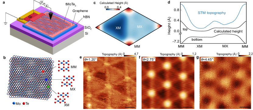
Here, we probe the microscopic origins of topology in tMoTe2 by mapping the spatial localization of valence band wavefunctions as a function of energy using scanning tunneling microscopy and spectroscopy. We fabricate high-quality van der Waals (vdW) devices consisting of tMoTe2 atop monolayer graphene and hexagonal boron nitride (hBN) (Fig. 1a, Extended Data Fig. 1 and Methods), in which the graphene acts only as a local drain electrode for tunneling electrons Zhang2015 ; pan_quantum-confined_2018 ; Zhang2020 ; tilak_moire_2023 ; Molino2023 . We use several spectroscopy methods to distinguish valence band states originating from the K and points of the monolayer MoTe2 Brillouin zone. By studying the local density of states (LDOS) within the moiré unit cell as a function of energy, we find that the topological bands from the K points localize around only certain high-symmetry atomic stacking sites, whereas the trivial states from the point localize at all positions within the moiré unit cell. Our observations of sub-moiré localization of the LDOS in the flat bands are consistent with the layer-pseudospin skyrmion textures predicted by our density functional theory (DFT) calculations.
Twist-angle–dependent lattice relaxations
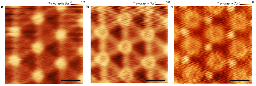
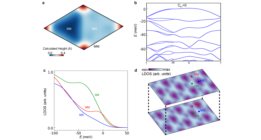
We first examine the moiré lattice structure of tMoTe2 at various twist angles. When two MoTe2 monolayers are twisted atop one another, three high-symmetry stacking sites can be identified based on the relative arrangement of the metal (molybdenum) and chalcogen (tellurium) atoms: MM, in which metal atoms sit atop each other; MX, in which a metal atom sits atop a chalcogen atom; and XM, in which a chalcogen atom sits atop a metal atom (Fig. 1b). Atomic relaxation effects, including in-plane strain and out-of-plane buckling, result in different heights of the top MoTe2 layer at each of these three stacking sites. These effects are captured by our DFT simulations, as shown in Fig. 1c for . The black curves in Fig. 1d show the calculated heights of both MoTe2 layers, plotted along a cut across the moiré unit cell. The MX and XM stacking registries are related by symmetry (rotation by 180∘ around the axis connecting nearest-neighbor MM sites).
These predictions allow us to determine the corresponding high-symmetry stacking sites in our STM topographs. Figures 1e-g show topography images of tMoTe2 with twist angles of , , and , respectively. The blue curve in Fig. 1d shows the measured height of the sample along the same cut through the moiré lattice as for the black curves. The topographic measurement is performed using a large tip bias, typically over V away from the bias of the valence band edge, such that the effects of the spatially varying LDOS are minimized (see Extended Data Fig. 2 for topographs acquired with different tunneling parameters). We find that our measurement is qualitatively consistent with the calculation, allowing us to assign the highest topography point to the MM stacking site, the second highest to MX, and the lowest to XM.
These topographs further reveal the substantial effects of lattice relaxations in tMoTe2. These effects play only a subtle role at , for which the MM, MX, and XM regions account for roughly comparable areas within the moiré unit cell. However, relaxation effects are easily visible at , with the area of the MM regions shrinking relative to the triangular MX and XM domains, along with the formation of solitonic domain walls connecting the MM sites. Relaxation effects are especially profound at , in which there are very large triangular MX and XM domains and comparatively small regions of MM stacking. The obvious effects of relaxations even at twist angles approaching are a consequence of the relative softness of the MoTe2 membrane (as compared to much stiffer materials such as graphene) shaffique2023 . Notably, large lattice relaxations play a key role in determining the topology of the flat bands in theoretical modeling Zhang_Polarization_2023 . Understanding their microscopic properties is thus crucial for learning more about the nature of the observed FQAH states.
Spectroscopic fingerprints of tMoTe2
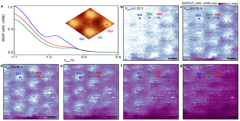
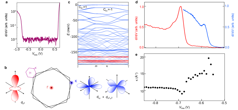
We now turn our attention to the key spectroscopic features of tMoTe2. Fig. 2a shows a representative differential conductance (d/d) spectrum obtained over a large range of sample bias, . The broad region of very small differential conductance surrounding corresponds to the semiconducting band gap of tMoTe2. Although careful measurements reveal the valence band edge to be at V, the onset of large differential conductance in Fig. 2a instead appears at V. This discrepancy stems from the high variation of the tunneling decay constant, , within the tMoTe2 valence band, which effectively conceals the valence band edge in conventional constant-height d/d spectroscopy (see Methods for further discussion).
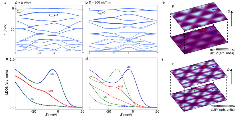
States at the valence band edge originate from the K point of the monolayer MoTe2 Brillouin zone Zhang2015 ; Zhang2020 ; Zhao2020 , and therefore have a large decay constant in tunneling experiments owing to a large crystal momentum mismatch between the K point and the -wave of an ideal STM tip. An additional contribution to their large decay constant comes from the phase mismatch between the -wave of the tip and the dxy+d orbital character of the K-point states in MoTe2 monolayer_Liu2013 , as sketched in Fig. 2b. In a twisted MoTe2 bilayer, the electronic bands of each monolayer hybridize and are folded into a smaller moiré Brillouin zone (as depicted by the purple hexagon in Fig. 2b). As a consequence, the highest energy moiré valence bands share a similarly large decay constant. Fig. 2c shows a DFT calculation of the resulting band structure for tMoTe2 with , with bands colored in blue (red) arising from the K () point of the monolayer MoTe2 Brillouin zone. The first few valence bands originating from the K point are relatively flat and isolated, and carry non-zero valley Chern numbers, , where K and K’ represent the locked valley and spin degrees of freedom. States originating from the point are well separated from these K-point bands, first emerging at an energy of meV below the edge of the valence band.
In order to acquire d/d spectra of the moiré flat band states with adequate resolution, we perform a modified version of the conventional constant-height spectroscopy. We first stabilize the tip at a fixed height above the sample, then turn off the feedback loop and move the tip towards the sample by a fixed distance (typically between nm), and finally sweep while measuring d/d. We refer to this technique as “reduced-height spectroscopy” (see Methods for additional details). The blue curve in Fig. 2d shows a representative spectrum acquired in this way. The bump at V corresponds to the first few flat bands of tMoTe2, all smeared into a single feature. The red curve in Fig. 2d shows a conventional constant-height d/d spectrum acquired from the same area of the sample. In this measurement, d/d is almost immeasurably small over the range of in which we see the K-band states with reduced-height spectroscopy. Instead, we see a large d/d peak at V that arises from bands which originate from the point of the monolayer MoTe2 Brillouin zone. These states have small crystal momentum and primarily out-of-plane character Zhao2020 , and thus result in a large d/d signal compared with K-point states.
We verify the origin of these features by measuring as a function of bias (see Fig. 2e and Methods). We observe a dip in coincident with the large d/d peak seen in the red curve in Fig. 2d. This dip is consistent with the prediction that these states primarily arise from bands originating from the point. Additionally, the increased decay constant for V confirms the K-point origin of the valence band edge. The offset between K- and -point states is consistent with the calculation, in which bands from are first found at an energy of meV below the top of the moiré valence band.
Spatial localization of valence band wavefunctions
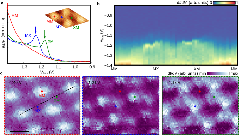
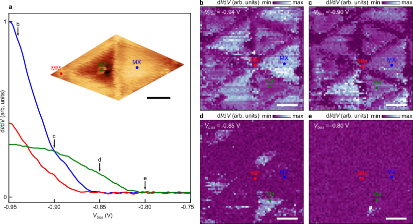
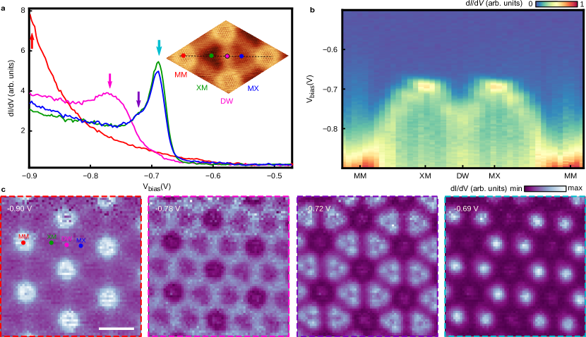
Fig. 3a shows four representative d/d spectra taken at different positions within the moiré unit cell. These spectra are acquired with standard constant-height spectroscopy, such that observed features originate primarily from -point moiré bands. The green and blue curves are taken at the XM and MX stacking sites, the red at MM, and the pink at the center of a solitonic domain wall (DW) connecting MM sites. We see that these d/d spectra exhibit considerable spatial variation within the moiré unit cell. Fig. 3b shows a line-cut of d/d spectra obtained along the dashed black line in the inset of Fig. 3a. From this map, we see a large d/d peak that is at its lowest energy at the MX and XM sites, and smoothly drifts to its largest energy at the MM sites.
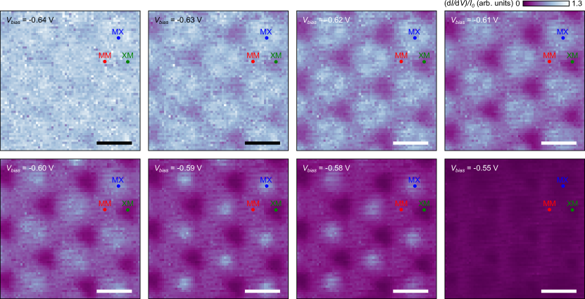
The spatial variation of the -point states can be best seen in maps of d/d acquired at fixed (Fig. 3c), which provide a direct visualization of the wavefunction distribution within the moiré unit cell and its energy dependence. Consistent with the spectra in Figs. 3a-b, we see that d/d at V is largest at the MM sites, then shifts to the domain walls as the bias is lowered to V, further develops into a more complex geometry at V that is not localized on any high-symmetry stacking site, and finally localizes onto the MX and XM sites at V. Collectively, these measurements show that the -point wavefunctions can reside at any position within the moiré unit cell, with the details depending sensitively on energy. The precise localization of these states is highly dependent on the exact combination of twist angle, heterostrain, and interlayer separation (see Supplementary Information). Similar behavior was observed over a wide range of twist angles, shown in Extended Data Fig. 3 for 3.52∘ and Extended Data Fig. 4 for 1.20°.
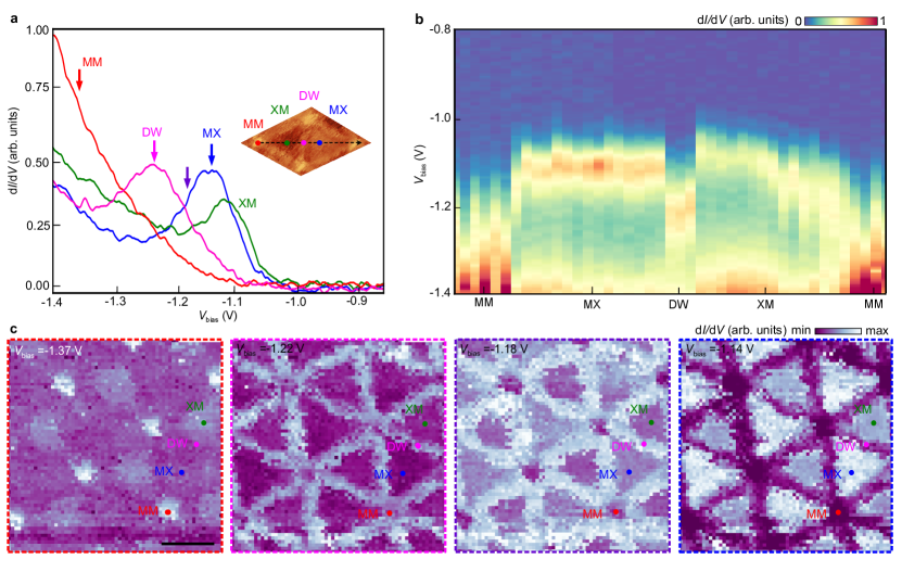
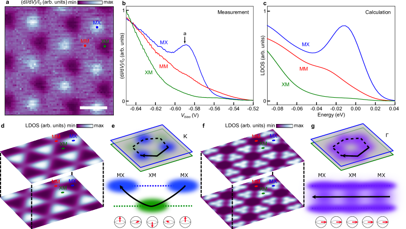
In sharp contrast, we find that the flat-band states originating from the K points only reside at certain positions within the moiré unit cell. Fig. 4a shows a representative reduced-height d/d spectroscopy map acquired with V (additional maps are shown in Extended Data Fig. 5 and Supplementary Video 2). The map is normalized by the initial current of the spectrum, , in order to mitigate artifacts inherent to the reduced-height spectroscopy technique (see Supplementary Information for a discussion of this normalization, and Supplementary Information Fig. S2 for the raw d/d spectra). The normalized d/d is largest at the MX stacking site, and becomes progressively weaker at MM and XM. Fig. 4b shows the reduced-height spectroscopy spanning a small range of at these three stacking sites. We see that the d/d peak previously identified in Fig. 2d exists only on the MX stacking site, and that d/d is largest at MX over nearly the entire range of shown (see Supplementary Information for a discussion of the hierarchy of (dd)/ at V). A replication of this behavior at is shown in Extended Data Fig. 6, and its evolution in the small- limit is shown in Extended Data Fig. 7.
Layer-pseudospin textures and band topology
The particular spatial localization of the flat bands we observe is well captured by our machine-learning assisted large-scale DFT calculations. Fig. 4c shows the calculated LDOS at MX, XM, and MM in the top MoTe2 layer over the same range of energy as in Fig. 4b. The calculation is in excellent qualitative agreement with our experimental observations, in particular showing the largest LDOS at MX over the entire range of energy shown. Fig. 4d further shows a spatial map of the calculated LDOS for both the top and bottom layers of the twisted MoTe2 (corresponding to an energy of meV in Fig. 4c). Since tunneling from the STM tip is primarily sensitive to the top layer of tMoTe2, we directly compare our (dd)/ map in Fig. 4a with the calculation for the top MoTe2 layer shown in Fig. 4d. The calculated LDOS is largest around the MX sites in the top MoTe2 layer, consistent with our experimental observation of largest d/d at MX.
The layer-dependent localization of the flat-band wavefunctions to different high-symmetry stacking sites in the moiré unit cell is the key feature responsible for generating nontrivial band topology. The local layer polarization can be mapped onto a pseudospin Bloch sphere, in which the top (bottom) of the sphere corresponds to a wavefunction polarized to the top (bottom) MoTe2 layer. Under this mapping, the MX site is the north pole and the XM site the south pole. As the electron hops inside the moiré unit cell, the trajectory of the layer pseudospin will cover the entire Bloch sphere, giving rise to winding number of 1 (illustrated schematically in Fig. 4e) hasan_colloquium_2010 . This skyrmion lattice generates a pseudo-magnetic field responsible for the anomalous Hall effect seen in transport experiments yu_giant_2020 , analogous to the topological Hall effect driven by skyrmions of electron spin found in certain magnetic materials nagaosa_topological_2013 .
The layer-polarizion of the flat-band wavefunctions contrasts that of the -point states, which can appear at any position within the moiré unit cell (Fig. 3c). This is anticipated theoretically, since these -point states are strongly interlayer-hybridized and are thus unable to polarize to a single MoTe2 sheet. Fig. 4f shows a calculation of the LDOS at an energy of meV below the valence band edge, comparable to the d/d map acquired at V in Fig. 3c. The experiment and theory agree very well, in that both show wavefunction localization nearly equivalently onto the MX and XM sites in both layers (see Supplementary Information for a discussion of weak symmetry-breaking terms). For these interlayer-hybridized bonding states, the layer pseudospin is pinned to a narrow region on the equator of the Bloch sphere and the resulting texture is topologically trivial (illustrated schematically in Fig. 4g, with the direction along the equator chosen arbitrarily).
A potential complication in interpreting our measurements lies in understanding the effect of a local electric field under the STM tip, arising from the large and an intrinsic work function mismatch between the tip and the sample. We have performed additional DFT calculations similar to those described above, but also including a realistic tip-induced external electric field (see Methods and Extended Data Fig. 8). We find that the states originating from the point have an almost negligible dependence on the external field owing to their interlayer hybridization. In contrast, the relative weight of the K-point states shifts towards one of the two MoTe2 layers, depending on the sign of the external field. Nevertheless, the geometry of the LDOS localization within the moiré unit cell remains unchanged. Thus, a tip-induced field does not meaningfully impact the primary conclusions of our analysis.
Discussion and outlook
Our STM/S study of tMoTe2 provides the first microscopic visualization of this unique topological material. Accurately predicting the Chern numbers and quantum geometry of the flat valence bands has been challenging owing to their extreme sensitivity to the modeling parameters Wu2018_topological ; Zhang_Polarization_2023 ; Wang2024 ; jia_moire_2023 ; ahn_first_2024 . Our detailed energy-dependent LDOS maps and atomically-resolved topographs now provide strong experimental constraints for theory. In particular, our observation of MX-localized wavefunctions in the top MoTe2 layer is in excellent agreement with our modeling. Our theory further reveals that the in-plane atomic lattice relaxations within the moiré lattice are instrumental in controlling the topological properties of the material. In calculations with in-plane lattice relaxations artificially excluded, the north and south poles of the pseudospin lattice flip positions between MX and XM and also change the Chern numbers of the flat bands (Extended Data Fig. 9). This new understanding unveils the intimate connection between the precise atomic lattice structure of tMoTe2 and its quantum geometric properties.
Looking forward, the structure of the LDOS within the moiré unit cell and its evolution with energy can now be used to further refine theories beyond simply predicting the correct Chern number. This will help to provide sharper constraints on the FQAH effect in tMoTe2, likely resulting in a better understanding of experimentally observed states and aiding predictions for entirely new phases. Our results also provide insights into the atomic-scale electric polarization structure of tMoTe2 arising from the combination of microscopic ferroelectric and piezoelectric contributions, informing ongoing studies of the moiré ferroelectricity found in twisted TMD bilayers Zhang_Polarization_2023 ; McGilly2020 ; Wang2022 ; Molino2023 ; Zhang2023_plasmons and opening new pathways towards engineering the FQAH states with strain Liu2024_strain . Lastly, our foundational atomic-scale understanding of the system enables future STM/S experiments probing the intertwined correlated and topological states that emerge upon hole doping. Progress in this direction will require the development of new device geometries with Ohmic contacts to the tMoTe2, obviating the need for a graphene substrate and enabling gating to the integer and fractional Chern insulator states.
Methods
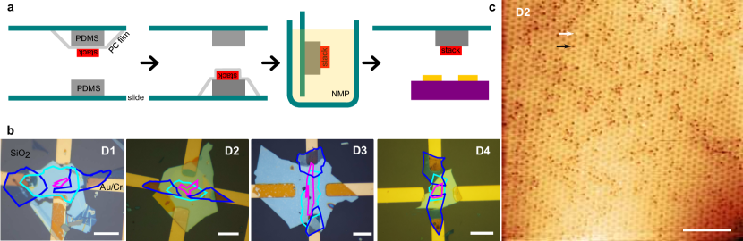
Device fabrication. Our vdW hetereostructures are fabricated using a standard dry transfer technique with a poly(bisphenol A carbonate) (PC) film on a polydimethylsiloxane (PDMS) puck. Flakes of graphite, hBN, and 2H-MoTe2 are exfoliated onto a SiO2/Si wafer and are then picked up using the PC stamp in the following order: hBN, monolayer graphene, tMoTe2, graphite. The graphite covers only a portion of the graphene, and extends beyond the hBN to eventually establish electrical connection to the STM wiring. To assemble the tMoTe2, we first identify two adjacent monolayer MoTe2 flakes (which likely have the same orientation of their crystal axes), or cut a single monolayer MoTe2 flake in half using a sharp metal tip affixed to a micromanipulator. We then pick up the two pieces of MoTe2 sequentially, rotating the sample stage by the desired twist angle after picking up the first piece. After the entire vdW heterostructure is assembled, the PC film is peeled off the PDMS puck by hand, and carefully placed upside-down onto a different PDMS puck. At this point, the tMoTe2 is in direct contact with the PDMS, and the entire vdW stack is covered by PC. The PC film is then dissolved using N-Methyl-2-pyrrolidone (NMP) and subsequently washed with isopropyl alcohol (IPA), leaving just the vdW stack resting on PDMS.
In parallel, a SiO2/Si substrate is pre-patterned with evaporated metal electrodes. These electrodes are fabricated using standard optical lithography and electron-beam metal evaporation (5 nm of Cr followed by 50 nm of Au) techniques. The wafer is attached to the STM sample plate using silver epoxy, and wires are hand-pasted between the evaporated Cr/Au electrodes and the electrical contacts on the STM sample plate. Next, the vdW stack is deposited directly onto the Cr/Au electrodes by pressing down the PDMS puck onto the substrate. The graphite contacts are oriented such that they land on the pre-patterned Cr/Au electrodes, taking care not to unintentionally short electrodes together. The vdW stack delaminates easily from the PDMS, and as a result it is flipped upside down from its original assembly such that the tMoTe2 is furthest from the substrate and remains exposed for STM measurements. Lastly, any residual PDMS contamination is removed from the surface of the tMoTe2 by densely scanning with an atomic force microscope (AFM) tip operated in contact mode. Our technique is illustrated in Extended Data Fig. 1a, and is a modified version of that first introduced in Ref. Choi2019 . Extended Data Fig. 1b shows optical images of the final devices used in this study. The MoTe2 flakes for device D1 are from homegrown crystals grown using Te flux, those for device D2, D3, and D4 are from commercial crystals from HQ Graphene. The data for the region is from device D1, and all other data is from devices D2, D3, and D4.
Because MoTe2 degrades when exposed to air, all vdW device assembly steps involving MoTe2 are performed in an argon environment in a glovebox (0.1 ppm O2 and H2O). The completed device is transferred directly from the glovebox into the STM load lock chamber using a vacuum transfer suitcase. This process results in clean MoTe2 surface that is almost entirely free of residue. Fig. 1c shows a representative STM topograph of a 100 nm by 100 nm region of a tMoTe2 sample, showing that atomic defects in the MoTe2 are the primary form of disorder in our samples (rather than sample degradation).
Effects of the graphene substrate. We use a graphene substrate in our devices owing to challenges in otherwise forming Ohmic contact to tMoTe2 at cryogenic temperatures. We find that monolayer graphene efficiently collects electrons tunneled into the tMoTe2. Because of the large mismatch in the atomic lattice constants of graphene and MoTe2, states at the K points of each material are separated by a large crystal momentum and do not strongly hybridize. We estimate the size of the Fermi pocket around the K point in tMoTe2 from the calculated dispersion of untwisted bilayer MoTe2. Similarly, we estimate the size of the Fermi pocket in graphene by assuming a linear dispersion, , with m/s wallace_band_1947 . We find that at energies up to 1 eV below the valence band edge of tMoTe2, and with no interlayer twist, the Fermi pockets of MoTe2 and graphene are separated by at least 2 nm-1 and thus do not hybridize. Twisting the two materials further separates the low-energy states. Therefore, we expect that the primary effects of the graphene substrate compared to a standard dielectric (such as hBN) are: (i) creating an isopotential surface for the bottom MoTe2 layer, and (ii) weakly modifying the precise form of the tMoTe2 lattice relaxations (see Supplementary Information for additional discussion). Lastly, at a practical level, the graphene substrate also precludes gating experiments since it partially screens the electric field effect from the silicon back gate.
STM/STS measurements. Our measurements are performed using a Scienta Omicron Polar STM in an ultrahigh vacuum cryogenic environment with base temperature of K. The sample plate has ten isolated electrical contacts, enabling the use of either scanning gate microscopy or capacitive searching andrei_capa techniques to navigate to the small tMoTe2 sample. In our experimental setup, the tMoTe2 sample is grounded and a voltage bias is applied to the tip. To facilitate the interpretation of our d/d spectra, we plot the data in terms of sample bias, which is related to the tip bias as follows: . The STM tip is made by electrochemically etching a tungsten wire. The end of the STM tip is shaped on the evaporated gold electrode nearby the tMoTe2 by pulsing and poking into the gold until the STM scanning is reliable and the curve exhibits a perfectly linear slope.
The d/d spectra are acquired using a phase-sensitive detection with a mV peak-to-peak AC voltage modulation at a frequency of either 317 Hz or 419 Hz. The first harmonic of the demodulated signal is proportional to d/d and thus to the local density of states. The energy resolution for spectroscopy is meV where the first term corresponds to the thermal broadening and the second accounts for the instrumental broadening from the lock-in modulation. Note that this broadening is underestimated because the transmission of tunneling quasiparticles grows exponentially with bias, so that at larger bias there is a high number of tunneling channels that make d/d sensitive to the LDOS over a broader range of energy lang_spectroscopy_1986 .
We use either conventional constant-height spectroscopy or a modified “reduced-height” spectroscopy technique to probe electronic states, depending on the relative magnitude of their decay constant. In particular, larger is observed for states originating from -point bands due both to the in-plane orbital character of these states monolayer_Liu2013 and to their higher crystal momentum , following equation TersoffHamann ; TosattiChen . Here, is the average work function of the tip and the sample, is the bias and the energy of the tunneling electrons involved.
To perform constant-height spectroscopy, the tip is first stabilized at a given current and bias setpoint, . Then the feedback loop is turned off and is swept across the range of interest while measuring dd. Such measurements can be acquired over a spatially resolved grid of points, generating a series of LDOS maps with high energy resolution, high tip stability, and minimal tip-induced doping (since the tip is kept relatively far the sample at all times). These grid spectroscopy measurements are analyzed using STMaPy (Scanning Tunneling Microscopy analysis in Python), a data analysis tool written in Python stmapy . We use this technique mainly to study bands originating from the point.
When performing reduced-height spectroscopy, the spectra are acquired in the same way, however the tip is moved closer to the sample by a fixed distance, , before is swept. This allows for stabilization far away from the sample, avoiding artifacts stemming from position-dependent height variations and tip-sample interactions that arise when the tip is stabilized closer to the sample (see Supplementary Information). The pre-measurement height reduction serves to enhance the d/d signal from states with larger originating from the K points. Because small fluctuations in the stabilization condition can be exponentially amplified at a decreased tip-sample separation, we normalize individual spectra by the initial current, , to make comparisons across spectra more consistent (see Supplementary Information for a discussion on the normalization).
Decay constant measurements. Decay constant measurements are performed by fitting measurements of at different . For each bias voltage, the tip is first stabilized at a current setpoint of 10 pA and then gradually retracted by a distance of 1 nm while the tunneling current is measured. curves are fit using , where is the tip-sample separation and is the decay constant.
Determination of intrinsic heterostrain in the experiment. All topography images acquired by STM are analysed using Gwyddion and Inkscape. Following the procedure described in Refs. Artaud2016 ; huder_electronic_2018 , the relative strain between the MoTe2 layers is determined in the most general case by solving the following equation relating the top layer atomic lattice, , and the bottom layer atomic lattice, , as determined from atomically resolved images:
| (1) |
In this scheme, starting with the bottom lattice which is assumed to be undeformed, a biaxial deformation quantified by is first applied, then the lattice is rotated by , after which a uniaxial deformation quantified by is applied in the original direction, and finally the lattice is further rotated by , yielding the top lattice. The twist angle is thus , and the uniaxial strain is applied in the direction with respect to the moiré wavevector.
For STM images without atomic resolution, we follow reference Kerelski2019 in assuming Poisson behaviour of the lattice and minimize the following equation using the moiré lengths as input parameters:
| (2) |
with the MoTe2 Poisson ratio estimated to be Duerloo2012 , and the anisotropic heterostrain oriented in the direction with respect to the moiré lattice vectors. This method is used for the regions from Fig. 1e, Extended Data Fig. 4, and Extended Data Fig. 7. In this case, we are sensitive to piezo calibration artifacts and overlook biaxial heterostrain. The latter has been consistently found to be non-negligible in other regions of the sample, and is therefore the main source of error in the determination of the twist angle, which is likely overestimated here by a fraction of a degree.
DFT calculations. We use neural network (NN) potentials to perform lattice relaxations of moiré superlattices. The NN potentials are parameterized using the deep potential molecular dynamics (DPMD) method zhang2018deep ; wang2018deepmd . To generate training datasets, we perform 5000-step ab initio molecular dynamics (AIMD) simulations for tMoTe2 at K using the vasp package kresse1996efficiency , with van der Waals corrections considered within the D2 formalism grimme2006semiempirical . More details on parameterizing NN potentials can be found in Ref. Zhang_Polarization_2023 . Subsequently, the trained NN potentials are employed to relax the moiré superlattice using the lammps package thompson2022lammps until the maximum atomic force is less than 10-4 eV/Å.
The moiré band structures and LDOS are calculated using the siesta package soler2002siesta , with the inclusion of spin-orbit coupling. We employ the optimized norm-conserving Vanderbilt (ONCV) pseudopotential hamann2013optimized , the Perdew-Burke-Ernzerhof (PBE) functional perdew1996generalized , and a double-zeta plus polarization basis. To sample the moiré Brillouin zone for LDOS calculations, a -grid of is utilized, where is the wavevector. The real-space distribution of the wavefunction is approximated by the weight of projected wavefunction onto the Mo and Te atomic orbitals. Gaussian smearing with a width of 33 meV is applied to smooth the LDOS curves for comparison to experimental data. For the calculated LDOS curves corresponding to specific stacking sites, we average LDOS values within a circle of radius 10 Å for MX, XM, and MM.
Effects of a tip-induced electric field on the K- and -point wavefunctions. The large work function mismatch between gold (which coats the end of the tungsten STM tip) and MoTe2 workfunction-Aftab ; workfunction-Mleczko creates a substantial electric field between the tip and grounded graphene. This, in conjunction with the applied tip bias, can create an electric field under the tip that locally dopes the tMoTe2 and deforms the moiré bands. Previous studies of tMoTe2 have shown that an electric field can modify the nature of the correlated states Cai2023 ; Park2023 ; Zeng2023 ; Fan2023 . Extended Data Figs. 8a-b show zoom-ins of the moiré band structure near the band edge for both and . Although the band structure features several Chern bands, the presence of a finite electric displacement field, , causes band inversions and splittings that result in topologically trivial bands.
To investigate the dependence of the LDOS structure on , we calculate the LDOS at different high symmetry points in both MoTe2 layers for both zero and finite as shown in Extended Data Fig. 8c-d (solid curves correspond to the top layer, and dashed to the bottom). The main consequence of a finite is an energy splitting between the peak at MX in the top layer and the peak at XM in the bottom layer, indicating a slight layer polarization. The calculated LDOS spatial maps in Extended Data Fig. 8e further illustrate that induces some degree of layer polarization. Despite this, we see that the system retains the overall geometry of LDOS localization at MX in the top layer, as seen at in Fig. 4d. Although finite can modify the Chern number of the bands to zero, the LDOS geometry we observe is nevertheless indicative of flat bands that can have a finite Chern number at . In contrast, spatial maps of the LDOS at the point at finite , shown in Extended Data Fig. 8f, are nearly indistinguishable from those at due to strong interlayer hybridization. In summary, the LDOS localization we see provides detailed information to compare with band structure calculations predicting the topology of the bands, though the experimental data does not uniquely indicate the Chern number.
Acknowledgements
We thank D. Waters and B. LeRoy for valuable technical discussions. Experimental and theoretical research on the topological properties of twisted molybdenum ditelluride is supported as part of Programmable Quantum Materials, an Energy Frontier Research Center funded by the U.S. Department of Energy (DOE), Office of Science, Basic Energy Sciences (BES), under award DE-SC0019443. The development of twisted molybdenum ditelluride samples and their basic STM characterization is supported by the U.S. Department of Energy, Office of Science, Office of Basic Energy Sciences under Award Number DE-SC0023062. X.X. and M.Y. acknowledge support from the State of Washington-funded Clean Energy Institute. E.T. was supported by grant no. NSF GRFP DGE-2140004. This work made use of shared fabrication facilities provided by NSF MRSEC 1719797. Machine learning and first-principles calculations are in-part supported by the discovering AI@UW Initiative and AI-Core of the Molecular Engineering Materials Center at the University of Washington (DMR-2308979). This work was facilitated through the use of advanced computational, storage, and networking infrastructure provided by the Hyak supercomputer system and funded by DMR-2308979. K.W. and T.T. acknowledge support from the Elemental Strategy Initiative conducted by the MEXT, Japan (grant no. JPMXP0112101001) and JSPS KAKENHI (grant nos. 19H05790, 20H00354 and 21H05233).
Author contributions. E.T., K.T.C., and F.M. fabricated the devices and performed the measurements. X.-W.Z. performed the DFT calculations under the supervision of T.C. and D.X. C.H., Y.Z., J.Y., and J.-H.C. grew some of the MoTe2 crystals used in this study. K.W. and T.T. grew the BN crystals. H.P., J.C., E.A., and X.X. provided valuable discussion on device fabrication and data interpretation. M.Y. supervised the project. E.T., K.T.C., F.M., and M.Y. wrote the paper with input from all authors.
Competing interests
The authors declare no competing interests.
Additional Information
Correspondence and requests for materials should be addressed to Ting Cao, Di Xiao or Matthew Yankowitz.
Data Availability
Source data are available for this paper. All other data that support the findings of this study are available from the corresponding author upon request.
References
- (1) Sharpe, A. L. et al. Emergent ferromagnetism near three-quarters filling in twisted bilayer graphene. Science 365, 605–608 (2019).
- (2) Serlin, M. et al. Intrinsic quantized anomalous Hall effect in a moiré heterostructure. Science 367, 900–903 (2020).
- (3) Cai, J. et al. Signatures of fractional quantum anomalous Hall states in twisted MoTe2. Nature 622, 63–68 (2023).
- (4) Park, H. et al. Observation of fractionally quantized anomalous Hall effect. Nature 622, 74–79 (2023).
- (5) Zeng, Y. et al. Thermodynamic evidence of fractional Chern insulator in moiré MoTe2. Nature 622, 69–73 (2023).
- (6) Xu, F. et al. Observation of integer and fractional quantum anomalous hall effects in twisted bilayer . Phys. Rev. X 13, 031037 (2023).
- (7) Foutty, B. A. et al. Mapping twist-tuned multi-band topology in bilayer WSe2. Science 384, 343–347 (2024).
- (8) Kang, K. et al. Evidence of the fractional quantum spin Hall effect in moiré MoTe2. Nature 628, 522–526 (2024).
- (9) Lu, Z. et al. Fractional quantum anomalous Hall effect in multilayer graphene. Nature 626, 759–764 (2024).
- (10) Wu, F., Lovorn, T., Tutuc, E., Martin, I. & MacDonald, A. H. Topological insulators in twisted transition metal dichalcogenide homobilayers. Phys. Rev. Lett. 122, 086402 (2019).
- (11) Yu, H., Chen, M. & Yao, W. Giant magnetic field from moiré induced Berry phase in homobilayer semiconductors. National Science Review 7, 12–20 (2020).
- (12) Zhang, X.-W. et al. Polarization-driven band topology evolution in twisted MoTe2 and WSe2. Nature Communications 15, 4223 (2024).
- (13) Wang, L. et al. Correlated electronic phases in twisted bilayer transition metal dichalcogenides. Nature Materials 19, 861–866 (2020).
- (14) Waters, D. et al. Flat Bands and Mechanical Deformation Effects in the Moiré Superlattice of MoS2-WSe2 Heterobilayers. ACS Nano 14, 7564–7573 (2020).
- (15) Regan, E. C. et al. Mott and generalized Wigner crystal states in WSe2/WS2 moiré superlattices. Nature 579, 359–363 (2020).
- (16) Zhang, Z. et al. Flat bands in twisted bilayer transition metal dichalcogenides. Nature Physics 16, 1093–1096 (2020).
- (17) Li, H. et al. Imaging moiré flat bands in three-dimensional reconstructed WSe2/WS2 superlattices. Nature Materials 20, 945–950 (2021).
- (18) Ghiotto, A. et al. Quantum criticality in twisted transition metal dichalcogenides. Nature 597, 345–349 (2021).
- (19) Huang, X. et al. Correlated insulating states at fractional fillings of the WS2/WSe2 moiré lattice. Nature Physics 17, 715–719 (2021).
- (20) Anderson, E. et al. Programming correlated magnetic states via gate controlled moiré geometry. Science 381, 325–330 (2023).
- (21) Li, H. et al. Imaging two-dimensional generalized Wigner crystals. Nature 597, 650–654 (2021).
- (22) Li, H. et al. Mapping charge excitations in generalized Wigner crystals. Nature Nanotechnology (2024).
- (23) Wang, X. et al. Interfacial ferroelectricity in rhombohedral-stacked bilayer transition metal dichalcogenides. Nature Nanotechnology 17, 367–371 (2022).
- (24) Molino, L. et al. Ferroelectric Switching at Symmetry-Broken Interfaces by Local Control of Dislocations Networks. Advanced Materials 35 (2023).
- (25) Zhang, S. et al. Visualizing moiré ferroelectricity via plasmons and nano-photocurrent in graphene/twisted-WSe2 structures. Nature Communications 14, 6200 (2023).
- (26) Duerloo, K.-A. N., Ong, M. T. & Reed, E. J. Intrinsic piezoelectricity in two-dimensional materials. The Journal of Physical Chemistry Letters 3, 2871–2876 (2012).
- (27) McGilly, L. J. et al. Visualization of moiré superlattices. Nature Nanotechnology 15, 580–584 (2020).
- (28) Mohammed, M. A. E., Gayani, N. P. & Shaffique, A. Analytical model for atomic relaxation in twisted moiré materials (2023). ArXiv:2401.00498.
- (29) Mao, N. et al. Lattice relaxation, electronic structure and continuum model for twisted bilayer MoTe$_2$ (2023). ArXiv:2311.07533 [cond-mat].
- (30) Zhang, C. et al. Probing critical point energies of transition metal dichalcogenides: surprising indirect gap of single layer WSe2. Nano Letters 15, 6494–6500 (2015).
- (31) Pan, Y. et al. Quantum-confined electronic states arising from moiré pattern of MoS2-WSe2 heterobilayers. Nano Letters 18, 1849–1855 (2018).
- (32) Tilak, N., Li, G., Taniguchi, T., Watanabe, K. & Andrei, E. Y. Moiré potential, lattice relaxation, and layer polarization in marginally twisted MoS2 bilayers. Nano Letters 23, 73–81 (2023).
- (33) Zhao, W. et al. Direct measurement of the electronic structure and band gap nature of atomic-layer-thick 2H-MoTe2 (2020). ArXiv:2001.05894.
- (34) Liu, G.-B., Shan, W.-Y., Yao, Y., Yao, W. & Xiao, D. Three-band tight-binding model for monolayers of group-vib transition metal dichalcogenides. Phys. Rev. B 88, 085433 (2013).
- (35) Hasan, M. Z. & Kane, C. L. Colloquium : Topological insulators. Reviews of Modern Physics 82, 3045–3067 (2010).
- (36) Nagaosa, N. & Tokura, Y. Topological properties and dynamics of magnetic skyrmions. Nature Nanotechnology 8, 899–911 (2013).
- (37) Wang, C. et al. Fractional Chern Insulator in Twisted Bilayer . Phys. Rev. Lett. 132, 036501 (2024).
- (38) Jia, Y. et al. Moiré fractional chern insulators I: first-principles calculations and continuum models of twisted bilayer MoTe2. Phys. Rev. B 109, 205121 (2024).
- (39) Ahn, C.-E., Lee, W., Yananose, K., Kim, Y. & Cho, G. Y. First Landau level physics in second moiré band of twisted bilayer MoTe2 (2024). ArXiv:2403.19155 [cond-mat].
- (40) Liu, Z. et al. Continuously tunable uniaxial strain control of van der Waals heterostructure devices (2024). ArXiv:2404.00905 [cond-mat].
- (41) Choi, Y. et al. Electronic correlations in twisted bilayer graphene near the magic angle. Nature Physics 15, 1174 (2019).
- (42) Wallace, P. R. The band theory of graphite. Physical Review 71, 622–634 (1947). URL https://link.aps.org/doi/10.1103/PhysRev.71.622.
- (43) Li, G., Luican, A. & Andrei, E. Y. Self-navigation of a scanning tunneling microscope tip toward a micron-sized graphene sample. Review of Scientific Instruments 82, 073701 (2011).
- (44) Lang, N. D. Spectroscopy of single atoms in the scanning tunneling microscope. Physical Review B 34, 5947–5950 (1986). URL https://link.aps.org/doi/10.1103/PhysRevB.34.5947. Publisher: American Physical Society.
- (45) Tersoff, J. & Hamann, D. R. Theory of the scanning tunneling microscope. Phys. Rev. B 31, 805–813 (1985).
- (46) Selloni, A., Carnevali, P., Tosatti, E. & Chen, C. D. Voltage-dependent scanning-tunneling microscopy of a crystal surface: Graphite. Phys. Rev. B 31, 2602–2605 (1985).
- (47) Huder, L., Mesple, F. & Renard, V. T. #scanning tunneling microscopy analysis in python (2023). URL https://doi.org/10.5281/zenodo.7991365.
- (48) Artaud, A. et al. Universal classification of twisted, strained and sheared graphene moiré superlattices. Scientific Reports 6, 25670 (2016).
- (49) Huder, L. et al. Electronic Spectrum of Twisted Graphene Layers under Heterostrain. Physical Review Letters 120, 156405 (2018). URL https://link.aps.org/doi/10.1103/PhysRevLett.120.156405.
- (50) Kerelsky, A. et al. Maximized electron interactions at the magic angle in twisted bilayer graphene. Nature 572, 95–100 (2019).
- (51) Zhang, L., Han, J., Wang, H., Car, R. & Weinan, E. Deep potential molecular dynamics: a scalable model with the accuracy of quantum mechanics. Physical review letters 120, 143001 (2018).
- (52) Wang, H., Zhang, L., Han, J. & Weinan, E. Deepmd-kit: A deep learning package for many-body potential energy representation and molecular dynamics. Computer Physics Communications 228, 178–184 (2018).
- (53) Kresse, G. & Furthmüller, J. Efficiency of ab-initio total energy calculations for metals and semiconductors using a plane-wave basis set. Computational materials science 6, 15–50 (1996).
- (54) Grimme, S. Semiempirical gga-type density functional constructed with a long-range dispersion correction. Journal of computational chemistry 27, 1787–1799 (2006).
- (55) Thompson, A. P. et al. Lammps-a flexible simulation tool for particle-based materials modeling at the atomic, meso, and continuum scales. Computer Physics Communications 271, 108171 (2022).
- (56) Soler, J. M. et al. The siesta method for ab initio order-n materials simulation. Journal of Physics: Condensed Matter 14, 2745 (2002).
- (57) Hamann, D. Optimized norm-conserving vanderbilt pseudopotentials. Physical Review B 88, 085117 (2013).
- (58) Perdew, J. P., Burke, K. & Ernzerhof, M. Generalized gradient approximation made simple. Physical review letters 77, 3865 (1996).
- (59) Aftab, S. et al. Carrier polarity modulation of molybdenum ditelluride (mote2) for phototransistor and switching photodiode applications. Nanoscale 12, 15687–15696 (2020).
- (60) Mleczko, M. J. et al. Contact engineering high-performance n-type mote2 transistors. Nano Letters 19, 6352–6362 (2019). PMID: 31314531.
- (61) Edelberg, D. et al. Approaching the intrinsic limit in transition metal diselenides via point defect control. Nano Letters 19, 4371–4379 (2019).
Extended Data