Two-dimensional electrons at internal and twistronic twin boundaries of van der Waals ferroelectrics
Semiconducting transition metal dichalcogenides (MX2) occur in 2H and rhombohedral polytypes, respectively distinguished by anti-parallel and parallel orientation of consecutive monolayer lattices. In its bulk form, rhombohedral MX2 is ferroelectric, hosting an out-of-plane electric polarization, the direction of which is dictated by stacking. Here, we predict that twin boundaries, separating adjacent polarization domains with reversed built-in electric fields, are able to host two-dimensional electrons and holes with an areal density reaching . Our modelling suggests that n-doped twin boundaries have a more promising binding energy than p-doped ones, whereas hole accumulation is stable at external surfaces of a twinned film. We also propose that the introduction of a twist at the twinned interface, with a ‘magic’ angle , should promote a regime of strongly correlated states of electrons, such as Wigner crystals, due to commensurability between the moiré pattern at the interface and the accumulated carrier density.
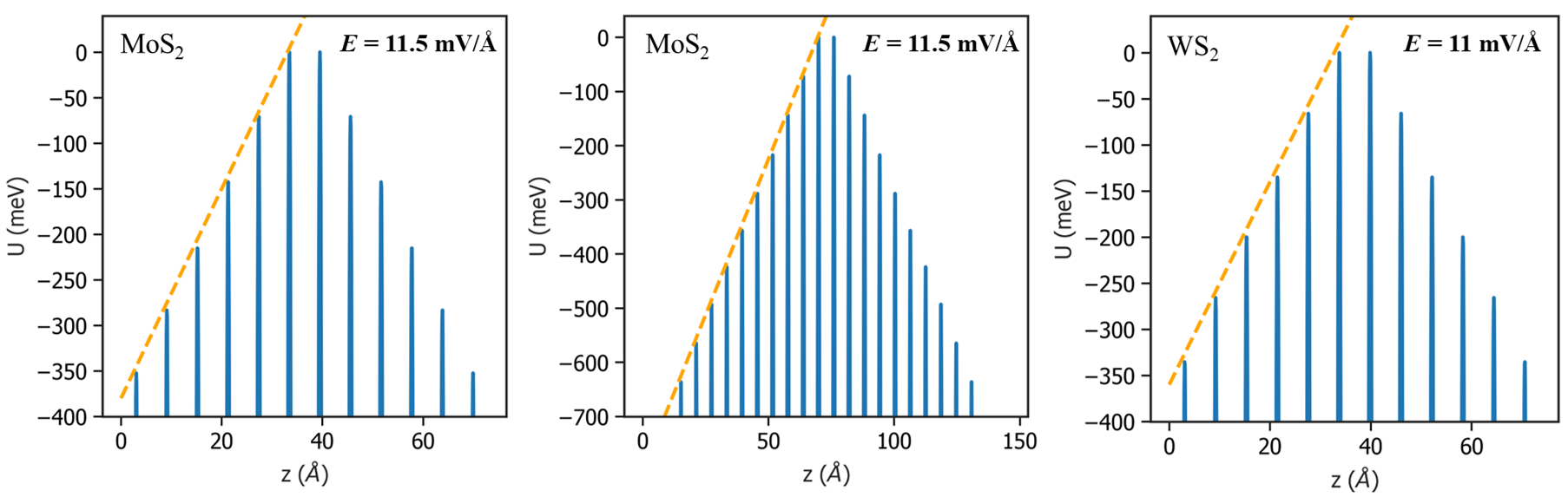
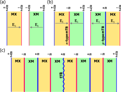
Interfacial ferroelectricity [1] has been recently identified as a peculiar feature of the rhombohedral polytype of semiconducting transition metal dichalcogenides (TMDs: MoS2, WS2, MoSe2, WSe2) [2, 3, 4]. For example, 3R-MoS2 and 3R-WS2 are layered van der Waals (vdW) crystals which have neither inversion nor mirror symmetry [5], permitting a c-axis ferroelectric (FE) polarization, which is, indeed, generated by the interlayer charge transfer induced by weak hybridization of chalcogen orbitals [6, 7, 8, 9]. The direction of such polarization is determined by the stacking of consecutive layers, identified as metal-over-chalcogen (MX) and chalcogen-over-metal (XM) configurations (see Fig. 1). The above relation between stacking order and FE polarization, demonstrated in a number of experiments involving TMD bilayers, where polarization inversion was produced by sliding of adjacent TMD monolayers [1, 10, 11], also suggests better stability of FE domains in vdW ferroelectrics, as compared to conventional FE crystals [12]. Potential steps of or , for MX or XM domains respectively (caused by the double layer of charge at the interface of consecutive monolayers), generate staircase potential profiles inside these domains, Fig. 1, which can be associated with a built-in electric field inside MX and XM twins.
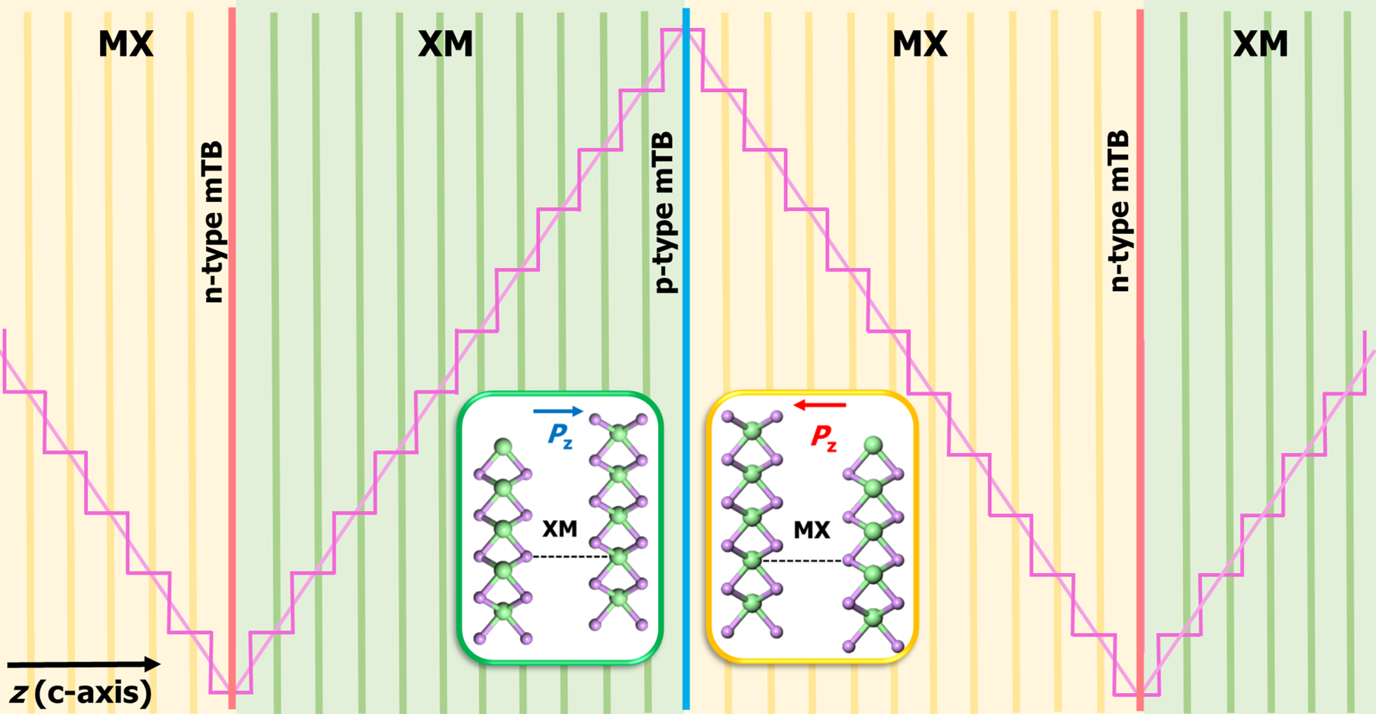
In general, a piece of bulk FE material would contain domains of alternating electrical polarization, separated by domain walls [12]. In ferroelectric MX2, polarisation domains are nothing but structural MX- and XM-stacking twins, separated by mirror twin boundaries (mTBs). For electrons and holes, these mTBs represent maxima and minima of quantum wells hosting two-dimensional (2D) electrons or holes (which can, for example, be separated upon photo-excitation). Here, we predict that such twin boundaries can hold charge carriers with a density of up to , which can be achieved by photo-doping at cryogenic temperatures [13, 14], and perform self-consistent analysis of the binding energies and quantum well wave functions to identify the twin structures which are most favourable for the formation of 2D electron layers in thin films of rhombohedral MoS2 and WS2.
To describe the FE potential profile in a twinned bulk 3R-MX2, we have performed ab initio DFT, implemented in the Quantum ESPRESSO package [15, 16], analysing bulk supercells consisting of up to 12 layers per twin. Plane-wave kinetic energy cutoffs of 80 and 800 Ry were applied for wavefunction and charge density expansions, respectively, and the Brillouin zone was sampled using a Monkhorst-Pack uniform k-point grid for all structures. The exchange-correlation effects were approximated by the generalised gradient approximation (GGA) using the Perdew-Burke-Ernzerhof (PBE) functional [17, 18]. Ultrasoft pseudopotentials were used to approximate the interaction between nucleus and electrons [19, 20], and the vdW-DF2-C09 functional was implemented to compute interlayer adhesion for relaxing the lattice [21, 22, 23, 24], using the Broyden–Fletcher–Goldfarb–Shanno (BFGS) quasi-Newton algorithm. Non-collinear spin-orbit coupling (SOC) was incorporated into all band structure calculations via ultra-soft fully relativistic pseudo-potentials [25]. In particular, this gives us the layer-resolved potentials across the studied structures (examples shown in Extended Data Fig. 1), consistent with the individual ‘double-charge-layer’ potential steps found in bilayers [26, 2] and few-layer mixed-stacking crystals [27].
| e/h in mTB and h in tTB | e/h in the surface and e in tTB | ||||||||||||
| [V/] | [] | [] | [nm] | [meV] | [meV] | [meV] | [meV] | [meV] | [meV] | [meV] | [meV] | ||
| MoS2 | e | 0.115 | 0.8 | 0.51 | 1.09 | 72.4 | 106.4 | 34.0 | 10.0 | 198.8 | 227.8 | 29.0 | 5.0 |
| h | 0.88 | 0.91 | 60.4 | 88.7 | 28.4 | 27.7 | 164.8 | 188.9 | 24.1 | 12.6 | |||
| WS2 | e | 0.110 | 0.8 | 0.48 | 1.13 | 71.7 | 105.4 | 33.7 | 11.1 | 196.9 | 225.7 | 28.8 | 5.5 |
| h | 0.84 | 0.97 | 61.8 | 90.9 | 29.1 | 27.9 | 161.5 | 185.1 | 23.6 | 13.6 | |||
From this, we evaluate the intrinsic ferroelectric field in 3R-MoS2 and 3R-WS2, (as the envelope of the on-layer potentials) and estimate a 2D charge that would compensate the intrinsic field (see Table 1) and set up an electrostatic limit for the maximum carrier density that can be held by the twin boundary,
| (1) |
Here, is the c-axis (out-of-plane) dielectric constant of TMD (6.1 in MoS2 and 5.8 in WS2, according to Refs. 28, 27), is the vacuum electric permittivity, and is the electron charge, leading to cm-2 for both MoS2 and WS2. We note that mono-twin film surfaces would hold maximum carrier density , so that internal mTBs follow a rule of sum for surface layer densities of the constituent twinned crystals, as sketched in Extended Data Fig. 2. In addition, one can mechanically assemble two FE films, thus, creating a twisted twin boundary (tTB): such an interface would hold the same maximum charge carrier density as an untwisted mTB.
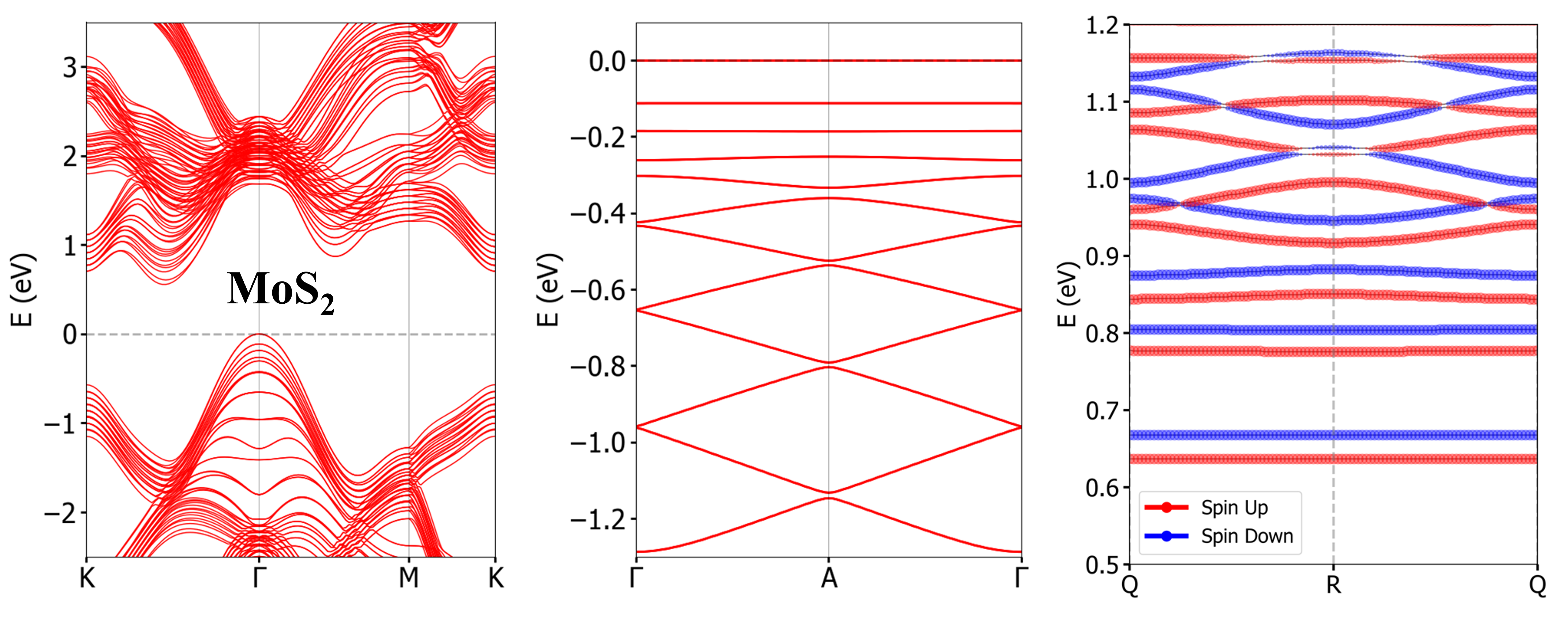
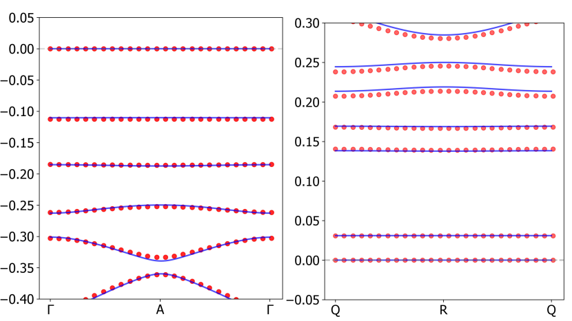
To determine self-consistent binding energies and compare those with the Fermi level of carriers with the accumulated density, we computed the effective masses () for Q-point electrons in the conduction band and -point valence band holes (and spin-orbit splitting, , for the Q-point band edge). The in-plane masses were found by fitting the band edge energy profile (e.g., in Extended Data Fig. 3) to a parabolic dispersion, and appear to be quite heavy. In contrast, c-axis effective mass, , required a more elaborate approach, due to the FE potential. We determined by solving the one-dimensional Schrödinger equation for a particle of mass in a periodic sawtooth potential (given by ) for a bulk crystal composed of 12-layer twins and comparing its spectrum to the DFT-computed -dispersions near the conduction and valence band edges (see in Methods and Extended Data Figs. 3, 4). The obtained values are listed in Table I.
To analyse self-consistent screening of the underlying FE electric field by the accumulated charge carriers, we assume that all carriers occupy the lowest subband in the resulting quantum well (this assumption is, then, checked by comparing the computed subband and Fermi energies). This involves solving the Thomas-Fermi problem,
where is the overall electrostatic potential, and is the wavefunction of the lowest energy bound state in the quantum well at an energy for electrons (e - top signs) and holes (h - bottom signs). The electrostatic boundary conditions at mTB, surface, and tTB – both for n- and p-type accumulation layers – are set as , , and at the surface () and in the middle of MX and XM twins (), respectively. In contrast, boundary conditions for electron/hole wave functions depend on the type of interface/surface. For a mTB, DFT results suggest that wavefunctions of both electrons and holes are continuous and smooth across the twin boundary, because of matching band edges in MX and XM crystals, hence for the lowest-energy state. At the external surface, for both types of charge carriers. Finally, the interlayer twist at a tTB produces different boundary conditions for the two types of charge carriers: for holes with the band edge at the -point, twist does not obstruct inter-layer hybridisation, so that boundary conditions are the same as for a non-twisted interface, whereas for electrons twist generates a momentum mismatch between Q-point band edges in MX and XM twins which suppresses interlayer hybridization, separating the quantum well into two – one on the MX and the other on XM side – with at the interface.
To solve this self-consistent problem, we introduce a length, , and scaling , , and , where variables and and function are dimensionless. Then, we solve numerically the following non-linear integro-differential equation:
| (2) | |||
The normalisation of in this equation reflects the sum rule of surface charges illustrated in Extended Data Fig. 2 (note that Eq. (3) is formulated in half-space), and dimensionless function gives the self-consistent potential profile, . This enables us to describe both electrons and holes simultaneously in all FE MX2 materials.
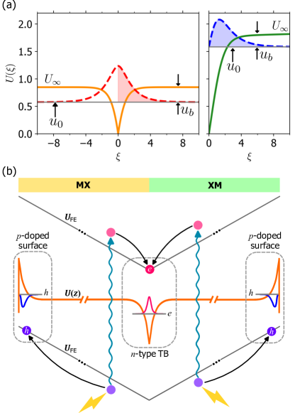
Two solutions of Eq. (2), obtained by the shooting procedure described in Methods, one with boundary condition (I) and the other (II) with , are shown in Fig. 2a. These solutions encompass all accumulation layers we discuss in this paper: mTB, surfaces and tTB. Solution I (shown in left panel of Fig 2a and applicable to electrons at mTB and holes at mTB and tTB), produces (which determines the energy of the ground state in the well), with binding energy determined by a parameter (obtained as a difference between and ). Solution II, r.h.s. panel of Fig 2a, is and applicable to electrons at tTB and electrons and holes at surfaces and produces and .
Using scaling rules and material parameters in Extended Data Table I, we estimate binding energies for accumulation layers of electrons and holes at mTB, tTB and surfaces for 3R-MoS2 and 3R-WS2, which are gathered in Table I. Here we note that a typical extent of the computed localised states is about nm, which covers about 6 layers: this justifies the use of a continuum description in the confinement problem. To discuss stability of the 2D accumulation layers, we compare the computed binding energies, , with the Fermi energies (Table I) of 2D carriers with corresponding in-plane masses, (see Extended Data Table I). In these estimates, we account for the spin-degeneracy factors for -point holes and spin-polarised Q valleys for electron at mTB and surface states. We also note that for electrons at tTBs, reflecting the contribution from two sets of mismatched Q points in the misaligned MX- and XM-stacking crystals. Also, we note that in all cases the next level in the quantum well is pushed up into the continuum spectrum, which justifies the use of the assumption that all electrons/hole are in the lowest subband of the resulting quantum well.
When we compare the computed values of and in Table I, we find that the higher degeneracy factor for electrons makes their accumulation at both mTB and surfaces stable at cryogenic temperatures, 100K. In contrast, for holes at mTB, , making easier their evaporation into bulk, potentially, resulting in a temperature-dependent multi-subband accumulation layer (essentially, a 3D system). However, for the p-type surface states, meV in both MoS2 and WS2, suggesting that a thin film with a single MX/XM twin boundary would be an ideal host for a 2D electron channel. This system is illustrated in Fig. 2b, where we also suggest to use photo-excitation of free electron-hole pairs [13, 14] to induce the mTB-surface charge separation, thus, avoiding a dependency on the 2D channel formation on the material doping.
An even more exciting opportunity is offered by a n-type twisted twin boundary (tTB) in a film assembled from two oppositely polarised mono-twin films with misaligned orientation of crystalline axes. As compared to bulk vdW crystals, where twinned structures are formed by chance during the non-equilbrium conditions of crystal growth, the polarisation of domains and orientation of the MX/XM boundary in twistronic structures can be engineered in the course of their assembly. In this case, the control of the twist angle (e.g., by ‘folding’ a mono-twin film against a properly chosen axis) gives access to moiré patterns with potential for commensurability between their periodicity and carrier density, . Another advantage of the assembled structures is that graphene, embedded at the ends, can be used to contact the electrons at the tTB, and graphene top/bottom gates can be added to access fine tuning of the tTB carrier density.
For twistronic films assembled with an almost parallel orientation (P) of unit cells, e.g., as if folding a mono-twin crystal against its armchair direction, the superlattice at the twisted interface would be analogous to a triangular lattice of alternating local XM and MX stacking areas, essentially, relocating the twin boundary up and down by one layer. Then, a natural commensurability condition for such a superlattice corresponds to two electrons per moiré supercell and a ‘magic’ twist angle . For a film assembled by ‘folding’ a mono-twin film against its zig-zag axis, producing an almost antiparallel orientation (AP) of unit cells – ‘rotation angle’ – the superlattice at the tTB would be analogous to a triangular lattice with periodically appearing 2H-stacking areas. In that case, the commensurability condition would correspond to one electron per moiré superlattice unit cell, which would be provided by a larger ‘magic’ twist angle , as listed in Table II.
Also, Table II contains values of the Wigner parameter, , which characterises the strength of electron-electron interaction in 2D metals [29]. To estimate it, we used effective masses listed in Extended Data Table I, and effective dielectric constant, , for inner interfaces (with the in-plane component [28] of the dielectric tensor of TMDs), whereas for surface states we assumed an hBN encapsulation and used . Due to the large doping densities, we find , which suggests that interactions are strong but insufficient to crystallise electrons on their own. However, for the tTB electrons, one can use a magic twist angle, , to promote electrons’ Wigner crystallisation with (natural for 2D systems [30, 31, 32, 33]) triangular lattice by making commensurate with moiré superlattice at the corresponding P/AP interface.
| mTB & tTB | Surface | |||
|---|---|---|---|---|
| MoS2 | e | 2.4 | 3.4 | |
| h | 2.6 | 4.0 | ||
| WS2 | e | 2.4 | 3.5 | |
| h | 2.7 | 3.8 | ||
Overall, we propose a new type of 2D electron systems, formed by the accumulation of heavy electrons at twin boundaries in ferroelectric van der Waals semiconductors, such as rhombohedral MoS2 and WS2. The presented analysis also highlights the prospects offered by twistronic structure, assembled by combining two mono-twin films, for creating strongly correlated states of 2D electrons at the magic-angle twisted twin boundaries.
Methods
Structural relaxation
DFT calculations were performed using both bulk 2H and 3R TMDs. For 3R-MoS2 and 3R-WS2, mTB structures were created by iterated shifting of adjacent parallel layers in bulk by , with sign reversed between the two domains, which was performed for domains with 6, 9 and 12 layers in each domain. Optimisation was performed until energies and forces had converged to a tolerance of Ry and Ry/a0, respectively. A dense k-point grid of was used to sample 2H bulk structures, while a grid was used for mTB structures with large c-axis DFT supercell dimensions. As shown in Extended Data Table I, the interlayer spacings (M-M distances) of MoS2, WS2 twin boundaries are 6.078 and 6.133 respectively, which have are comparable to the 2H-MX2 interlayer spacing.
Intrinsic electric field and out-of-plane masses of electrons and holes
We calculate the ferroelectric field inside twins by approximating the staircase of interlayer potential steps for 6, 9 and 12 layer domains (see Fig. 1) as . This gives us a value of mV/ for MoS2, and mV/ for WS2, in agreement with the earlier calculated double layer potentials in bilayers [26].
After this, electronic band structures for these multilayers (computed taking into account spin-orbit coupling) were used to determine in-plane ( - by parabolic fitting) and out-of-plane () effective masses. The c-axis mass, , was determined using the energies of several lowest minibands in periodic mTB with 6, 9 and 12 layers in each twin (examples for a 6+6 superstructure is shown in Extended Data Fig. 4 for VB and CB respectively). Then, non-dispersive -bands were approximated with the energy spectrum of a triangular potential well with a slope corresponding to the intrinsic field , simultaneously, compared (see Extended Data Fig. 4) to the DFT dispersion of a 6-layer mTB cell with a dispersion of an electron with the extracted effective mass in the equivalent sawtooth potential. The same procedure was implemented for WS2. The obtained c-axis mass, , are lighter than the corresponding c-axis masses in bulk 2H crystals.
Multi-parameter shooting method to solve Thomas-Fermi problem
Solutions for the integro-differential equation (2) in the main text are found by employing a shooting method: that is we integrate it from relevant boundary conditions ( and for case I, and and for case II) at up to , varying the parameter until we reach a solution that acquires at the end of the interval without changing sign within it.
Due to the non-linearity of this equation, the initial values of and are not irrelevant free parameters as it would be for a linear Schrödinger equation. Here, they are involved in determining the normalization factor of the function , . Therefore we continuously vary the parameters and with small steps and identify their values for which the normalization factor becomes (see Extended Data Fig. 5).
Finally, we verify the shooting results by using a finite difference method, where the problem is solved iteratively: the solution to the triangular potential is taken as the starting point to compute a new potential , from which a self-consistent cycle follows until convergence is reached in the value of . The evolution of as a function of the number of iterations for case I is shown as an inset in Extended Data Fig. 5(a), where the convergence value agrees exactly with the one obtained via the shooting method.
Acknowledgements
The authors thank Z. Sofer, I. Rozhansky, R. Gorbachev and A. Geim for fruitful discussions. I.S. and X.L. acknowledge financial support from the University of Manchester’s Dean’s Doctoral Scholarship. This work was supported by the EC-FET Core 3 European Graphene Flagship Project, EC-FET Quantum Flagship Project 2D-SIPC, EPSRC Grants EP/S030719/1 and EP/V007033/1, and the Lloyd Register Foundation Nanotechnology Grant. Calculations were performed using the Sulis Tier 2 HPC platform hosted by the Scientific Computing Research Technology Platform at the University of Warwick and funded by EPSRC Grant EP/T022108/1 and the HPC Midlands+ consortium.
Author contributions
V.I.F. conceived the idea of the project and designed its methodology. X.L. and J.G.M. performed DFT modelling and determined input parameters for the mesoscale model and the Thomas-Fermi problem, which was solved numerically by I.S. All authors were involved in discussions and contributed equally to writing the manuscript.
References
- Vizner Stern et al. [2021] M. Vizner Stern, Y. Waschitz, W. Cao, I. Nevo, K. Watanabe, T. Taniguchi, E. Sela, M. Urbakh, O. Hod, and M. Ben Shalom, Interfacial ferroelectricity by van der Waals sliding, Science 372, 1462–1466 (2021).
- Weston et al. [2022] A. Weston, E. G. Castanon, V. Enaldiev, F. Ferreira, S. Bhattacharjee, S. Xu, H. Corte-León, Z. Wu, N. Clark, A. Summerfield, T. Hashimoto, Y. Gao, W. Wang, M. Hamer, H. Read, L. Fumagalli, A. V. Kretinin, S. J. Haigh, O. Kazakova, A. K. Geim, V. I. Fal’ko, and R. Gorbachev, Interfacial ferroelectricity in marginally twisted 2D semiconductors, Nature Nanotechnology 17, 390–395 (2022).
- Enaldiev et al. [2021] V. V. Enaldiev, F. Ferreira, S. J. Magorrian, and V. I. Fal’ko, Piezoelectric networks and ferroelectric domains in twistronic superlattices in WS2/MoS2 and WSe2/MoSe2 bilayers, 2D Materials 8, 025030 (2021).
- Wang et al. [2022] X. Wang, K. Yasuda, Y. Zhang, S. Liu, K. Watanabe, T. Taniguchi, J. Hone, L. Fu, and P. Jarillo-Herrero, Interfacial ferroelectricity in rhombohedral-stacked bilayer transition metal dichalcogenides, Nature Nanotechnology 17, 367–371 (2022).
- Strachan et al. [2021] J. Strachan, A. F. Masters, and T. Maschmeyer, 3R-MoS2 in Review: History, Status, and Outlook, ACS Applied Energy Materials 4, 7405–7418 (2021).
- Wang et al. [2017] Y. Wang, Z. Wang, W. Yao, G.-B. Liu, and H. Yu, Interlayer coupling in commensurate and incommensurate bilayer structures of transition-metal dichalcogenides, Physical Review B 95, 10.1103/physrevb.95.115429 (2017).
- Li and Wu [2017] L. Li and M. Wu, Binary compound bilayer and multilayer with vertical polarizations: Two-dimensional ferroelectrics, multiferroics, and nanogenerators, ACS Nano 11, 6382–6388 (2017).
- Tong et al. [2020] Q. Tong, M. Chen, F. Xiao, H. Yu, and W. Yao, Interferences of electrostatic moiré potentials and bichromatic superlattices of electrons and excitons in transition metal dichalcogenides, 2D Materials 8, 025007 (2020).
- Wu [2021] M. Wu, Two-Dimensional van der Waals Ferroelectrics: Scientific and Technological Opportunities, ACS Nano 15, 9229–9237 (2021).
- Meng et al. [2022] P. Meng, Y. Wu, R. Bian, E. Pan, B. Dong, X. Zhao, J. Chen, L. Wu, Y. Sun, Q. Fu, Q. Liu, D. Shi, Q. Zhang, Y.-W. Zhang, Z. Liu, and F. Liu, Sliding induced multiple polarization states in two-dimensional ferroelectrics, Nature Communications 13, 10.1038/s41467-022-35339-6 (2022).
- Van Winkle et al. [2024] M. Van Winkle, N. Dowlatshahi, N. Khaloo, M. Iyer, I. M. Craig, R. Dhall, T. Taniguchi, K. Watanabe, and D. K. Bediako, Engineering interfacial polarization switching in van der Waals multilayers, Nature Nanotechnology 10.1038/s41565-024-01642-0 (2024).
- Meier and Selbach [2021] D. Meier and S. M. Selbach, Ferroelectric domain walls for nanotechnology, Nature Reviews Materials 7, 157–173 (2021).
- Yang et al. [2022] D. Yang, J. Wu, B. T. Zhou, J. Liang, T. Ideue, T. Siu, K. M. Awan, K. Watanabe, T. Taniguchi, Y. Iwasa, et al., Spontaneous-polarization-induced photovoltaic effect in rhombohedrally stacked mos2, Nature Photonics 16, 469 (2022).
- Wu et al. [2022] J. Wu, D. Yang, J. Liang, M. Werner, E. Ostroumov, Y. Xiao, K. Watanabe, T. Taniguchi, J. I. Dadap, D. Jones, et al., Ultrafast response of spontaneous photovoltaic effect in 3r-mos2–based heterostructures, Science Advances 8, eade3759 (2022).
- Giannozzi et al. [2009] P. Giannozzi, S. Baroni, N. Bonini, M. Calandra, R. Car, C. Cavazzoni, D. Ceresoli, G. L. Chiarotti, M. Cococcioni, I. Dabo, A. D. Corso, S. de Gironcoli, S. Fabris, G. Fratesi, R. Gebauer, U. Gerstmann, C. Gougoussis, A. Kokalj, M. Lazzeri, L. Martin-Samos, N. Marzari, F. Mauri, R. Mazzarello, S. Paolini, A. Pasquarello, L. Paulatto, C. Sbraccia, S. Scandolo, G. Sclauzero, A. P. Seitsonen, A. Smogunov, P. Umari, and R. M. Wentzcovitch, Quantum ESPRESSO: a modular and open-source software project for quantum simulations of materials, Journal of Physics: Condensed Matter 21, 395502 (2009).
- Giannozzi et al. [2017] P. Giannozzi, O. Andreussi, T. Brumme, O. Bunau, M. B. Nardelli, M. Calandra, R. Car, C. Cavazzoni, D. Ceresoli, M. Cococcioni, N. Colonna, I. Carnimeo, A. D. Corso, S. de Gironcoli, P. Delugas, R. A. DiStasio, A. Ferretti, A. Floris, G. Fratesi, G. Fugallo, R. Gebauer, U. Gerstmann, F. Giustino, T. Gorni, J. Jia, M. Kawamura, H.-Y. Ko, A. Kokalj, E. Küçükbenli, M. Lazzeri, M. Marsili, N. Marzari, F. Mauri, N. L. Nguyen, H.-V. Nguyen, A. O. de-la Roza, L. Paulatto, S. Poncé, D. Rocca, R. Sabatini, B. Santra, M. Schlipf, A. P. Seitsonen, A. Smogunov, I. Timrov, T. Thonhauser, P. Umari, N. Vast, X. Wu, and S. Baroni, Advanced capabilities for materials modelling with Quantum ESPRESSO, Journal of Physics: Condensed Matter 29, 465901 (2017).
- Grimme [2006] S. Grimme, Semiempirical GGA‐type density functional constructed with a long‐range dispersion correction, Journal of Computational Chemistry 27, 1787–1799 (2006).
- Perdew et al. [1996] J. P. Perdew, K. Burke, and M. Ernzerhof, Generalized Gradient Approximation Made Simple, Phys. Rev. Lett. 77, 3865 (1996).
- Blöchl [1994] P. E. Blöchl, Projector augmented-wave method, Phys. Rev. B 50, 17953 (1994).
- Kresse and Joubert [1999] G. Kresse and D. Joubert, From ultrasoft pseudopotentials to the projector augmented-wave method, Phys. Rev. B 59, 1758 (1999).
- Lee et al. [2010] K. Lee, E. D. Murray, L. Kong, B. I. Lundqvist, and D. C. Langreth, Higher-accuracy van der waals density functional, Phys. Rev. B 82, 081101 (2010).
- Cooper [2010] V. R. Cooper, Van der waals density functional: An appropriate exchange functional, Phys. Rev. B 81, 161104 (2010).
- Novais Antunes et al. [2018] F. P. Novais Antunes, V. S. Vaiss, S. R. Tavares, R. B. Capaz, and A. A. Leitão, Van der waals interactions and the properties of graphite and 2h-, 3r- and 1t-mos2: A comparative study, Computational Materials Science 152, 146–150 (2018).
- Conte et al. [2019] F. Conte, D. Ninno, and G. Cantele, Electronic properties and interlayer coupling of twisted heterobilayers, Phys. Rev. B 99, 155429 (2019).
- Husain et al. [2020] S. Husain, R. Gupta, A. Kumar, P. Kumar, N. Behera, R. Brucas, S. Chaudhary, and P. Svedlindh, Emergence of spin–orbit torques in 2d transition metal dichalcogenides: A status update, Applied Physics Reviews 7, 10.1063/5.0025318 (2020).
- Ferreira et al. [2021] F. Ferreira, V. V. Enaldiev, V. I. Fal’ko, and S. J. Magorrian, Weak ferroelectric charge transfer in layer-asymmetric bilayers of 2d semiconductors, Scientific Reports 11, 10.1038/s41598-021-92710-1 (2021).
- Ferreira et al. [2022] F. Ferreira, V. V. Enaldiev, and V. I. Fal’ko, Scaleability of dielectric susceptibility with the number of layers and additivity of ferroelectric polarization in van der waals semiconductors, Phys. Rev. B 106, 125408 (2022).
- Laturia et al. [2018] A. Laturia, M. L. Van de Put, and W. G. Vandenberghe, Dielectric properties of hexagonal boron nitride and transition metal dichalcogenides: from monolayer to bulk, npj 2D Materials and Applications 2, 10.1038/s41699-018-0050-x (2018).
- Giuliani and Vignale [2008] G. Giuliani and G. Vignale, Quantum theory of the electron liquid (Cambridge university press, 2008).
- Smoleński et al. [2021] T. Smoleński, P. E. Dolgirev, C. Kuhlenkamp, A. Popert, Y. Shimazaki, P. Back, X. Lu, M. Kroner, K. Watanabe, T. Taniguchi, I. Esterlis, E. Demler, and A. Imamoğlu, Signatures of wigner crystal of electrons in a monolayer semiconductor, Nature 595, 53–57 (2021).
- Zhou et al. [2021] Y. Zhou, J. Sung, E. Brutschea, I. Esterlis, Y. Wang, G. Scuri, R. J. Gelly, H. Heo, T. Taniguchi, K. Watanabe, et al., Bilayer wigner crystals in a transition metal dichalcogenide heterostructure, Nature 595, 48 (2021).
- Regan et al. [2020] E. C. Regan, D. Wang, C. Jin, M. I. Bakti Utama, B. Gao, X. Wei, S. Zhao, W. Zhao, Z. Zhang, K. Yumigeta, et al., Mott and generalized wigner crystal states in wse2/ws2 moiré superlattices, Nature 579, 359 (2020).
- Padhi et al. [2021] B. Padhi, R. Chitra, and P. W. Phillips, Generalized wigner crystallization in moiré materials, Physical Review B 103, 125146 (2021).
- Bronsema et al. [1986] K. D. Bronsema, J. L. De Boer, and F. Jellinek, On the structure of molybdenum diselenide and disulfide, Zeitschrift für anorganische und allgemeine Chemie 540, 15–17 (1986).
- Schutte et al. [1987] W. Schutte, J. De Boer, and F. Jellinek, Crystal structures of tungsten disulfide and diselenide, Journal of Solid State Chemistry 70, 207–209 (1987).
Extended Data
| (expt) | (expt) | // | |||||||
|---|---|---|---|---|---|---|---|---|---|
| [Å] | [Å] | [Å] | [Å] | [V/nm] | [] | [meV] | |||
| MoS2 | 2H | 3.151 | 6.121 | 3.160 [34] | 6.147 [34] | 0.115 | 0.51/0.75/0.51 | 31 | |
| 3R | 3.154 | 6.079 | - | - | -0.67/-0.67/-0.88 | 0 | |||
| WS2 | 2H | 3.155 | 6.153 | 3.153 [35] | 6.162 [35] | 0.110 | 0.53/0.56/0.48 | 150 | |
| 3R | 3.158 | 6.133 | 3.158 [35] | 6.136 [35] | -0.61/-0.61/-0.75 | 0 |