Optimal Switching Networks for Paired-Egress Bell State Analyzer Pools ††thanks: This work was supported by JST [Moonshot R&D Program] Grant Numbers [JPMJMS226C] and [JPMJMS2061].
Abstract
To scale quantum computers to useful levels, we must build networks of quantum computational nodes that can share entanglement for use in distributed forms of quantum algorithms. In one proposed architecture, node-to-node entanglement is created when nodes emit photons entangled with stationary memories, with the photons routed through a switched interconnect to a shared pool of Bell state analyzers (BSAs). Designs that optimize switching circuits will reduce loss and crosstalk, raising entanglement rates and fidelity. We present optimal designs for switched interconnects constrained to planar layouts, appropriate for silicon waveguides and Mach-Zehnder interferometer (MZI) switch points. The architectures for the optimal designs are scalable and algorithmically structured to pair any arbitrary inputs in a rearrangeable, non-blocking way. For pairing inputs, switches are required, which is less than half of number of switches required for full permutation switching networks. An efficient routing algorithm is also presented for each architecture. These designs can also be employed in reverse for entanglement generation using a shared pool of entangled paired photon sources.
Index Terms:
Quantum Network, Fault-Tolerant Quantum Computing, Interconnect Networks, Switched-BSA, Planar Architecture, Photonic Chip, Photonic Switch, Heralded Entanglement GenerationI Introduction
The importance of switching of signals has been understood since the earliest days of telecommunications. The mid-twentieth century saw advances in both the practice and theory of switching for telephone networks, resulting in multi-stage designs such as Clos, Benes̆, omega and butterfly networks for electrical signals, coupling small switch units together via discrete wires or coaxial cables [1, 2, 3, 4, 5]. Inspired by these designs, and facing the need to scale up systems, computer architects have built multicomputers, systems with many independent processors and memory units connected via interconnection networks [6, 3, 7, 8]. Multicomputer designs for quantum computers, in which a number of independent quantum computers with separate quantum registers and control systems are coupled via an interconnect network, are widely seen as a necessary architectural approach to achieving scalable, fault-tolerant systems [9, 10, 11, 12, 13, 14, 15, 16, 17, 18, 19, 20, 21]. For multicomputer quantum processing of transferring quantum state (teledata) or performing teleportation of quantum gates (telegate), the ability to generate Bell pairs and deliver them to arbitrary quantum processing units is essential [22, 23, 24].
In addition to the architectural challenges of solving a large scale quantum algorithm using a quantum multicomputer, the cooperative nature of some distributed quantum algorithms over a structured quantum network requires an efficient interconnect between quantum nodes in the network. To achieve scalability, the unrealistic, abstract model with direct interfaces between every pair of quantum computers or nodes in the network must be replaced with a realistic switch interconnect architecture [8, 25] to have reconfigurable paths between arbitrary nodes. Switching interconnects are also indispensable components of a number of quantum network testbed designs that are planned to be deployed in the near future [26, 27], paving the way to the eventual quantum Internet [28, 29, 30, 31, 32].
The primary service of quantum networks is the distribution of entangled states, usually entangled pairs of qubits. This departure from the packet-forwarding or circuit-switching nature of classical networks presents a unique set of challenges for the design of quantum switching networks, with the goal of distributing pairs of entangled photons to the terminals.
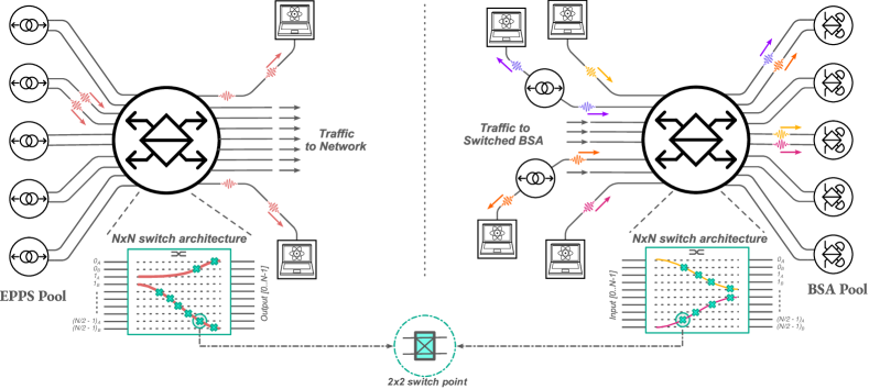
One approach to quantum switching interconnects assumes the availability of a shared pool of entangled photon-pair sources (EPPS Pool) as pictured in the left panel of Fig. 1. In this architecture, pairs of entangled photons are generated at the EPPS nodes and routed by the optical switch to the appropriate end nodes. This demonstrates the fundamental difference between classical and quantum switching interconnects. In the EPPS Pool architecture, initially neighboring inputs (entangled photon pairs) must be switched to an arbitrary pair of outputs. A non-planar optimal solution to this problem was proposed by Drost et al. [33] for cases up to 1010 quantum switches. This solution was found via exhaustive search but did not provide a good recursive design that would lead to optimal and scalable quantum switching networks.
Optimal planar and scalable designs for full permutation switching networks are over-designed for the problem of pair matching as they require the ability to route all input-output combinations. The ability to route photons to arbitrary BSAs, including arbitrary choice of the BSA ports, is not required for successful execution of entanglement swapping between desired pairs of photons.
We consider the inverse problem to the EPPS Pool architecture, shown in the right panel of Fig. 1. Photons originating from the quantum network are inputs into the quantum switch, which routes the desired pairs of photons to be incident onto the same Bell State Analyzer (BSA). The pair of photons then undergoes a Bell-state measurement, leading to entanglement between the respective end nodes. The unique aspect of this BSA Pool architecture is that which BSA is used to perform entanglement swapping is irrelevant.
We propose three recursive designs for a planar quantum switch composed of a number of switch points. We obtain a lower bound for the number of switch points required for the quantum switch to be rearrangeably non-blocking, and demonstrate that all three of our designs saturate this lower bound. For each design, we present an efficient routing algorithm. We further analyze the depth of the three designs, and the average number of switch points that a photon traverses in order to better understand their loss properties. Finally, we compare our planar designs with existing planar [34] and non-planar solutions for quantum [33] as well as classical switches [4, 5], and demonstrate favourable scaling properties of our designs.
II Preliminaries
We begin by describing the basics of optical switching networks and how quantum networks differ from classical ones. We then proceed to summarize fabrication factors that place constraints on our design. Finally, we discuss the assumptions used in this work before ending this section with the problem statement.
II-A Classical and quantum optical switching networks
An optical switching network has a number of important characteristics that should be considered while designing a switching configuration:
-
•
Size: the number of input and output ports
-
•
Blocking/non-blocking: whether the network can handle all possible input/output combinations
-
•
Switching time: the reconfiguration time for the network
-
•
Propagation delay: the time needed for photons to cross the network
-
•
Insertion loss: the probability of losing photons when crossing the physical interface from the channel to the switching element, typically involving a fiber/air boundary or a fiber/chip interface (generally reported in dB)
-
•
Switching loss: the probability of losing photons within the switching element (generally reported in dB)
-
•
Crosstalk: the leakage of signal to undesired transmission paths (generally reported in dB)
-
•
Redundancy: whether or not connectivity is degraded if a switch point or link fails
-
•
Physical dimensions: especially important when considering integration into the system
-
•
Cost: often reported as per-port cost for large configurations
The above list is largely common between classical and quantum switching networks. In a classical network, within reason, loss can be compensated for by increasing input signal power. In the systems we are designing (Fig. 1), the networks instead carry single photons.
Loss becomes the most critical metric and increases as the photons pass through channels, interfaces and switch points.
Polarization may be critical in quantum networks (depending on choice of qubit representation), and it can be changed by each component. If the network itself can be built with enough stability that its effect on polarization can be characterized at infrequent intervals, network operation will be more efficient [35, 36, 37]. Moreover, in physical design, self-calibration can also be achieved by adding auxiliary optical components to the photonic core [38, 39].
Most of the above characteristics depend on the choice of physical fabrication technology, but from the architectural design point of view, the number of input ports, total number of switches, and circuit depth indirectly affect propagation delay, insertion loss, switching loss, crosstalk, physical dimensions and cost.
II-B Fabrication Considerations
For optical systems, we can build switching systems based on photonic integrated circuit (PIC) technology [40, 39], or via free-space propagation of light, e.g. using micro electro-mechanical system (MEMS) switches [41, 42]. PICs have relatively high loss per centimeter of waveguide, but have the advantage of fewer fiber/air or fiber/chip interfaces that must be crossed compared to designs that use discrete components for each switch point. In this paper, we focus on integrated circuits.
Photolithographic fabrication for waveguides [43] or photonic crystals [44, 45] results in planar layouts. Two waveguides can be run close to each other, resulting in switch units based on Mach-Zehnder interferometric techniques, allowing two photons to be routed straight through or swapped under programmatic control. Grids of these basic units take sets of inputs from one edge of a chip and route them to a set of outputs at the opposite edge of the chip.
Promising platforms for fabrication of integrated photonic circuit such as silicon on insulator [43], silica on silicon [45] and stoichiometric silicon nitride () [46] have different fabrication complexity, photon loss and index contrast with different supported wavelengths. These layouts are generally kept planar due to the difficulty of routing a waveguide off the substrate surface without significant loss [47]. Therefore, we focus exclusively on planar switch designs in this work.
II-C Assumptions
Following the discussion in Sec. II-A and Sec. II-B, we now outline the assumptions used in the rest of the paper. The switch waveguides carry individual photons generated from quantum memories or entangled photon pair sources. BSAs are located outside the switch, with each BSA being attached to two neighboring output ports of the switch. Photons are to be matched in pairs and routed to any available BSA (paired egress). Use of the switch occurs in independent rounds, between which the switch may be reconfigured. The design must be planar and non-blocking for all possible choices of input pairings. Switch points are based on switching elements compatible with basic building blocks in photonic integrated circuits. Photons are guided single-pass only, from one side of the switch to another, and without any recirculation.
Issues of achieving indistinguishability between the input photons, such as polarization maintenance, spectral properties and time of arrival of the photons at the BSA, are out of the scope for this work. Based on the above assumptions, we can define the problem to be addressed.
II-D Problem statement
Consider an switching network with input ports, with photons where photon comes in at the -th port, and output ports coupled to BSAs. A paired egress request is represented as a tuple , where , and we call the set of all required pairings , where and each appear exactly once.
We want to find a scalable, planar and rearrangeably non-blocking topology for a switching network composed of base switch points, and a corresponding efficient routing algorithm capable of handling an arbitrary pair list . The routing algorithm must provide the state of every switch point in the network, denoted by , where represent the switch at layer between line and ,
and a permuted list of photons where the two photons at index and of the list go into the same BSA (the ) after exiting the switch. The concept of a layer will be made more precise when we introduce our designs.
III Optimal number of switch points
In order to show that our proposed switching networks are optimal, we consider the minimum number of switch points required to pair all input photons. It is known that a classical planar switching network requires at least switch points to achieve all input-output permutations [34].
We adapt the techniques used in [34] for the case of paired-egress switching networks. In order to obtain the minimum number of switch points for the network to be rearrangeably non-blocking, we consider the worst case scenario, where always the two most distant input photons are required to be paired together. The list of pairings is therefore given by , , , and so on. Bringing the input photons and together means that we must swap with all the other input photons, requiring switch points. This is true regardless of which BSA is assigned to perform entanglement swapping on the input photons and . A sample path and its required swaps are shown in the lower portion of the right panel of Fig. 1. Bringing the next pair of photons, , together requires swaps. Continuing with this logic, the minimum number of swaps, and therefore switch points, is given by
| (1) |
We observe that the minimum number of switch points for a planar rearrangeably non-blocking network with paired egresses is less than half of that obtained in [34] for a classical switching network.
IV Triangular Design
We begin with the simplest planar configuration for a rearrangeable non-blocking switching network with the minimum number of switch points. From this point forward in the paper, all designs are assumed to be paired egress, so we dispense with the qualifier.
IV-A Architecture
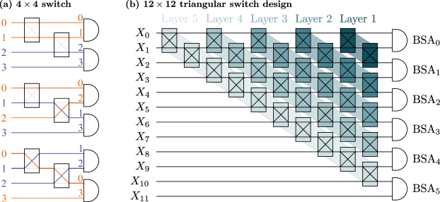
The smallest non-trivial switching network is a switch, shown in Fig. 2(a), and requires at least 2 switch points. By changing the state of the switch points, it is possible to achieve all possible input photon pairings. For example, leaving both switch points in the Bar state results in entanglement swapping between input photon pairs (0,1) and (2,3). Turning both of the switch points to Cross state routes the input photons in such a way that entanglement swapping is performed on the pairs (1,2) and (0,3).
This switch forms the basic building block for the triangular switch architecture, as depicted in Fig. 2(b). For input photons, the switch is composed of layers, where layer contains switch points. The total number of switch points is therefore given by
| (2) |
We see that the triangular architecture is optimal in terms of the number of switch points. The switch is constructed recursively by adding all switch points within a layer in a cascaded fashion. For layer , the switch points are arranged in the following way,
| (3) |
where represent the switch at layer between line and , as shown in Fig. 2(b) for the case of .
IV-B Routing
Showing that a switch design is rearrangeably non-blocking amounts to demonstrating that given a pair list , it is always possible to find a configuration of all switch points that permutes the input photon list such that all photon pairs are adjacent to each other. The routing algorithm strongly depends on the design of the switch. For the triangular design, it is relatively straightforward and is presented in Algorithm 1.
The input to the routing algorithm is given by the input photon list , and the pair list . The main strategy, similar to the bubble sort algorithm, is to start with photon since it is not incident onto any switch points and cannot be routed. We find its partner , such that , and configure the switch points in layer in order for the pair to meet on lines . This is achieved by setting all switch points , for to the Cross state. All other switch points in the layer, where , are set to the Bar state. The effect of this configuration leaves the ordering of photons unaffected, cascades the photon down to line , and shifts all remaining photons up by one unit. This process is next repeated for the next layer with input size , and the new list of photons until the input size becomes 2, reaching the trivial case.
For each layer, we traverse the photon list of length once and assign the switch states of switches. Therefore, the time complexity of this routing algorithm is .
Input: : indexable list ,
: set be paired
Output: permuted list:
Set of switch states
V Chevron Design
Our second switch design redistributes the switch points in a more uniform manner. This change leads to a more complicated, yet still efficient, routing algorithm.
V-A Architecture
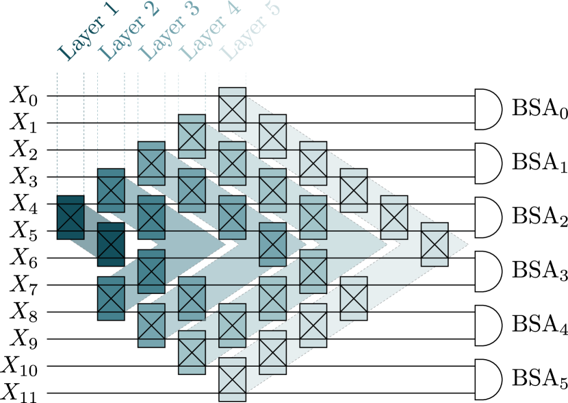
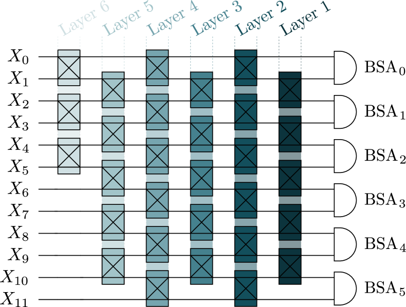
The chevron design is pictured in Fig. 3 for the case of . Similar to the triangular design, the chevron design consists of layers with layer consisting of switch points, resulting in the optimal number of total switch points . However, the switch points are laid out in a chevron, rather than a single diagonal arrangement.
For layer , with being even, half of the switch points in that layer are placed in the upper half of the chevron, with the rest of the switch points being placed in the bottom half. More precisely, the switch points in the upper half of a layer are placed as follows,
| (4) |
The switch points in the bottom half of the layer mirror the above arrangement,
| (5) |
For odd layers, the placement of the switch points is similar with the exception that the switch point is removed and a new switch point is placed at the tip of the chevron, as shown in Fig. 3.
V-B Routing
Algorithm 2 illustrates the procedure for determining switch status and the permuted list in the routing process. The routing algorithm for the chevron operates on the principle that if all photon pairs entering the last layer are adjacent to each other, except for two adjacent photons requiring pairing with the top- and bottom-most photons, the last chevron layer can handle their pairing. Alternatively, if all photons are already paired except for the top- and bottom-most photons, the algorithm can address this scenario as well. This approach is valid as we recursively go from layer to reducing the size of the switch from to by virtually pairing the photons that need to be matched with the top- and bottom-most photons until reaching the trivial inputs . This guarantees that at every recursion, all the photons will have a pairing within the considered range, either true or virtual pairings.
Determining where the pairs meet and which switch states to set at layer involves examining two different scenarios. First, consider the case where the top- and bottom-most photons form a pair, while the other photon pairs (either true or virtual) are already adjacent. In this scenario, all switch points in layer are set to Cross, causing the two outer photons to meet at the middle (, ) or (, ) when is odd or even, respectively. However, if the top- and bottom-most photons need to pair with two virtual pairings from the previous layer (on lines and ), and the virtual pair is oriented incorrectly, the switch point is set to Cross. Consequently, the two outer photons adjust to meet their partners, and if the pair resides in a different half (e.g., the top-most’s partner is in the bottom half), its partner also moves to meet the outer qubit at the middle. This results in only one switch point, aside from possibly , being set to Bar; when or otherwise, while the remaining switch points are set to Cross. All the possible scenarios and how the photons are moved are depicted in Fig. 4.
The runtime of the routing algorithm for the chevron architecture is . In each recursion, we go through the photon list only once to find partners of the top- and the bottom-most photons and all the switch states in the layer can then be decided just by knowing where the top- and bottom-most photons need to be moved to.
Input: : indexable list ,
: set of photons to be paired ,
: set of switch states (initially null set),
: indicating the start switch line considered in the recursion
Output: permuted list: ,
Set of switch states
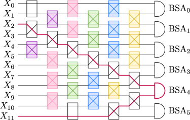
VI Brickwork Design
Our final design rearranges the switch points further into a brickwork pattern as shown in Fig. 5.
VI-A Architecture
This time, an switch consists of layers. There are three types of layers; odd, even, and the last layer. Unlike previous designs, the number of switch points inside a layer is independent of the layer number .
Odd layers contain switch points, while even layers contain switch points. The brickwork design is given by the following switch point placement,
| (6) | ||||
The exception to this rule is the final layer that contains switch points that are placed according to (6). The total number of switch points is therefore given by
| (7) |
which shows that the brickwork design is also optimal in terms of the number of switch points.
The brickwork design is similar to a full mesh structure of Spanke and Beneš in [34], with one difference. The full mesh architecture requires layers to perform full permutations, while in the brickwork design layers are sufficient for pairing an arbitrary input set.
VI-B Routing
The routing algorithm for pairing all the input photons in the brickwork design is shown in Algorithm 3. The underlying concept shares similarities with the Triangular design, but the process of removing switches is more intricate. First, we identify the partner photon of photon and progressively shift it downward to meet with . If the lowest line can reach is line , where , we also shift photon up to line . This method ensures that upon removing all utilized switch points and wire segments traversed by and , the resultant structure maintains a brickwork architecture, potentially with additional switch points in the last and second-to-last layers if the photon is shifted with the earliest switch points it encounters while is shifted as late as possible. These extra switch points can be configured to the Bar state, allowing for further recursion of the same routing algorithm until we reach the trivial photon parings.
Inputs: : indexable list ,
: set of tuple photons to be paired ,
: set of switch states (initially null set)
Outputs: Permuted list: ,
Set of switch states
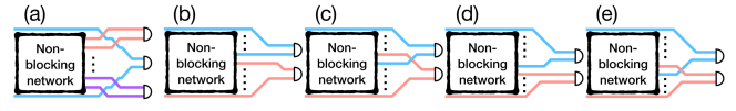
A sample routing round for pairing two photons ( with ) in a brickwork switch is shown in Fig. 6. Given that the distance between and exceeds making it impossible for the pair to meet on line , requiring that both photons must move to pair up on the closest line to , which is . By applying move as soon as possible routing policy for and move as late as possible routing policy for results in the desired permuted list . We have now assigned nine switch states, leaving the switch points into a brickwork design of smaller size with being an extra switch. Therefore, as shown in top-left side of Fig. 6, we set it to the Bar state. These two move policies guarantee that after pairing the last unpaired photon with its partner will leave the switch in the Brickwork design and thus allowing the smaller Brickwork to be routed the same way.
Similar to routing algorithms in triangular and chevron designs, we traverse the photon list once per iteration, thus the runtime of the routing algorithm in brickwork design is also .
VII Discussion
Having demonstrated that our three proposed planar designs are optimal and rearrangeable non-blocking, we now turn to a more detailed analysis of their depth properties. The depth is directly related to the expected losses of the switching network. We are not aware of any work considering planar designs for paired-egress outputs, making direct comparison impossible. To place our work into the larger context of other switching network designs, we consider existing planar and non-planar designs, as well as classical permutation networks and shared EPPS pool networks.
VII-A Switching network depth
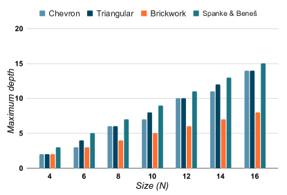
We first focus on the maximum depth, which quantifies the maximum number of switch points that a photon has to traverse. For the Triangular design in Sec. IV, the maximum depth is . For the Chevron design in Sec. V, the maximum depth is when is even, when is odd. The Brickwork design in Sec. VI reduces the maximum depth to . The maximum depth of the Triangular and Chevron designs is close to the optimal design for classical planar permutation networks, shown to be in [34]. The brickwork design on the other hand requires far fewer switch point traversals in the worst case scenario, reducing the overall loss in the switch.
In an ideal pairing mechanism, an arbitrary pair of input photons should traverse the same number of switch points in the same states. This is generally not true in real configurations, leading to an imbalance between the number of switch points that each photon of a pair passes through. In order to quantify this imbalance, we introduce the depth difference , defined intuitively as the difference between the maximum and the minimum depths of the switch. It is straightforward to see from Fig. 2 that the minimum depth for the Triangular design is 0. Therefore the , which is also the maximum depth.
For the Chevron design, the maximum depth depends on the parity of . When is odd, a photon traverses at most switch points, while its pairing partner needs to pass through at least switch points, giving . The same depth difference is obtained for the case when is even. In this case, the maximum and minimum depths are given by and , respectively. In the Brickwork design, the maximum depth is , while the minimum depth is , resulting .
| our designs | Spanke & Beneš [34] | Beneš [4] | Waksman [5] | |
| Planar/non-planar | planar | planar | non-planar | non-planar |
| No. of Switches | ||||
| Non-switching crosspoints | ||||
| No. of coupling & decoupling stages |
Out of the three proposed switches, the Brickwork design is the most balanced thanks to its lowest depth difference. This means that the photons traversing the switch experience comparable losses. The opposite is true for the Triangular design. Whether this is an undesirable effect ultimately depends on the network traffic. For quantum networks with fairly uniform traffic patterns, the Triangular design results in an uneven distribution of end-to-end Bell pair generation rates, leading to a decrease in the quality of service for certain connections. On the other hand, we can envision scenarios where this imbalance may be a welcome feature. The input ports with few switch points and their respective BSAs can be reserved for high-demand connections. For example, the optical switch may be a component of a quantum gateway connecting two independent networks. The low-loss input ports can be used for internetwork connections, while the more lossy input ports can be used for entanglement distribution within a single network.
VII-B Comparison with other designs
In this section, we compare the designs in terms of the number of switches with other related designs. Fig. 7 illustrates the maximum depth for the our proposed designs and those analyzed in [34]. Given that our switches are designed for paired-egress BSA pools, it is not surprising that the their maximum depth is always lower than the optimal full permutational switch of [34].
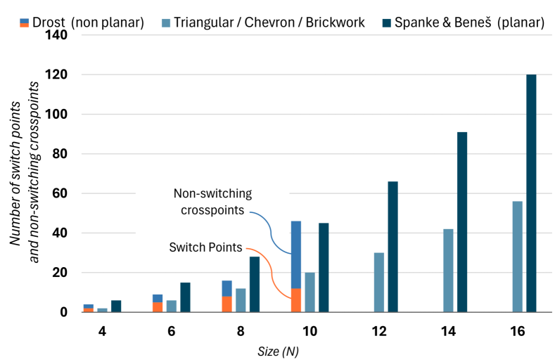
Fig. 8 shows the minimum number of required switch points in related planar and non-planar designs for up to 16 input ports. The focus of this paper has been planar designs suitable for chip fabrication, but of course non-planar designs can simply be “flattened” into planar form. In this case, we have to consider the fixed crosspoints, which can be viewed as planar switch points with permanent Cross states.
Drost et al.’s work proposing designs for small-scale non-planar switching networks is the work most comparable to our own, but does not address planar designs and does not include a scalable design [33]. Fig. 8 includes data on planarized Drost designs, counting switches and non-switching crosspoints up to 10 ports, the largest design they found. More detailed follow-on design work needs to consider the non-planar design and analyze the photon loss based on the number of interfaces required for coupling and decoupling of input photons toward switches.
Table I compares our proposed planar designs for paired egress to other scalable designs. To the best of our knowledge, no scalable structure for input pairing has been found before this work. Therefore we compare to some important full permutation switch networks. As the table shows, the key result of our paper is the reduction in switch points compared to Spanke and Beneš’s optimal planar design for full permutation switching networks [34].
VIII Conclusion
We have shown that for an switching network with paired-egress BSA Pools, the lower bound on the number of switching points in a planar architecture is . We proposed three rearrangeable non-blocking designs that saturate this lower bound, along with their corresponding efficient routing algorithms. Due to their recursive construction, our designs can be scaled to arbitrary size.
Our switch designs can be reversed in a straightforward manner. The BSAs can be replaced with EPPS nodes, and the routing algorithms then distribute the entangled photon pairs to the desired outputs. Therefore, our solution is directly applicable to the shared EPPS Pools switching problem considered in [33].
The shared BSA Pool architecture was recently used as an integral component in a proposal for distribution of remote entanglement between neutral ytterbium atoms coupled to optical cavities [48]. This demonstrates the relevance of optical switches with paired-egress BSA Pools, and the role they are expected to play in distributed quantum computing and quantum networking.
The performance of distributed systems crucially depends on how effectively we can harness the power of connected computers. This effectiveness largely relies on the performance of their network systems and architecture. Ideally, the network should always be capable of processing communication requests from computers; any delay waiting for network responses leads to decreased overall performance. Our rearrangeable non-blocking design ensures that the inputs and outputs of switches operate without stalling, achieving multiplexed parallel communication processing among different input-output pairs. Therefore, our optical switch designs prevent contention for communication from being a system-wide bottleneck. Thereby our work is essential for large-scale distributed quantum computers and the quantum Internet.
Acknowledgment
The authors would like to thank Takao Tomono, Rikizo Ikuta, and Alto Osada for their help and fruitful discussions.
References
- [1] C. Clos, “A study of non-blocking switching networks,” Bell System Technical Journal, vol. 32, no. 2, pp. 406–424, 1953, doi:10.1002/j.1538-7305.1953.tb01433.x.
- [2] D. C. Opferman and N. T. Tsao-Wu, “On a class of rearrangeable switching networks part i: Control algorithm,” The Bell System Technical Journal, vol. 50, no. 5, pp. 1579–1600, 1971, doi:10.1002/j.1538-7305.1971.tb02569.x.
- [3] V. E. Beneš, Mathematical theory of connecting networks and telephone traffic. Academic press, 1965, doi:10.2307/2343633.
- [4] V. E. Beneš, “Optimal rearrangeable multistage connecting networks,” The Bell System Technical Journal, vol. 43, no. 4, pp. 1641–1656, 1964, doi:10.1002/j.1538-7305.1964.tb04103.x.
- [5] A. Waksman, “A permutation network,” Journal of the ACM (JACM), vol. 15, no. 1, pp. 159–163, 1968, doi:10.1145/321439.321449.
- [6] W. C. Athas and C. L. Seitz, “Multicomputers: message-passing concurrent computers,” IEEE Computer, vol. 21, pp. 9–24, Aug. 1988, doi:10.1109/2.73.
- [7] W. J. Dally and B. Towles, Principles and Practices of Interconnection Networks. Elsevier, 2004.
- [8] D. D. Awschalom et al., “A roadmap for quantum interconnects,” Argonne National Laboratory (ANL), Argonne, IL (United States), Tech. Rep., 2022, doi:10.2172/1900586.
- [9] L. Jiang, J. M. Taylor, A. S. Sørensen, and M. D. Lukin, “Distributed quantum computation based on small quantum registers,” Phys. Rev. A, vol. 76, p. 062323, Dec 2007, doi:10.1103/PhysRevA.76.062323.
- [10] L. Jiang, J. M. Taylor, A. S. Sørensen, and M. D. Lukin, “Scalable quantum networks based on few-qubit registers,” International Journal of Quantum Information, vol. 8, no. 01n02, pp. 93–104, 2010, doi:10.1142/S0219749910006058.
- [11] J. Kim and C. Kim, “Integrated optical approach to trapped ion quantum computation,” QIC, vol. 9, no. 2, 2009.
- [12] J. Kim et al., “System design for large-scale ion trap quantum information processor,” QIC, vol. 5, no. 7, pp. 515–537, 2005, doi:10.26421/QIC5.7-1.
- [13] Y. L. Lim, S. D. Barrett, A. Beige, P. Kok, and L. C. Kwek, “Repeat-Until-Success quantum computing using stationary and flying qubits,” Physical Review Letters, vol. 95, no. 3, p. 30505, 2005, doi:10.1103/PhysRevA.73.012304.
- [14] C. Monroe et al., “Large-scale modular quantum-computer architecture with atomic memory and photonic interconnects,” Phys. Rev. A, vol. 89, p. 022317, Feb 2014, doi:10.1103/PhysRevA.89.022317.
- [15] N. H. Nickerson, Y. Li, and S. C. Benjamin, “Topological quantum computing with a very noisy network and local error rates approaching one percent,” Nature communications, vol. 4, p. 1756, 2013, doi:10.1038/ncomms2773.
- [16] D. K. L. Oi, S. J. Devitt, and L. C. L. Hollenberg, “Scalable error correction in distributed ion trap computers,” Physical Review A, vol. 74, p. 052313, 2006, doi:10.48550/arXiv.quant-ph/0606226.
- [17] R. Van Meter III, “Architecture of a quantum multicomputer optimized for Shor’s factoring algorithm,” Ph.D. dissertation, Keio University, 2006, available as arXiv:quant-ph/0607065. doi:10.48550/arXiv.quant-ph/0607065.
- [18] R. Van Meter and S. Devitt, “The path to scalable distributed quantum computing,” IEEE Computer, vol. 49, no. 9, pp. 31–42, Sep. 2016, doi:10.1109/MC.2016.291.
- [19] A. Yimsiriwattana and S. J. Lomonaco Jr, “Distributed quantum computing: A distributed shor algorithm,” in Quantum Information and Computation II, vol. 5436. SPIE, 2004, pp. 360–372, doi:10.1117/12.546504.
- [20] S. DiAdamo, M. Ghibaudi, and J. Cruise, “Distributed quantum computing and network control for accelerated VQE,” IEEE Transactions on Quantum Engineering, vol. 2, pp. 1–21, 2021, doi:10.1109/TQE.2021.3057908.
- [21] R. Satoh, M. Hajdušek, and R. Van Meter, “Federated graph state preparation on noisy, distributed quantum computers,” IPSJ Quantum Software SIG Technical Reports, vol. 2020-QS-1, p. 6, 2020.
- [22] R. Van Meter, K. Nemoto, W. Munro, and K. M. Itoh, “Distributed arithmetic on a quantum multicomputer,” ACM SIGARCH Computer Architecture News, vol. 34, no. 2, pp. 354–365, 2006, doi:10.48550/arXiv.quant-ph/0607160.
- [23] R. Van Meter, K. Nemoto, and W. Munro, “Communication links for distributed quantum computation,” IEEE Transactions on Computers, vol. 56, no. 12, pp. 1643–1653, 2007, doi:10.48550/arXiv.quant-ph/0701043.
- [24] M. Caleffi et al., “Distributed quantum computing: a survey,” arXiv preprint arXiv:2212.10609, 2022, doi:10.48550/arXiv.2212.10609.
- [25] S. Gauthier, G. Vardoyan, and S. Wehner, “An architecture for control of entanglement generation switches in quantum networks,” IEEE Transactions on Quantum Engineering, vol. 4, no. 01, pp. 1–17, 2023, doi:10.1109/TQE.2023.3320047.
- [26] M. Alshowkan et al., “Reconfigurable quantum local area network over deployed fiber,” PRX Quantum, vol. 2, p. 040304, Oct 2021, doi:10.1103/PRXQuantum.2.040304.
- [27] E. Bersin et al., “Development of a Boston-area 50-km fiber quantum network testbed,” Phys. Rev. Appl., vol. 21, p. 014024, Jan 2024, doi:10.1103/PhysRevApplied.21.014024.
- [28] W. Kozlowski et al., “Rfc 9340: Architectural principles for a quantum internet,” 2023, doi:10.17487/RFC9340.
- [29] M. Hajdušek and R. Van Meter, “Quantum communications,” arXiv preprint arXiv:2311.02367, 2023, doi:10.48550/arXiv.2311.02367.
- [30] S. Wehner, D. Elkouss, and R. Hanson, “Quantum internet: A vision for the road ahead,” Science, vol. 362, no. 6412, p. eaam9288, 2018, doi:10.1126/science.aam9288.
- [31] R. Van Meter et al., “A quantum internet architecture,” in 2022 IEEE International Conference on Quantum Computing and Engineering (QCE), 2022, pp. 341–352, doi:10.1109/QCE53715.2022.00055.
- [32] R. Van Meter, Quantum Networking. John Wiley & Sons, 2014, doi:10.1002/9781118648919.
- [33] R. J. Drost, T. J. Moore, and M. Brodsky, “Switching networks for pairwise-entanglement distribution,” Journal of Optical Communications and Networking, vol. 8, no. 5, pp. 331–342, 2016, doi:10.1364/JOCN.8.000331.
- [34] R. A. Spanke and V. Beneš, “N-stage planar optical permutation network,” Applied Optics, vol. 26, no. 7, pp. 1226–1229, 1987, doi:10.1364/AO.26.001226.
- [35] V. Krutyanskiy et al., “Entanglement of trapped-ion qubits separated by 230 meters,” Phys. Rev. Lett., vol. 130, p. 050803, Feb 2023, doi:10.1103/PhysRevLett.130.050803.
- [36] A. Crespi et al., “Integrated photonic quantum gates for polarization qubits,” Nature communications, vol. 2, no. 1, p. 566, 2011, doi:10.1038/ncomms1570.
- [37] G. Corrielli et al., “Rotated waveplates in integrated waveguide optics,” Nature communications, vol. 5, no. 1, p. 4249, 2014, doi:10.1038/ncomms5249.
- [38] X. Xu et al., “Self-calibrating programmable photonic integrated circuits,” Nature Photonics, vol. 16, no. 8, pp. 595–602, 2022, doi:10.1038/s41566-022-01020-z.
- [39] W. Bogaerts et al., “Programmable photonic circuits,” Nature, vol. 586, no. 7828, pp. 207–216, 2020, doi:10.1038/s41586-020-2764-0.
- [40] J. Wang, F. Sciarrino, A. Laing, and M. G. Thompson, “Integrated photonic quantum technologies,” Nature Photonics, vol. 14, no. 5, pp. 273–284, 2020, doi:10.1038/s41566-019-0532-1.
- [41] B. E. Saleh and M. C. Teich, Fundamentals of Photonics. John Wiley & Sons, 2019, doi:10.1002/0471213748.
- [42] J. Kim et al., “1100x1100 port MEMS-based optical crossconnect with 4-dB maximum loss,” IEEE Photonics Technology Letters, vol. 15, no. 11, pp. 1537–1539, 2003, doi:10.1109/LPT.2003.818653.
- [43] N. C. Harris et al., “Large-scale quantum photonic circuits in silicon,” Nanophotonics, vol. 5, no. 3, pp. 456–468, 2016, doi:10.1515/nanoph-2015-0146.
- [44] M. Lončar, D. Nedeljković, T. Doll, J. Vučković, A. Scherer, and T. P. Pearsall, “Waveguiding in planar photonic crystals,” Applied Physics Letters, vol. 77, no. 13, pp. 1937–1939, 2000, doi:10.1063/1.1311604.
- [45] J. L. O’Brien, A. Furusawa, and J. Vučković, “Photonic quantum technologies,” Nature photonics, vol. 3, no. 12, pp. 687–695, 2009, doi:10.48550/arXiv.1003.3928.
- [46] C. Taballione et al., “8 8 reconfigurable quantum photonic processor based on silicon nitride waveguides,” Optics express, vol. 27, no. 19, pp. 26 842–26 857, 2019, doi:10.1364/OE.27.026842.
- [47] A. Nesic et al., “Photonic-integrated circuits with non-planar topologies realized by 3d-printed waveguide overpasses,” Optics Express, vol. 27, no. 12, pp. 17 402–17 425, 2019, doi:10.1364/OE.27.017402.
- [48] Y. Li and J. Thompson, “High-rate and high-fidelity modular interconnects between neutral atom quantum processors,” arXiv preprint arXiv:2401.04075, 2024, doi:10.48550/arXiv.2401.04075.