2023
[1]\fnmDaniel \surAssumpcao\equalcontThese authors contributed equally to this work. [1]\fnmDylan \surRenaud\equalcontThese authors contributed equally to this work. [1]\fnmMarko \surLoncar
1]\orgdivJohn A. Paulson School of Engineering and Applied Sciences, \orgnameHarvard University, \orgaddress\cityCambridge, \postcode02138, \stateMA, \countryUnited States 2]\orgdivAWS Center for Quantum Networking, \orgaddress\cityBoston, \postcode02135, \stateMA, \countryUnited States 3]\orgnameDRS Daylight Solutions, \orgaddress\citySan Diego, \postcode16465, \stateCA, \countryUnited States
A Thin Film Lithium Niobate Near-Infrared Platform for Multiplexing Quantum Nodes
keywords:
Visible Wavelength, Lithium Niobate, Integrated PhotonicsPractical quantum networks will require quantum nodes consisting of many memory qubits. This in turn will increase the complexity of the photonic circuits needed to control each qubit and will require strategies to multiplex memories and overcome the inhomogeneous distribution of their transition frequencies. Integrated photonics operating at visible to near-infrared (VNIR) wavelength range, compatible with the transition frequencies of leading quantum memory systems, can provide solutions to these needs. In this work, we realize a VNIR thin-film lithium niobate (TFLN) integrated photonics platform with the key components to meet these requirements. These include low-loss couplers ( 1 dB/facet), switches ( 20 dB extinction), and high-bandwidth electro-optic modulators ( 50 GHz). With these devices we demonstrate high-efficiency and CW-compatible frequency shifting ( 50 efficiency at 15 GHz), as well as simultaneous laser amplitude and frequency control through a nested modulator structure. Finally, we highlight an architecture for multiplexing quantum memories using the demonstrated TFLN components, and outline how this platform can enable a 2-order of magnitude improvement in entanglement rates over single memory nodes. Our results demonstrate that TFLN can meet the necessary performance and scalability benchmarks to enable large-scale quantum nodes.
1 Introduction
The distribution of quantum entanglement across continental distances via quantum networks is an enabling technology for a variety of applications, including quantum key distribution, sensing, and distributed quantum computing Kimble2008 ; Wehner2018 . An important step towards this goal is generation of remote entanglement between spatially separated quantum memory nodes. Despite great experimental progress Covey2023 ; Hensen2015 ; Hermans2022 ; Leent2022 ; Delteil2016 ; Knaut2023 , the rate of entanglement generation across km scale distances has been limited to the sub-Hz regime. Transitioning these experiments from proof-of-concept demonstrations to practical networking technology requires increasing the number of qubits to 100s-1000s or even beyond. This would enable both increasing entanglement generation rates through multiplexing as well as the utilization of qubits as auxiliary memories for multi-qubit protocols such as entanglement distillation or entanglement swapping Wehner2018 ; Duan2001 ; Bennett1996 .
To effectively scale the number of qubits per node, however, several key technical innovations are necessary. First, the qubits and associated controls must be manufacturable in a scalable way. While solid-state qubits satisfy this criteria, their optical control currently requires bulky off-the-shelf lasers as well as acousto-optic and electro-optic modulators. Moreover, solid-state qubits, such as color centers, suffer from variations in their transition frequency which prevents entanglement generation between these qubits Evans2016 . Therefore, a method to efficiently frequency shift photons emitted by the qubits is required to overcome this inhomegenous broadening. Finally, the ability to connect any of the on-chip memories to a common optical channel (e.g. optical fiber) is essential to enable temporal multiplexing that can significantly increase the entanglement generation rate. This can be accomplished using a large on-chip switch network . All of these functionalities must be implemented with minimal additional insertion loss. This can be challenging since , the majority of quantum emitters have optical transitions in the visible and near-infrared regime (400 nm - 1000 nm) which is above the bandgap of traditional photonic integrated circuit (PIC) platforms such as indium phosphide or silicon Zeng2023 . On the other hand, silicon nitride does offer a suitable transparency window, but available modulation approaches based on the thermo-optic effect or the piezo-electric effect, are slow and cannot achieve 10s to 100s MHz switching speeds required for multiplexing Mohanty2020 ; Sacher2019 ; Dong2022 .
Recently thin-film lithium-niobate (TFLN) on insulator has emerged as a promising PIC platform due to its combination of large electro-optic (EO) coefficient, low optical losses, and large transparency window extending to 400 nm Zhang2023 ; Zhu2021 . High-performance visible systems have been fabricated on TFLN including low-loss passive devices and active modulators Desiatov2019 ; Renaud2023 ; Christen2022 ; Sund2023 ; Valdez2023 .
In this work we extend these results and demonstrate the key building blocks needed to scale quantum networking technology. We propose a TFLN photonic enabled architecture to realize a scalable quantum node, and demonstrate the necessary devices to realize this vision. This includes high-efficiency couplers with coupling efficiencies below 1 dB/facet, high-bandwidth phase modulators which we utilize to frequency shift a CW tone by up to 15 GHz with efficiencies beyond , and optical switches with high extinction ratio (20 dB) and suitable EO bandwidth for multiplexing. To both highlight the scalability of the platform and provide a compact solution for qubit optical control hardware, we also demonstrate a multi-component laser control unit PIC, which can be used to provide amplitude and frequency control of an input laser in our proposed architecture.
2 Results
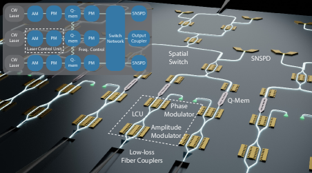
Our proposed TFLN architecture to realize a scalable quantum network node is depicted in Fig. 1. It consists of a combination of amplitude modulators (AM), frequency shifting via phase modulators (PM), switches, and high efficiency fiber-couplers all interfaced with a large array of quantum memory (QM) devices (see supplementary information for detailed discussion). These devices provide the necessary functionalities to effectively scale the optical control and multiplex the output of the QM modules. We note that although in our schematic the QMs are depicted as integrated within the PIC, this is not a requisite for our architecture. For example, the TFLN control PIC can be connected to QMs on a separate chip using low loss fiber couplers Zhang2023 ; Burek2017 , that we discuss next.
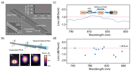
For high-fidelity and high-rate entanglement generation and distribution, minimizing insertion loss of all optical components, including the on/off-chip coupling losses, is paramount. Inspired by the ultra-low coupling efficiencies achieved using adiabatic tapered fiber-to-chip interfaces in diamond and silicon-nitride platforms, we develop an adiabatic fiber coupler in TFLN (Fig. 2) Burek2017 ; Zeng2023 ; Khan2020 ; Tiecke2015 . The primary challenge for low-loss adiabatic fiber couplers in TFLN is underlying oxide cladding that can support leaky modes. Therefore, to achieve efficient coupling between the TFLN and optical fiber, the TFLN waveguide must be suspended. We implement our design by first using a TFLN bilayer taper He2019 to adiabatically convert the rib waveguide mode to a ridge waveguide. Next, the ridge width is decreased to create an inverted taper (”lower taper”) which expands the mode (Fig. 2a) so that it can be coupled to a tapered optical fiber. A clamp is included at the end of the suspended lower taper to prevent collapsing of the device. A tapered optical fiber touches down on the TFLN lower taper, ensuring an efficient, adiabatic mode transfer between the fiber and TFLN waveguides. The geometry was optimized via finite-difference-time-domain (FDTD) simulations, with a peak simulated efficiency of 99 (Fig. 2a inset). The achievable efficiency in simulations is primarily limited by the lower tip dimension, which in our fabricated devices is nm. Fabricated devices (for details, see methods) were characterized and featured coupling losses as low as 0.9 dB/facet (81.2 efficiency), with optical bandwidths exceeding 100 nm. The discrepancy between simulated and measured losses is attributed to scattering at the bilayer taper rib-ridge mode conversion interface, shown in the inset of Fig. 2a. Still we emphasize that measured fiber-coupling values are state-of-the-art for TFLN couplers at visible to near-infrared wavelengths, and are comparable to the best demonstrated at telecom wavelengths as well Lomonte2021 ; Hu2021 .
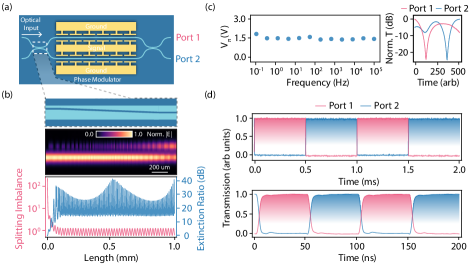
Spatial switches are required to route photons for both multiplexing and on-chip entanglement generation. We implement an EO switch using a Mach-Zehnder modulator (MZM) based design with 2x2 couplers at the input and output of the device (Fig. 3a). Adiabatic couplers are used for the 2x2 splitter to ensure fabrication robustness (Fig. 3b) (see supplementary information for additional design details) Cao2010 ; Yun2015 . We use numerical simulations to evaluate the splitting imbalance of the coupler, defined as the ratio of powers at the two output ports when coupler is excited using a single input port. We also evaluate the maximum extinction ratio achievable by a Mach Zehnder modulator utilizing two of these couplers due to the simulated splitting imbalance (Fig. 3b). Although some the splitting ratio and corresponding modulator extinction ratio still depends on the length of the coupler, likely due to partial coupling of the two waveguides on the imbalanced width side of the splitter, splitting imbalances are still close to 1 and extinction ratio of 15dB can still be achieved even in the worst case. This indicates tolerance to fabrication imperfections. Fabricated devices feature an on-chip loss of 0.4 dB per switch, which is limited by on-chip propagation losses (see supplementary information for supporting measurements). To control the switch, we employ capacitive lumped element electrodes (as opposed to traveling-wave designs discussed below) to limit power consumption. A half-wave voltage () of V is measured for a 5 mm modulator, with extinction ratios greater than 20dB on both ports (Fig. 3c). We note that the observed is flat as a function of frequency down to 0.1 Hz, which is important both for low frequency switching operation and achieving a stable modulator bias Holzgrafe2024 . We leverage this flat response to demonstrate switching between the two ports at kHz and MHz timescales, both of which are relevant for memory and photon operations, respectively, for typical solid-state emitters (Fig. 3d) Nguyen2019 ; Hensen2015 ; Lukin2020 ; Bradac2019 . Importantly, these capacitive electrodes do not dissipate significant power in the hold state , and only 100 for 10 MHz switching, (see supplementary information for details). This suggests that large switch networks can be created with minimal electrical overhead, making them suitable for multiplexing quantum memories even at cryogenic temperatures.
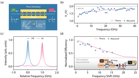
To overcome the inhomogeneous distribution of QM optical transitions, our platform incorporates optical frequency-shifting capabilities. We choose to utilize a serrodyne-based frequency approach whereby a linear advance in phase is emulated using a sawtooth wave with an amplitude of applied to the phase modulator. This approach in principle can enable frequency shifts with unity efficiency and functions irrespective of the temporal shape of the input light (Fig. 4a) Holland2021 ; Johnson2010 ; Houtz2009 ; Poberezhskiy2005 ; Sinclair2014 ; Saglamyurek2014 (see supplementary information for details). The latter is especially important, as quantum memories can possess narrow transitions with correspondingly long photon lifetimes (ns or longer). The challenge with serrodyning is that due to the high-bandwidth nature of an electrical sawtooth wave, a large analog bandwidth is required from both the modulator and the control electronics.
To realize this, we utilize a segmented-electrode PM Kharel2021 . This design increases the microwave index of the electrode, allowing us to achieve microwave-optical velocity matching with a smaller impedance penalty than achieved previously (see supplementary information for supporting data and simulations). In addition, this electrode design exhibits decreased Ohmic losses due to the breaking of the current path on the inner portion of the electrode Kharel2021 ; Ding2014 ; Shin2011 . With this design, we realize high-bandwidth phase modulators with estimated 3-dB bandwidths of 55 GHz ( 100 GHz) with respect to 2GHz ( 5 GHz) response, which is a considerable enhancement over previously achieved results (35 GHz with respect to 3 GHz response) Renaud2023 (Fig. 4b). We estimate an on-chip optical loss of 0.7 dB for a 1-cm device (see supplementary information for supporting measurements).
Utilizing this modulator we perform a proof-of-principle serrodyne frequency shifting demonstration. We apply a sawtooth electrical waveform onto the phase modulator using a fast arbitrary waveform generator (AWG) and radio-frequency (RF) amplifier. The transmitted light is measured in the frequency domain by a scanning Fabry-Perot (FP) cavity. We observe frequency shifts of 1 GHz with high () efficiencies (Fig. 4c). To understand the limits of this serrodyning technique, we sweep the shift frequency and measure the efficiency (Fig. 4d). We find that there is an efficiency roll-off at higher frequencies attributed to the limited analog electrical bandwidth of 35 GHz amplifier used in our experiments. A model considering the finite bandwidth of the amplifier accurately reproduces our results, as shown in Fig. 4d (see supplementary information for model information). Despite this, we are still able to achieve shifts up to 15 GHz with shift efficiencies beyond 50. Notably, this is sufficient to overcome the inhomogeneous distribution of various diamond QMs Evans2016 ; Machielse2019 , and a significant improvement over previous demonstrations which were limited to 5 GHz Sinclair2014 ; Saglamyurek2014 . Going forward, we note that using state-of-the-art high-bandwidth electronics, even larger shifts can be achieved using the same modulator (see supplementary information for details) Chen2017 . This demonstrates the utility of our PMs coupled with serrodyning technique to achieve ultra-large frequency shifts, with small added loss, for overcoming the inhomogeneous distribution of solid state QMs.
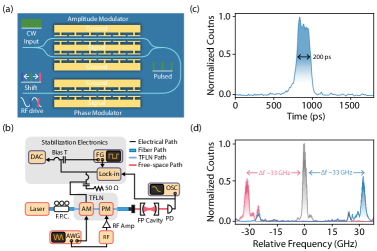
To control QMs, CW and pulsed laser signals are needed. Inhomogeneous broadening of QMs, however, requires laser light of different wavelengths and pulse durations. One approach would be to utilize integrated photonic lasers with emission wavelengths tuned to particular QMs of interest Tran2019 ; amirlaser . This approach does not scale well, as it would require an individual laser per quantum memory. QM optical control typically requires low laser linewidth for high-fidelity operations (kHz) and low optical power. As laser optical power and laser linewidth are inversely correlated Henry1982 ; Coldren2012 , it is most efficient to have one integrated, higher power and low linewidth laser driving multiple QMs. This can be achieved using a laser control unit (LCU, Fig. 1) consisting of an AM followed by a PM (Fig. 5a) for each QM. This combination not only enables the amplitude and frequency shaping of input CW light to generate optical control pulses to interface with QMs, but also shows the ability of our platform to support complex PICs containing multiple nested devices.
To illustrate the capabilities of the LCU, we implement a pulse shaping and shearing protocol to create a train of short pulses, and subsequently shift their central frequency. The AM is used to carve short pulses, which are then sent to a PM and temporally aligned with the linear rising/falling region of an applied sinusoidal tone (Fig. 5a). This introduces a frequency shift, and is commonly referred to as EO shearing Johnson1988 ; Wright2017 ; Zhu2022 . We have previously demonstrated state-of-the-art EO shearing with TFLN modulators, measuring maximum shifts of over 7 times the pulse linewidth Renaud2023 . However, in that work the pulse generation was done with a separate commercial AM. As the LCU contains both an AM and PM, we are able to perform amplitude and frequency shaping operations within the same PIC.
We utilize a electronic setup similar to our previous demonstration, with both the sinusoidal tone and the electrical pulses originating from a common AWG. The sinusoidal tone and RF pulses are applied to the PM and AM, respectively (Fig. 5b). We bias the amplitude modulator at the null point for pulse generation using a quasi-DC electro-optic bias whereby a feedback loop is applied to the low-frequency electrical bias of the modulator loop to overcome the DC bias drift prevalent in TFLN modulators Sosunov2021 ; Holzgrafe2024 . By avoiding biasing using heaters, we ensure our devices can be used in cryogenic settings (see supplementary information for additional details).
Short (200 ps) optical pulses are generated by the AM directly driven by the AWG (Fig. 5c), which is faster than typically required for quantum optical control pulses. We then apply a 250 MHz sinusoidal tone to the PM and measure the resultant frequency spectrum via a FP cavity (Fig. 5d). We find that we can deterministically shift our optical pulses by GHz. This corresponds to a drive amplitude of 40 and a shift of over 16 times the linewidth (see supplementary information for details). This large shift is sufficient to cover the inhomogeneous distribution of a variety of different emitters, providing a method for creating optical pulses to address different emitters, all while being seeded by a single laser. We observe some distortion is induced via shearing, as seen in the spectrum of the sheared transmission spectra. We hypothesize that this distortion is due to the inherent nonlinearity of the sinusoidal drive signal used in our experiment (see supplementary information for details on the model). We believe that LCU will be crucial to limit the complexity of optical control while scaling up the number of qubits per node. Through direct integration of the laser within the PIC, its scalability can be enhanced even further amirlaser . Beyond this, these findings demonstrate the ability to create complex, multi-element PICs with our platform.
3 Discussion
In this work we have demonstrated the necessary ingredients to create PICs for multiplexing quantum network nodes, including state-of-the-art modulators, switches, and high efficiency couplers. Using this platform we have shown proof of principle demonstrations of its utility, including frequency shifting a CW tone beyond 15 GHz with efficiencies above 50 and creating multi-element PICs to provide amplitude and frequency control of optical pulses for simplifying optical control complexity at scale.
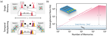
To contextualize the potential of this platform, we compute the benefits of temporal multiplexing using the TFLN-based architecture in Fig. 1 and our demonstrated device performance. We consider the model of two quantum nodes separated by a distance , where each node probabilistically generates a flying photon entangled with the local spin memory and sent to a central station where a detection of one of the photons heralds entanglement (see supplementary information for details) (Fig. 6). Although this architecture is largely quantum memory agnostic, for discussion purposes we focus on solid-state defects in diamond, and specifically the silicon vacancy center in diamond, due to their excellent optical and spin properties and ability to be fabricated at scale Evans2016 ; Tchernij2017 ; Lukin2020 ; Doherty2013 ; Bhaskar2020 . We consider two cases. The first is where only a single memory exists at each quantum node, and each node must wait the classical signaling time () between each entanglement attempt, limiting the repetition rate. The second case is where each quantum node has multiple memories which can be temporally interleaved via our TFLN PIC. This allows a significant increase in the repetition rate limited by the number of memories at each node and ultimately by the photon length,at the cost of additional losses from the TFLN PIC including coupling losses, frequency shifting losses, and device losses. We compute the achievable entanglement rates across a 20km channel for these two cases utilizing a silicon-vacancy center in diamond based quantum memory. In the temporal multiplexing case we incorporate the estimated losses of the PIC including both individual device loss and off-chip coupling losses (see supplementary information for full model details). Despite the additional overhead of the TFLN PIC, we estimate the advantage of temporal multiplexing will lead to an enhanced entanglement rate with even a modest number of memories ( 10) with an over 100x increase in rate achievable through saturation of the channel temporally (requiring memories) (Fig 6b). Through additional wavelength division multiplexing (WDM) using current telecom WDM technology, we estimate MHz entanglement rates can be achieved across the 20 km distance. This therefore demonstrates our platform achieves the necessary performance metrics and scalability to enable multiplexing and maximize quantum network performance.
Using this platform, future work will focus on increasing the complexity of visible TFLN PICs through increasing the number of elements and integrating with quantum memory systems to demonstrate the advantage of scalability. Moreover, due to the state-of-the-art performance of these devices, this platform can be applied to other quantum technology applications, such as control of atomic platforms, and even classical applications such as AR/VR, sensing, or communications operating in the visible region.
4 Methods
4.1 Device fabrication
All TFLN devices were realized on thin film wafers from NanoLN (X-cut, 300 nm LN/7 m SiO2/500 m Si). Integrated photonic devices are fabricated by first patterning waveguide layers using electron-beam lithography (HSQ, Elionix ELS-F125), and etching 180 nm using reactive ion etching (Ar+). This is then followed by re-deposition cleaning (RCA SC-1) and a high-temperature anneal (520 C). For fabrication details please see Ref Renaud2023 .
4.2 Modulator Measurements
For low frequency measurements, a variable frequency function generator produces a triangular waveform that is directed to the MZM electrodes using a 50 ground-signal-ground probe (40A-GSG-100-F). A CW laser () is coupled to the modulator and out-coupled to an avalanche photodetector (APD410A). The detector output is monitored on an electronic oscilloscope, from which the is extracted.
For high frequency measurements, a sinusoidal RF tone is applied at varying frequencies and the resulting optical spectrum is measured. The optical frequency spectrum of an MZM given an input CW optical carrier frequency of , an applied RF tone at frequency and amplitude , and internal phase between the arms of is given by:
| (1) |
where is an integer of the harmonic of the drive frequency Shi2003 .
The frequency spectrum is measured using a home-built Fabry-Perot cavity (linewidth = 200 MHz) and fit to 1.
For loss measurements, propagation loss was assumed to be the dominant loss, which was extracted via cutback measurements to be 0.7 dB/cm Renaud2023 .
4.3 Serrodyne Demonstration
Sawtooth electrical waveforms were generated using a fast arbitrary waveform generator (92 GSa, Keysight) and amplified via a high-bandwidth high-power amplifier. Pre-compensation is applied by the AWG to compensate for frequency-dependent loss induced distortions from both the cables, and the amplifier itself. The frequency spectrum of light transmitted through the modulator was measured via a scanning Fabry-Perot cavity. To compute the shift efficiency, the frequency spectrum of light transmitted through the modulator was measured with and without the applied sawtooth in quick succession to limit any setup drifts. The ratio of power in the shifted sideband to the initial unperturbed power was taken as the efficiency.
4.4 Shearing Demonstration
To bias the amplitude modulator at the null point, a dither-based feedback was used. A small sinusoidal frequency at a low frequency (1 kHz) was combined with a DC offset via a bias tee and then applied to the amplitude modulator via a second bias tee. The transmitted light was then detected on a photodetector and the voltage output routed to a lock in amplifier to demodulate the dither signal and provide an error value. A software based PID loop was then used to feedback the DC bias on this error value and ensure the amplitude modulator was locked to the null point.
With the amplitude modulator biased at the null point, short electrical pulses were applied to the amplitude modulator to generate the optical pulses while a sinusoidal tone was applied to the phase modulator. Both were generated by the same AWG (Tektronix 70000). For the shearing demonstration, an optical pulse length of 400 ps was used. Although shorter pulses could be generated, the total frequency shift with these pulses would be larger than the free-spectral range of the FP cavity (70 GHz) leading to aliasing artifacts.
We also note that the phase modulator was operated in lumped element configuration with no termination. This was possible due to the electrical narrowband nature of shearing.
4.5 Adiabatic Coupler Design
We simulate this coupler using an eigenmode expansion (EME) solver (Lumerical) to calculate the splitting ratio and the correspond extinction ratio of the modulator as a function of length. We find that the coupler reaches the adiabatic condition at a length of 100 µm. While there is still a variation of splitting ratio and extinction for longer lengths, the worst case extinction ratio is still 15 dB, thus ensuring fabrication robustness. The simulated insertion loss is negligible ( dB).
Supplementary information See supplementary document for supporting content.
Declarations
Acknowledgements This work was supported in part by AFOSR FA9550-20-1-0105 (M.L., D. R.), AFOSR FA9550-19-1-0376 (M.L., A. S. A), ARO MURI W911NF1810432 (D. R. D. B., M.L.), NSF EEC-1941583 (M.L. D. A. K. P., C. X.), NSF OMA-2137723 (M.L., C. X.), OMA-2138068 (M.L., M. Y.), AWS Center for Quantum Networking’s research alliance with the Harvard Quantum Initiative (M.L. D. A. D. R., C. X.), Ford Foundation Fellowship, (D.R.), and NSF GRFP No. DGE1745303 (D.R., D.A.). Device fabrication was performed at the Center for Nanoscale Systems (CNS), a member of the National Nanotechnology Coordinated Infrastructure Network (NNCI), which is supported by the National Science Foundation under NSF Grant No. 1541959. \bmheadCompeting interests M.L. is involved in developing lithium niobate technologies at HyperLight Corporation. The remaining authors declare no competing interests \bmheadAvailability of data and materials The data presented in this study is available from the corresponding authors upon request. \bmheadAuthors’ contributions These authors contributed equally: Daniel Assumpcao and Dylan Renaud.
References
- \bibcommenthead
- (1) Kimble, H. J. The quantum internet (2008).
- (2) Wehner, S., Elkouss, D. & Hanson, R. Quantum internet: A vision for the road ahead (2018).
- (3) Covey, J. P., Weinfurter, H. & Bernien, H. Quantum networks with neutral atom processing nodes (2023).
- (4) Hensen, B. et al. Loophole-free bell inequality violation using electron spins separated by 1.3 kilometres. Nature 526 (2015). 10.1038/nature15759 .
- (5) Hermans, S. L. et al. Qubit teleportation between non-neighbouring nodes in a quantum network. Nature 605 (2022). 10.1038/s41586-022-04697-y .
- (6) van Leent, T. et al. Entangling single atoms over 33 km telecom fibre. Nature 607 (2022). 10.1038/s41586-022-04764-4 .
- (7) Delteil, A. et al. Generation of heralded entanglement between distant hole spins. Nature Physics 12 (2016). 10.1038/nphys3605 .
- (8) Knaut, C. M. et al. Entanglement of nanophotonic quantum memory nodes in a telecommunication network (2023) .
- (9) Duan, L. M., Lukin, M. D., Cirac, J. I. & Zoller, P. Long-distance quantum communication with atomic ensembles and linear optics. Nature 414 (2001). 10.1038/35106500 .
- (10) Bennett, C. H. et al. Purification of noisy entanglement and faithful teleportation via noisy channels. Physical Review Letters 76 (1996). 10.1103/PhysRevLett.76.722 .
- (11) Evans, R. E., Sipahigil, A., Sukachev, D. D., Zibrov, A. S. & Lukin, M. D. Narrow-linewidth homogeneous optical emitters in diamond nanostructures via silicon ion implantation. Physical Review Applied 5, 044010 (2016). 10.1103/PhysRevApplied.5.044010 .
- (12) Zeng, B. et al. Cryogenic packaging of nanophotonic devices with a low coupling loss ¡ 1 db. Applied Physics Letters 123, 161106 (2023). URL https://doi.org/10.1063/5.0170324. 10.1063/5.0170324 .
- (13) Mohanty, A. et al. Reconfigurable nanophotonic silicon probes for sub-millisecond deep-brain optical stimulation. Nature Biomedical Engineering 4 (2020). 10.1038/s41551-020-0516-y .
- (14) Sacher, W. D. et al. Visible-light silicon nitride waveguide devices and implantable neurophotonic probes on thinned 200 mm silicon wafers. Optics Express 27, 37400 (2019). 10.1364/OE.27.037400 .
- (15) Dong, M. et al. High-speed programmable photonic circuits in a cryogenically compatible, visible–near-infrared 200 mm cmos architecture. Nature Photonics 16, 59–65 (2022). 10.1038/s41566-021-00903-x .
- (16) Zhang, C. et al. Integrated photonics beyond communications. Applied Physics Letters 123, 230501 (2023). URL https://doi.org/10.1063/5.0184677. 10.1063/5.0184677 .
- (17) Zhu, D. et al. Integrated photonics on thin-film lithium niobate. Advances in Optics and Photonics 13 (2021). 10.1364/aop.411024 .
- (18) Desiatov, B., Shams-Ansari, A., Zhang, M., Wang, C. & Lončar, M. Ultra-low-loss integrated visible photonics using thin-film lithium niobate. Optica 6 (2019). 10.1364/optica.6.000380 .
- (19) Renaud, D. et al. Sub-1 volt and high-bandwidth visible to near-infrared electro-optic modulators. Nature Communications 14 (2023). 10.1038/s41467-023-36870-w .
- (20) Christen, I. et al. An integrated photonic engine for programmable atomic control (2022) .
- (21) Sund, P. I. et al. High-speed thin-film lithium niobate quantum processor driven by a solid-state quantum emitter. Science Advances 9 (2023). 10.1126/sciadv.adg7268 .
- (22) Valdez, F., Mere, V. & Mookherjea, S. 100 ghz bandwidth, 1 volt integrated electro-optic mach–zehnder modulator at near-ir wavelengths. Optica 10 (2023). 10.1364/optica.484549 .
- (23) Burek, M. J. et al. Fiber-coupled diamond quantum nanophotonic interface. Physical Review Applied 8 (2017). 10.1103/PhysRevApplied.8.024026 .
- (24) Khan, S. et al. Low-loss, high-bandwidth fiber-to-chip coupling using capped adiabatic tapered fibers. APL Photonics 5 (2020). 10.1063/1.5145105 .
- (25) Tiecke, T. G. et al. Efficient fiber-optical interface for nanophotonic devices. Optica 2 (2015). 10.1364/optica.2.000070 .
- (26) He, L. et al. Low-loss fiber-to-chip interface for lithium niobate photonic integrated circuits. Optics Letters 44 (2019). 10.1364/ol.44.002314 .
- (27) Lomonte, E., Lenzini, F. & Pernice, W. H. P. Efficient self-imaging grating couplers on a lithium-niobate-on-insulator platform at near-visible and telecom wavelengths. Optics Express 29 (2021). 10.1364/oe.428138 .
- (28) Hu, C. et al. High-efficient coupler for thin-film lithium niobate waveguide devices. Optics Express 29 (2021). 10.1364/oe.416492 .
- (29) Cao, L., Elshaari, A., Aboketaf, A. & Preble, S. Adiabatic couplers in soi waveguides (2010).
- (30) Yun, H. et al. 2x2 broadband adiabatic 3-db couplers on soi strip waveguides for te and tm modes (2015).
- (31) Holzgrafe, J. et al. Relaxation of the electro-optic response in thin-film lithium niobate modulators. Opt. Express 32, 3619–3631 (2024). URL https://opg.optica.org/oe/abstract.cfm?URI=oe-32-3-3619. 10.1364/OE.507536 .
- (32) Nguyen, C. T. et al. An integrated nanophotonic quantum register based on silicon-vacancy spins in diamond. Physical Review B 100, 165428 (2019). 10.1103/PhysRevB.100.165428 .
- (33) Lukin, D. M., Guidry, M. A. & Vučković, J. Integrated quantum photonics with silicon carbide: Challenges and prospects. PRX Quantum 1 (2020). 10.1103/PRXQuantum.1.020102 .
- (34) Bradac, C., Gao, W., Forneris, J., Trusheim, M. E. & Aharonovich, I. Quantum nanophotonics with group iv defects in diamond. Nature Communications 10, 5625 (2019). 10.1038/s41467-019-13332-w .
- (35) Holland, C. M., Lu, Y. & Cheuk, L. W. Synthesizing optical spectra using computer-generated holography techniques. New Journal of Physics 23 (2021). 10.1088/1367-2630/abe973 .
- (36) Johnson, D. M. S., Hogan, J. M., w. Chiow, S. & Kasevich, M. A. Broadband optical serrodyne frequency shifting. Optics Letters 35 (2010). 10.1364/ol.35.000745 .
- (37) Houtz, R., Chan, C. & Müller, H. Wideband, efficient optical serrodyne frequency shifting with a phase modulator and a nonlinear transmission line. Optics Express 17 (2009). 10.1364/oe.17.019235 .
- (38) Poberezhskiy, I. Y., Bortnik, B., Chou, J., Jalali, B. & Fetterman, H. R. Serrodyne frequency translation of continuous optical signals using ultrawide-band electrical sawtooth waveforms. IEEE Journal of Quantum Electronics 41 (2005). 10.1109/JQE.2005.858467 .
- (39) Sinclair, N. et al. Spectral multiplexing for scalable quantum photonics using an atomic frequency comb quantum memory and feed-forward control. Physical Review Letters 113 (2014). 10.1103/PhysRevLett.113.053603 .
- (40) Saglamyurek, E. et al. An integrated processor for photonic quantum states using a broadband light-matter interface. New Journal of Physics 16 (2014). 10.1088/1367-2630/16/6/065019 .
- (41) Kharel, P., Reimer, C., Luke, K., He, L. & Zhang, M. Breaking voltage–bandwidth limits in integrated lithium niobate modulators using micro-structured electrodes. Optica 8 (2021). 10.1364/optica.416155 .
- (42) Ding, R. et al. High-speed silicon modulator with slow-wave electrodes and fully independent differential drive. Journal of Lightwave Technology 32 (2014). 10.1109/JLT.2014.2323954 .
- (43) Shin, J., Sakamoto, S. R. & Dagli, N. Conductor loss of capacitively loaded slow wave electrodes for high-speed photonic devices. Journal of Lightwave Technology 29 (2011). 10.1109/JLT.2010.2091624 .
- (44) Machielse, B. et al. Quantum interference of electromechanically stabilized emitters in nanophotonic devices. Physical Review X 9, 031022 (2019). 10.1103/PhysRevX.9.031022 .
- (45) Chen, X. et al. All-electronic 100-ghz bandwidth digital-to-analog converter generating pam signals up to 190 gbaud. Journal of Lightwave Technology 35 (2017). 10.1109/JLT.2016.2614126 .
- (46) Tran, M. A., Huang, D. & Bowers, J. E. Tutorial on narrow linewidth tunable semiconductor lasers using si/iii-v heterogeneous integration. APL Photonics 4, 111101 (2019). URL https://doi.org/10.1063/1.5124254. 10.1063/1.5124254 .
- (47) Shams-Ansari, A. et al. Electrically pumped laser transmitter integrated on thin-film lithium niobate. Optica 9, 408–411 (2022). URL https://opg.optica.org/optica/abstract.cfm?URI=optica-9-4-408. 10.1364/OPTICA.448617 .
- (48) Henry, C. H. Theory of the linewidth of semiconductor lasers. IEEE Journal of Quantum Electronics 18 (1982). 10.1109/JQE.1982.1071522 .
- (49) Coldren, L. A., Corzine, S. W. & Mašanović, M. L. Diode Lasers and Photonic Integrated Circuits (2012).
- (50) Johnson, L. M. & Cox, C. H. Serrodyne optical frequency translation with high sideband suppression. Journal of Lightwave Technology 6 (1988). 10.1109/50.3974 .
- (51) Wright, L. J., Karpiński, M., Söller, C. & Smith, B. J. Spectral shearing of quantum light pulses by electro-optic phase modulation. Physical Review Letters 118, 023601 (2017). URL https://journals.aps.org/prl/abstract/10.1103/PhysRevLett.118.023601. 10.1103/PHYSREVLETT.118.023601/FIGURES/3/MEDIUM .
- (52) Zhu, D. et al. Spectral control of nonclassical light pulses using an integrated thin-film lithium niobate modulator. Light: Science and Applications 11 (2022). 10.1038/s41377-022-01029-7 .
- (53) Sosunov, A., Ponomarev, R., Zhuravlev, A., Mushinsky, S. & Kuneva, M. Reduction in dc-drift in linbo3-based electro-optical modulator. Photonics 8 (2021). 10.3390/photonics8120571 .
- (54) Tchernij, S. D. et al. Single-photon-emitting optical centers in diamond fabricated upon sn implantation. ACS Photonics 4 (2017). 10.1021/acsphotonics.7b00904 .
- (55) Doherty, M. W. et al. The nitrogen-vacancy colour centre in diamond (2013).
- (56) Bhaskar, M. K. et al. Experimental demonstration of memory-enhanced quantum communication. Nature 580 (2020). 10.1038/s41586-020-2103-5 .
- (57) Shi, Y., Yan, L. & Willner, A. E. High-speed electrooptic modulator characterization using optical spectrum analysis. Journal of Lightwave Technology 21 (2003). 10.1109/JLT.2003.818162 .