Reconstructed Electronic Structure in 2D vdW 1T-Ta for Quantum Sensing and Information Science
Abstract
Transition metal dichalcogenides (TMDs) are a class of two-dimensional (2D) layered materials that exhibit a diverse range of electronic structures, including charge density waves (CDWs) that can lead to insulating, semiconducting, metallic, and even superconducting phases. While the formation of CDWs in these systems has been recognized in early research [Phys. Rev. Lett. 129, 156401 (2022); Nat. Phys. 11, 328 (2015)], the underlying mechanisms driving the commensurate CDW (CCDW) phase remain largely unexplored. CCDWs typically originate from factors such as perfect Fermi surface nesting and/or electron-phonon coupling, causing the divergence of the chiral electronic structure. However, in the case of layered 2D TMD materials with CCDW phases, the significance of reconstructed electronic structures resulting from periodic lattice distortions (PLD) and photoemission matrix element effects in the CCDW instability needs to be visualized. This study focuses on computationally accessible CCDW phases in 1T-Ta, a prototypical TMD with a rich CDW phase diagram, aiming to understand the origins of CCDW phases. The insights gained from this investigation have the potential to advance the application of 2D materials in next-generation electronics, quantum sensing and information science.
keywords:
American Chemical Society, LaTeXIntroduction- Transition metal dichalcogenides (TMDs), a class of two-dimensional (2D) layered materials, possess have a range of electronic properties from insulating to semiconducting, metallic and even superconducting 1, 2, 3. It is pretty interesting to understand the driving mechanism behind the formation of the charge density waves (CDWs) in these systems, which is still unclear to address 4, 5. In general understanding, it is expected that perfection in Fermi-surface nesting (FSN) cause divergence in the electronic susceptibility. This process may cause the existence of CDW phases in this system. Meanwhile, scattering behaviour affect the atomic coherence and diminish this coherency when this material goes to a correlated electron state and vice versa. Thus, it is absolutely needed to persist such correlated electronic state in system to achieve long term CDW phase stability, where large and sharp interfaces in materials support this feature 6, 7. Considering these facts, 2D materials possess atomically large and sharp interfaces helping to hold robustly the correlated states over long distances with reduced scattering 8. Moreover, the graphene family and related 2D heterostructures support the observation of strong coupling effects (i.e. superconductivity, magnetism and spin-orbit coupling) at low dimensional length scale 9, 10.
Here, 1T-Ta is a TMD compound that exhibits a rich variety of CDW phases. The CDW in 1T-Ta is known to undergo several structural transitions, leading to the formation of commensurate CDW (CCDW) states. The understanding of the electronic structure and photoemission matrix element effects in these CDW phases is crucial for unraveling their complex behavior. However, there is increasing high questions raised to understand purely the FSN effect and electronic origins of the instability due to the CDW phase in layered quasi 2D CDW materials. In this line, first-principles reports on layered CDW materials (such as 1T-Ta, 1T-Ta, and 2H-Nb) show correlation-less between CDW ordering vector and strong nesting vectors that supports the role of electron-phonon interactions in the CDW formation. Meanwhile, the CDW phase can be extensively investigated as a another many-body quantum state due to electron-electron correlations 11, like on-site Coulomb repulsion and anti-ferromagnetic short-range spin-exchange interactions, predicted in various correlated insulators and unconventional superconductors 12. Previously, there is an instance of CDW phases observed in 2D TMDs 13, 14. It is challenging to study the chiral effect between normal and CDW phase of the same material including the role of scattering surfaces. Present work is considered for the 1T-Ta as a prototypical TMD having rich CDWs phase diagram 15. Using first-principles calculations, FSN effect, van Hove singularities and electron-phonon coupling are examined on the structural and electronic properties of the system 1, 16, 17. We further simulate the photoemission electronic spectra to understand the matrix element effects on the system.
Reconstructed Electronic Structure in 1T-Ta: The electronic structure of 1T-Ta is significantly modified in the presence of CDW phases. Several experimental techniques, such as angle-resolved photoemission spectroscopy (ARPES), scanning tunneling microscopy/spectroscopy (STM/STS), and X-ray scattering, have been employed to probe the electronic structure. ARPES measurements revealed the formation of an energy gap in the CDW state, indicating the opening of a partial band gap due to the reconstruction of the electronic structure 18. The band dispersion and the Fermi surface topology were found to be strongly modified in the CDW phase. STM/STS studies provided further insights into the CDW-induced electronic reconstruction and the emergence of localized states within the gap 19.
In this present work, we explore the FSN and CDW phase of the electronic structure in 1T-Ta within the framework of ab initio DFT calculations. We show importance of considering matrix elements as constant quantity, which is similar to treat free electrons. The present results of 1T-Ta system highlight the role of matrix elements inclusion in mapping the true instabilities of the material supporting with Wannier90 calculations. We realize that soft phonon modes give rise to instability and the system enters into a CCDW phase at distortions. Meanwhile, the inter-link among the electronic and lattice distortions checks further studies to realize the mediated interaction of the matrix elements. Thus, it shows that there is still a plenty of platform available to enlighten the era of rich physics.
Methodology Set-ups- The full cell geometry optimization and electronic structure calculations of the 1T-Ta system are performed using density functional theory (DFT) simulations. Here, projector augmented wave (PAW) 20, 21 formalism is considered during calculations with the Quantum ESPRESSO Package 22, 23, 24, 25. The Perdew-Burke-Ernzerhof (PBE) generalized-gradient approximation (GGA), specially for solids (PBESol) 26 is generally used to describe the exchange and correlation functional. The CDW structures are constructed in a supercell of the 1T-Ta starting from the experimental periodic lattice distortion (PLD) positions of atoms taken from Ref. 27. A 20 vacuum gap is included out-of-plane along c axis to avoid periodic image interaction. Here, full cell volume relaxation is performed with Methfessel-Paxton smearing () of 0.2 eV for all sets of calculations. All the geometric structures are fully relaxed until the force and energy tolerance convergence on each atom become 0.002 eV/ and eV, respectively. A set of K-point mesh is chosen to appropriately sample the Brillouin zone with respect to the primitive cell for the computation of the structure relaxations and the self consistent electronic densities and a denser, mesh for the computation of the densities of states. We set 580 eV as the cutoff energy and rev-vdW-DF2 28, 29 vdW correction for the calculations. The atoms in the CDW phase are fully relaxed while the lattice parameters are fixed at the values of the pristine phase. The tetrahedron method is employed in calculating the density of states and total energy. The phonon dispersion is calculated by using the finite displacement method using the PHONOPY code 30. Hamiltonian of tight-binding basis is used for FSN, photo-emmision matrix element properties based on the maximally localized Wannier functions (MLWFs) of WANNIER90 package 31. Moreover, simulate angle-resolved photoemission matrix elements are compared together to check the compatibility 32.
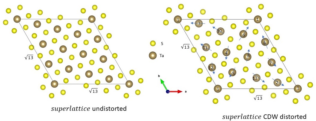
Tight-binding model calculations- We follow tight-binding model to present the reconstructed electronic structures of the 1T-Ta system with commensurate CDW locked in star-of-David cluster form. This model uses qualitatively the primary results of band structures in normal and CCDW phases. The Hamiltonian is formed by the Slater-Koster (SK) method 33. We considered , , and orbitals of Ta atoms as the basis due to their dominant band structure near Fermi level () during the calculations 34. It is noticed that in-plane displacements of Ta atoms are generally twice larger than the out-of-plane displacements of S atoms, while the system enters CCDW phase 35. In case of high temperature normal phase calculations, one Ta atom is present with two S atoms in the unit cell having a 6*6 square matrix, whereas 13 Ta atoms and 26 S atoms are present in the superlattice unit cell of the CCDW phase having matrix (in case of spin orbit coupling). We can obtain the energy eigen values along with the band dispersions and constant-energy contours by diagonalizing the Hamiltonian matrix. We obtain the tight-binding model parameters from literature 34 and use in this calculations. We scale the SK hopping integrals with respect to the inverse cubic Ta-Ta distance to fit into the simulated photo-emission matrix elements.
Results- Bulk 1T-Ta takes the commensurate CDW phase below 170K. Thus, it is difficult to obtain the lattice parameters of bulk CCDW 1T-Ta phase experimentally 36. We start with the full cell relaxation of the atomic positions and respective lattice parameters in the superlattice unit cell taking 26 S atoms and 13 Ta atoms in bulk configuration. The optimized superlattice parameter is 11.98 and Ta-Ta shortest bonds inside the SOD pattern is 3.135 (compared with 3.317 in the high symmetry phase).
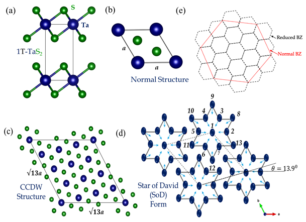
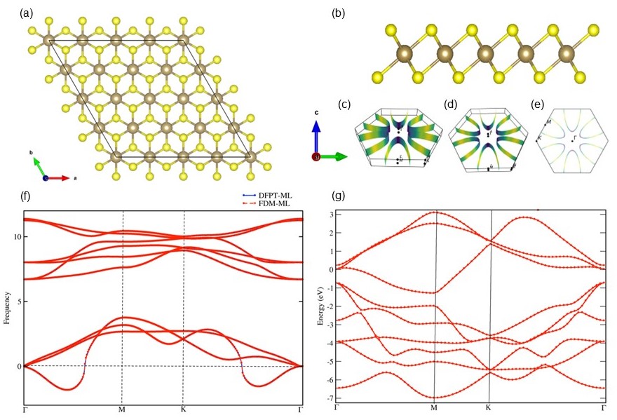
Commensurate Charge Density Wave States: The CDW in 1T-Ta can exist in various commensurate phases, characterized by different periodicity. These phases include 4a, 4a+b, 5a, 6a, and more complex superlattice structures. Each commensurate CDW phase exhibits distinct electronic properties and ordering patterns. In this regard, x-ray scattering experiments revealed the formation of a 5a CDW phase with a periodicity of five times the lattice constant, leading to the formation of an unusual quasi-periodic superlattice 37. The CDW-induced structural reconstruction helps to observe the electronic modulations. Our obtained band structures for bulk and monolayer CCDW 1T-Ta phases are shown in Figure 2 and Figure 3, respectively. The resulting minimizing forces and stress of structure relaxation are reconstructed as SOD phase. It shows the unit cell of the periodic lattice distortions (PLD) and SOD clusters in the Ta plane (shown in Figure 4). Here, the commensurate phase of the CDW phase can only be computationally accessible for periodic DFT simulations, thus we focus of the commensurate-CDW (CCDW) phase. Moreover, it is noticed that the superlattice unit cell contains maximum three types of non-equivalent Ta atoms. Here, a=+3 and b=4- and c= are the three lattice vectors in the CCDW phase that form the superlattice with these in-plane basis vectors. Here, , and parameters follow the lattice vectors as per the hexagonal 1T-Cd type structure.
Fermi surface nesting (FSN): The photoemission matrix element effects can influence the observed Fermi surface nesting (FSN) in 1T-Ta with commensurate CDW phases 37. Here, FSN refers to the alignment of Fermi surface portions that can facilitate the formation of CDWs through the scattering of electrons between these portions. The photoemission matrix element effects modify the photoemission spectra and, consequently, affect the observed the FSN (refer to Figure 3). In 1T-Ta, the CDWs introduce an intricate reconstruction of the electronic structure, leading to the opening of partial band gaps and modifications in the Fermi surface topology (i.e. the Fermi surface states, FSS). The photoemission matrix elements, which depend on the electronic and lattice structure, can enhance or suppress specific spectral features in the photoemission spectra 38, 39, relevant near the CDW-induced band gaps contributing the observed nesting behavior.
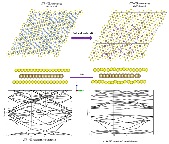
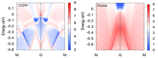
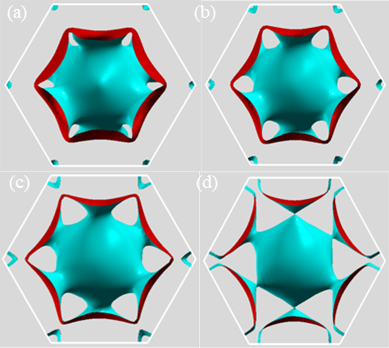
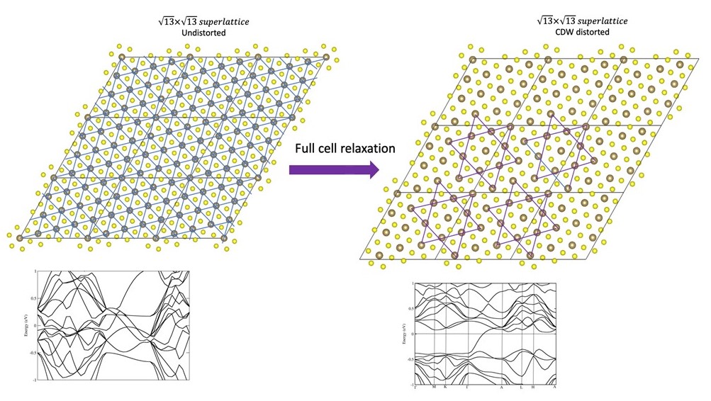
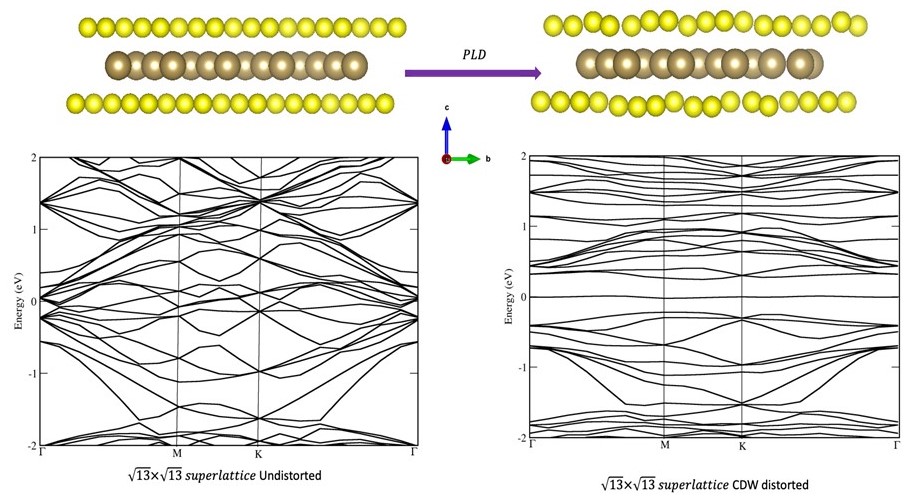
In the present calculations, rev-vdW-DF2 vdW corrections has been included in the structural calculations due to the size and lower symmetry in the distorted superlattice unit cell CCDW phase for better computational accuracy. We optimize the atomic positions within the superlattice providing slight in-plane displacements randomly within 1-3 to Ta atoms to break the symmetry. The atoms relaxed to a CCDW phase spontaneously. Thus, the PLD transforms the normal 1T phase into the CCDW phase, leading to SOD cluster formation. For clarity and better understanding, surface states of Wannier bands are plotted in both cases (shown in Figure 5) and compared with Wannier90 band structure to realize the instability in the CCDW phase. It is obvious to notice the effect of Fermi energy on FSN of the CCDW phases which is shown for various Fermi energies (refer to Figure 6), where the Fermi surface elliptical pockets are showing change in shape. We have plotted the band structure and partial DOS for bulk (shown in Figure 7) and monolayer (shown in Figure 8) phase.
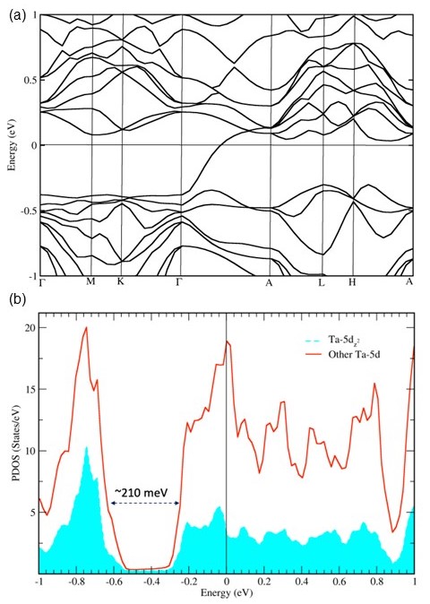
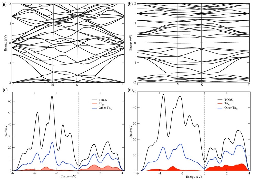
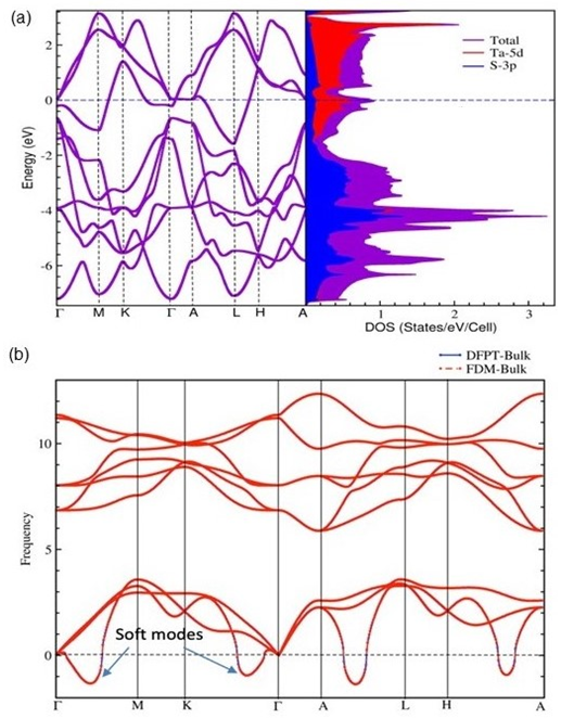
Bulk CCDW states start forming BY unit cells that are commensurate with the original 1T phase of Ta bulk structure. The initial cell volume and lattice positions follow high-symmetry structure based undistorted unit cell (P-3m1 space group 164), which is considered as the normal phase at room temperature and no signature of distortions. Here in this undistorted unit cell, we add slight in-plane displacements randomly to all the in-plane coordinates of Ta atoms ranging from 1 to 3. This addition imposes periodic lattice distortions on the structure creating suitable platform to gain CCDW phase superlattice unit cell. This distorted unit cell undergoes full cell relaxation in the framework of the DFT simulation. Figure 7 shows the electronic band structure and partial DOS (PDOS) plots for bulk CCDW phase, where as the monolayer counterpart are shown in Figure 8.
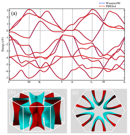
Periodic lattice distortions in CCDW phase- The normal phase 1T-Ta system takes high symmetry state P-3m1 (Space group 164). We performed full wanniersization of Ta d-orbitals using WANNIER90 and check its convergence with DFT band structure for high symmetry phase. Fermi surface has been plotted from the WANNIER90 results and visualized using XCrysDen software 40 (shown in Figure S1). In the superlattice unit cell, total 13 Tantalum (Ta) atoms and 26 Sulfur (S) atoms present to form the structure. To obtain the commensurate CDW phase from this superlattice undistorted unit cell, we induce a periodic lattice distortions into all the Ta atoms centering one Ta atoms. A random displacement (within 1-3) to all 12 Ta atoms has been performed in-plane coordinates following a full cell relaxation. After relaxation, we get the distorted CCDW phase of 1T-Ta superlattice unit cell (shown in Figure S2). We checked both bulk ((shown in Figure S3)) and monolayer ((shown in Figure S4)) cases of CCDW phase and notice the up-gradation in electronic band structures and formation of the Star of David (SOD) clusters. The underneath mechanism of FSN in 1T-Ta with commensurate CDW phases is intimately linked to the PLD that accompany the CDW formation. These distortions are crucial for the emergence of nesting conditions, enabling the scattering of electrons between Fermi surface portions and facilitating the formation of CDWs. The specific details of the nesting mechanism, including the nesting vectors and the resulting CDW wave vectors, depend on the characteristics of the lattice distortions and the resulting band folding in the material. Understanding and controlling these mechanisms are crucial for exploring the rich physics and potential applications of CDW materials like 1T-Ta.
Discussions- One possible explanation for the primary goal of this chirality may be given by the superlattice reconstruction. One symmetry k-point () is present in the first Brillouin zone (BZ) represented by an effective wave vector in case of normal undistorted unit cell. Similarly, the CCDW distorted phase takes additional two cases of symmetry k-points, showing perfect reduction in the BZ wave vectors. This proper reduction in BZ wave vectors are framed as dashed smaller hexagons of black coloured for reduced BZ of distorted CCDW phase and solid big hexagon of red coloured as BZ of undistorted normal phase, having 13. rotation between normal and CCDW phase BZ (shown in the inset of Figure 1). Moreover, elliptical Fermi surface pockets are marked in normal phase to understand the nesting and rotational directions of the reconstructed CCDW phase. Our first principle simulation result is consistent with photoemission matrix elements data, where one Ta-5d band crosses the Fermi level (), forming 06 oval-type packets surrounding the BZ boundaries. Meanwhile, the CDW potential retains the BZ in the CCDW phase and the Fermi surface reconstructs into multiple reduced spots with (×)R13. periodicity. Thus, the three types of BZ points may be responsible for the possible polarization directions 41, 42, 43.
We can notice that Ta atoms are distorted towards the central Ta atoms of the SOD cluster (Figure 2). We find the a-b and a-c interatomic distances that compressed by 4.7 (4.5 expt. value) and 3.2 (2.9 expt. value), respectively which is in close agreement with experimental report 27. Mostly, the Ta atoms distort in-plane direction, so S atoms displace towards out-plane direction (Figure 1, bottom right panel) due to the Ta interatomic compression. Figure LABEL:figure-3 shows the band structure of CCDW phase that is different from the bulk phase. Here, an in-plane band gap opens at the Fermi level, which is the most noticeable fact. Here, Ta d-bands form strongly localized bands up to -1.0 eV the valence band below Fermi level. It is observed that the uppermost p-bands are localized near to -1.48 eV, which is in agreement with experiment 44, 45. This supports the projected density of states and electronically driven instability via Fermi surface nesting in the bulk CCDW phase.
The reconstructed electronic structure and photoemission matrix element effects in 1T-Ta with CCDW phase have been extensively studied using and theoretical techniques. The CDW-induced structural transitions result in the formation of energy gaps, modified band dispersions, and localized states within the gaps. Different CCDW phases exhibit distinct electronic properties and ordering patterns. The interpretation of photoemission data requires accounting for the photoemission matrix element effects, which can significantly impact the observed spectral features. Furthermore, the electronic structure and CDW phases in 1T-Ta can be manipulated by external perturbations, providing opportunities for potential applications in future electronic devices.
Conclusions- In this study, we investigate the electronic structure of 1T-Ta to gain insights into the correlation origin of both the FSN and CDW phases using ab initio density functional theory (DFT) simulations. Our focus lies on the importance of matrix elements in FSN, next to the free electron case. The results obtained for the 1T-Ta system, which are in agreement with calculations using the Wannier90 package, emphasize the necessity of including matrix elements to accurately capture the true instabilities in 1T-Ta. Furthermore, the observation of soft phonon modes provides supporting evidence for the presence of instability, leading the system to enter a distorted CCDW phase. In such cases, achieving perfect nesting may be challenging, as the energy loss due to the distortion of the electronic density quantitatively outweighs the energy gain from lattice distortions. Additionally, the relationship between electronic and lattice distortions requires further investigation. Nonetheless, it is evident that the correlation interaction is strongly influenced by the matrix elements. These findings highlight the need for considering matrix element calculations in order to make reliable predictions about instabilities stemming from FSN, and they pave the way for further exploration of the rich physics associated with this system.
Acknowledgements The authors acknowledge UGC, Government of India for Dr. D. S. Kothari Postdoctoral Fellowship funding No. F.4-2/2006(BSR)/PH/20-21/0108 (dated September 14, 2021). Parts of the simulations are also performed in Parampravega and RN Cluster facility of SERC, IISc.
Author Contributions
S.K.B. and P.C.R. formulated the problem, S.K.B. conducted all the work and analysis. Both the authros wrote the draft.
Notes
The authors declare no competing financial interest.
Keywords
Reconstructed Electronic Structure; Photoemmision Matrix Element; TMDC Material; Quantum Sensing; Quantum Information Science
References
- Xi et al. 2016 Xi, X.; Berger, H.; Forró, L.; Shan, J.; Mak, K. F. Gate Tuning of Electronic Phase Transitions in Two-Dimensional . Phys. Rev. Lett. 2016, 117, 106801
- Kvashnin et al. 2020 Kvashnin, Y.; VanGennep, D.; Mito, M.; Medvedev, S. A.; Thiyagarajan, R.; Karis, O.; Vasiliev, A. N.; Eriksson, O.; Abdel-Hafiez, M. Coexistence of Superconductivity and Charge Density Waves in Tantalum Disulfide: Experiment and Theory. Phys. Rev. Lett. 2020, 125, 186401
- El Baggari et al. 2020 El Baggari, I.; Sivadas, N.; Stiehl, G. M.; Waelder, J.; Ralph, D. C.; Fennie, C. J.; Kourkoutis, L. F. Direct Visualization of Trimerized States in . Phys. Rev. Lett. 2020, 125, 165302
- Martin et al. 2008 Martin, I.; Blanter, Y. M.; Morpurgo, A. F. Topological Confinement in Bilayer Graphene. Phys. Rev. Lett. 2008, 100, 036804
- Yang et al. 2022 Yang, H. F. et al. Visualization of Chiral Electronic Structure and Anomalous Optical Response in a Material with Chiral Charge Density Waves. Phys. Rev. Lett. 2022, 129, 156401
- Jaouen et al. 2023 Jaouen, T.; Pulkkinen, A.; Rumo, M.; Kremer, G.; Salzmann, B.; Nicholson, C. W.; Mottas, M.-L.; Giannini, E.; Tricot, S.; Schieffer, P.; Hildebrand, B.; Monney, C. Carrier-Density Control of the Quantum-Confined Charge Density Wave. Phys. Rev. Lett. 2023, 130, 226401
- Chi et al. 2018 Chi, Z.; Chen, X.; Yen, F.; Peng, F.; Zhou, Y.; Zhu, J.; Zhang, Y.; Liu, X.; Lin, C.; Chu, S.; Li, Y.; Zhao, J.; Kagayama, T.; Ma, Y.; Yang, Z. Superconductivity in Pristine at Ultrahigh Pressure. Phys. Rev. Lett. 2018, 120, 037002
- Wu et al. 2019 Wu, F.; Lovorn, T.; Tutuc, E.; Martin, I.; MacDonald, A. H. Topological Insulators in Twisted Transition Metal Dichalcogenide Homobilayers. Phys. Rev. Lett. 2019, 122, 086402
- Tiemann et al. 2008 Tiemann, L.; Lok, J. G. S.; Dietsche, W.; von Klitzing, K.; Muraki, K.; Schuh, D.; Wegscheider, W. Exciton condensate at a total filling factor of one in Corbino two-dimensional electron bilayers. Phys. Rev. B 2008, 77, 033306
- Behera et al. 2021 Behera, S. K.; Ahalawat, M.; Jana, S.; Samal, P.; Deb, P. Renormalization group analysis of weakly interacting van der Waals Fermi system. Journal of Physics: Condensed Matter 2021, 33, 335604
- Lee et al. 2011 Lee, Y.; Clement, C.; Hellerstedt, J.; Kinney, J.; Kinnischtzke, L.; Leng, X.; Snyder, S. D.; Goldman, A. M. Phase Diagram of Electrostatically Doped . Phys. Rev. Lett. 2011, 106, 136809
- Keimer et al. 2015 Keimer, B.; Kivelson, S. A.; Norman, M. R.; Uchida, S.; Zaanen, J. From quantum matter to high-temperature superconductivity in copper oxides. Nature 2015, 518, 179–186
- Crépel and Fu 2023 Crépel, V.; Fu, L. Anomalous Hall metal and fractional Chern insulator in twisted transition metal dichalcogenides. Phys. Rev. B 2023, 107, L201109
- Behera and Deb 2018 Behera, S. K.; Deb, P. PAW-mediated ab initio simulations on linear response phonon dynamics of anisotropic black phosphorous monolayer for thermoelectric applications. Phys. Chem. Chem. Phys. 2018, 20, 26688–26695
- Zang et al. 2022 Zang, J.; Wang, J.; Cano, J.; Georges, A.; Millis, A. J. Dynamical Mean-Field Theory of Moiré Bilayer Transition Metal Dichalcogenides: Phase Diagram, Resistivity, and Quantum Criticality. Phys. Rev. X 2022, 12, 021064
- Ying et al. 2018 Ying, J.; Paudyal, H.; Heil, C.; Chen, X.-J.; Struzhkin, V. V.; Margine, E. R. Unusual Pressure-Induced Periodic Lattice Distortion in . Phys. Rev. Lett. 2018, 121, 027003
- Shen et al. 2007 Shen, D. W.; Xie, B. P.; Zhao, J. F.; Yang, L. X.; Fang, L.; Shi, J.; He, R. H.; Lu, D. H.; Wen, H. H.; Feng, D. L. Novel Mechanism of a Charge Density Wave in a Transition Metal Dichalcogenide. Phys. Rev. Lett. 2007, 99, 216404
- Chen et al. 2015 Chen, P.; Chan, Y.-H.; Fang, X.-Y.; Zhang, Y.; Chou, M. Y.; Mo, S.-K.; Hussain, Z.; Fedorov, A.-V.; Chiang, T.-C. Charge density wave transition in single-layer titanium diselenide. Nature Communications 2015, 6, 8943
- Soumyanarayanan et al. 2013 Soumyanarayanan, A.; Yee, M. M.; He, Y.; van Wezel, J.; Rahn, D. J.; Rossnagel, K.; Hudson, E. W.; Norman, M. R.; Hoffman, J. E. Quantum phase transition from triangular to stripe charge order in NbSe<sub>2</sub>. Proceedings of the National Academy of Sciences 2013, 110, 1623–1627
- Blöchl 1994 Blöchl, P. E. Projector augmented-wave method. Phys. Rev. B 1994, 50, 17953–17979
- Kresse and Joubert 1999 Kresse, G.; Joubert, D. From ultrasoft pseudopotentials to the projector augmented-wave method. Phys. Rev. B 1999, 59, 1758–1775
- Kresse and Hafner 1993 Kresse, G.; Hafner, J. Ab initio molecular dynamics for liquid metals. Phys. Rev. B 1993, 47, 558–561
- Kresse and Hafner 1994 Kresse, G.; Hafner, J. Ab initio molecular-dynamics simulation of the liquid-metal–amorphous-semiconductor transition in germanium. Phys. Rev. B 1994, 49, 14251–14269
- Kresse and Furthmüller 1996 Kresse, G.; Furthmüller, J. Efficient iterative schemes for ab initio total-energy calculations using a plane-wave basis set. Phys. Rev. B 1996, 54, 11169–11186
- Kresse and Furthmüller 1996 Kresse, G.; Furthmüller, J. Efficiency of ab-initio total energy calculations for metals and semiconductors using a plane-wave basis set. Computational Materials Science 1996, 6, 15–50
- Csonka et al. 2009 Csonka, G. I.; Perdew, J. P.; Ruzsinszky, A.; Philipsen, P. H. T.; Lebègue, S.; Paier, J.; Vydrov, O. A.; Ángyán, J. G. Assessing the performance of recent density functionals for bulk solids. Phys. Rev. B 2009, 79, 155107
- Spijkerman et al. 1997 Spijkerman, A.; de Boer, J. L.; Meetsma, A.; Wiegers, G. A.; van Smaalen, S. X-ray crystal-structure refinement of the nearly commensurate phase of in -dimensional superspace. Phys. Rev. B 1997, 56, 13757–13767
- Grimme et al. 2010 Grimme, S.; Antony, J.; Ehrlich, S.; Krieg, H. A consistent and accurate ab initio parametrization of density functional dispersion correction (DFT-D) for the 94 elements H-Pu. The Journal of Chemical Physics 2010, 132, 154104
- Grimme et al. 2011 Grimme, S.; Ehrlich, S.; Goerigk, L. Effect of the damping function in dispersion corrected density functional theory. Journal of Computational Chemistry 2011, 32, 1456–1465
- Togo and Tanaka 2015 Togo, A.; Tanaka, I. First principles phonon calculations in materials science. Scr. Mater. 2015, 108, 1–5
- Mostofi et al. 2008 Mostofi, A. A.; Yates, J. R.; Lee, Y.-S.; Souza, I.; Vanderbilt, D.; Marzari, N. wannier90: A tool for obtaining maximally-localised Wannier functions. Computer Physics Communications 2008, 178, 685–699
- Grasset et al. 2019 Grasset, R.; Gallais, Y.; Sacuto, A.; Cazayous, M.; Mañas Valero, S.; Coronado, E.; Méasson, M.-A. Pressure-Induced Collapse of the Charge Density Wave and Higgs Mode Visibility in . Phys. Rev. Lett. 2019, 122, 127001
- SUG 1981 Comparison of the soft modes in tantalum dichalcogenides. Physica B+C 1981, 105, 405–409
- Rossnagel and Smith 2006 Rossnagel, K.; Smith, N. V. Spin-orbit coupling in the band structure of reconstructed . Phys. Rev. B 2006, 73, 073106
- Rossnagel 2011 Rossnagel, K. On the origin of charge-density waves in select layered transition-metal dichalcogenides. Journal of Physics: Condensed Matter 2011, 23, 213001
- Pasquier and Yazyev 2022 Pasquier, D.; Yazyev, O. V. Ab initio theory of magnetism in two-dimensional . Phys. Rev. B 2022, 105, L081106
- Yue et al. 2023 Yue, L.; Pokharel, A. R.; Demsar, J.; Zhang, S.; Li, Y.; Dong, T.; Wang, N. Highly anisotropic transient optical response of charge density wave order in . Phys. Rev. B 2023, 107, 165115
- Brouet et al. 2008 Brouet, V.; Yang, W. L.; Zhou, X. J.; Hussain, Z.; Moore, R. G.; He, R.; Lu, D. H.; Shen, Z. X.; Laverock, J.; Dugdale, S. B.; Ru, N.; Fisher, I. R. Angle-resolved photoemission study of the evolution of band structure and charge density wave properties in (, La, Ce, Sm, Gd, Tb, and Dy). Phys. Rev. B 2008, 77, 235104
- Muechler et al. 2022 Muechler, L.; Badrtdinov, D. I.; Hampel, A.; Cano, J.; Rösner, M.; Dreyer, C. E. Quantum embedding methods for correlated excited states of point defects: Case studies and challenges. Phys. Rev. B 2022, 105, 235104
- Kokalj 1999 Kokalj, A. XCrySDen—a new program for displaying crystalline structures and electron densities. Journal of Molecular Graphics and Modelling 1999, 17, 176–179
- Wang et al. 2020 Wang, Y. D.; Yao, W. L.; Xin, Z. M.; Han, T. T.; Wang, Z. G.; Chen, L.; Cai, C.; Li, Y.; Zhang, Y. Band insulator to Mott insulator transition in 1T-TaS2. Nature Communications 2020, 11, 4215
- Lacinska et al. 2022 Lacinska, E. M.; Furman, M.; Binder, J.; Lutsyk, I.; Kowalczyk, P. J.; Stepniewski, R.; Wysmolek, A. Raman Optical Activity of 1T-TaS2. Nano Letters 2022, 22, 2835–2842
- Yu et al. 2017 Yu, X.-L.; Liu, D.-Y.; Quan, Y.-M.; Wu, J.; Lin, H.-Q.; Chang, K.; Zou, L.-J. Electronic correlation effects and orbital density wave in the layered compound . Phys. Rev. B 2017, 96, 125138
- Manzke et al. 1989 Manzke, R.; Buslaps, T.; Pfalzgraf, B.; Skibowski, M.; Anderson, O. On the Phase Transitions in 1T-TaS2. Europhysics Letters 1989, 8, 195
- Sato et al. 2014 Sato, H.; Arita, M.; Utsumi, Y.; Mukaegawa, Y.; Sasaki, M.; Ohnishi, A.; Kitaura, M.; Namatame, H.; Taniguchi, M. Conduction-band electronic structure of 1-TaS2 revealed by angle-resolved inverse-photoemission spectroscopy. Phys. Rev. B 2014, 89, 155137
Supplementary Materials