Quantum size effects on Andreev transport in Nb/Au/Nb Josephson junctions:
A combined ab-initio and experimental study
Abstract
We have measured the critical current density, superconducting coherence length, and superconducting transition temperature on single-domain, epitaxially-grown Nb(110)/Au(111)/Nb(110) trilayers, all showing non-monotonic behavior as a function of the thickness of the Au layer. To reveal the underlying physical mechanism, we apply the first-principles-based microscopic theory of inhomogeneous relativistic superconductivity which predicts quantitatively the superconducting properties. As a result of the confinement in the growth direction, quantum-well states appear in the Au layer which yields a complex structure of Andreev states in the superconducting state. It is shown how the quantum-well states modify the quasiparticle spectrum and the Josephson supercurrent. Our study reveals the coexistence of the two superconducting phases in the Au layer, the usual intraband -wave phase and an additional non-uniform phase stemming from interband pairing (without magnetic field). These results indicate the rich interplay between quantum-size and proximity effects, suggesting the possibility of modifying superconducting transport properties by exploiting thickness-dependent quantum size effect.
The characteristic feature of superconductors (SCs) is the macroscopic occupation of bound pairs of electrons, known as Cooper pairs, in the same quantum-coherent ground state described by a complex superconducting order parameter (SOP). In homogeneous -wave SCs this is accompanied by a fully gapped quasiparticle spectrum. However, if the SOP varies in space, lower energy, subgap excitations may be formed. These, so called Andreev Bound States (ABS), are the consequence of Andreev scattering in which an incoming electron-like state can convert into an outgoing hole-like one[1]. The classical example of such systems is the superconductor - normal metal - superconductor (SNS) junctions which is characterized by a non-zero phase difference between the SOP belonging to the two superconductors. It was predicted that the ABS depends strongly on the phase difference between the SCs [2, 3] and it is responsible for the flow of the Josephson supercurrent[4]. Josephson junctions are among the most active areas of research in superconducting spintronics[5, 6, 7, 8, 9, 10]. They are mostly driven by the rapid progress in growth and characterization techniques[11, 12, 13, 14]. However, little attention is paid to the actual effects of the realistic band structure, which is likely to be very significant for short junctions where there is a quantum confinement of electrons in the growth direction. If the characteristic size of the metal is of the order of the bulk Fermi wavelength, the in-gap band structure (and consequently the Fermi surface as well) splits into a series of subbands, known as quantum-well states (QWSs), leading to multiband superconductivity.
In this paper we show that, in epitaxial Nb(110)/Au(111)/Nb(110) trilayers, the critical current density, the superconducting coherence length and the superconducting transition temperature are all oscillating as a function of the Au-layer thickness. Although 0- phase transitions (meaning that the phase of the SOP is inverted between two superconducting leads) are usually connected to a similar oscillatory behavior, we show that these oscillations are intrinsic to the proximitized QWS in the Au(111) layer. We develop a detailed microscopic theory based on the Kohn-Sham-Dirac-Bogoliubov-de Gennes (KS-DBdG) equations, which allow us to quantitatively predict the superconducting properties including the quasiparticle spectrum and the Josephson supercurrent by involving the details of the electronic structure together with spin-orbit coupling (SOC). This theory reveals that, although the Au layer is disorder-free in the ab-initio description, the layer-dependent electronic structure causes extra scattering - similarly to impurities - and transforms the Josephson supercurrent from the ballistic to the tunneling limit. Moreover, it predicts the spontaneous appearance of a non-uniform phase, which can be associated with crossing QWS near the Fermi level, and yet again is the consequence of multiband behavior.
The starting point of our study is a series of experiments performed on Nb(110)/Au(111)/Nb(110) trilayer samples with vaious Au thicknesses () prepared on single crystals of Al2O using molecular-beam-epitaxy. One atomic gold monolayer (1 ML) corresponds to nm. Epitaxial layer-by-layer growth occured without structural change for nm. The details of the sample preparation and structural characterization can be found in the Supplemental Material[15]. For the superconducting transition temperature, shall be defined as the temperature at 50% of the residual resistivity, and is as the onset point of the diamagnetic transition. Typical temperature dependences of normalized resistivity and of normalized magnetic susceptibility can be found in the Supplemental Material[15].
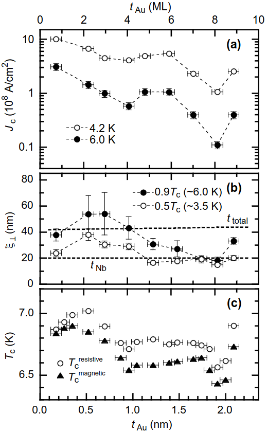
The average electron mean free paths nm and nm were calculated from the residual resistivity as a function of by performing a theoretical fit using a parallel register model. We also estimated the superconducting coherence lengths and from the measurements of the upper critical fields and using the expressions: and where is the flux quantum and the directions, and , are referred to with respect to the surface. The superconducting coherence length of the Nb layer extrapolated to zero Kelvin was found to be nm. These results imply that the charge transport through the Au spacer layer is in the clean limit ( ) and the superconductivity of the Nb layers is in the dirty limit ( ). We also point out that the sample total thickness, nm (excluding the substrate) shown in Fig. 1(b), is comparable to the field-penetration depth of nm in bulk Nb. The superconducting critical current density in zero magnetic field was estimated from the hysteresis curve based on the Bean model[15] and the results for are shown in Fig. 1(a). For samples with nm (2 ML) disorder was more pronounced, however in case of samples with 2 ML over a range of temperatures 3.5 K, the temperature dependence of is well-described by the expression , with . This is in good agreement with the exponent obtained for critical current at 0 Oe in an 120 nm thick Nb film[16]. Ginzburg-Landau theory predicts near [17]. The values of seen in Fig. 1(a) are extremely high, relative to the SC/FM/SC (FM: ferromagnet) systems studied so far[5].
The proximity effect in these Nb(110)/Au(111)/Nb(110) trilayers also displays a number of features. As shown in Fig. 1, neither , , nor are smooth, monotonic functions of the thickness . In particular, there are sharp features at nm (4 ML) and 1.88 nm (8 ML). We wish to emphasize that, at these thicknesses, there are no changes in crystal structure and the observed modulation in and is therefore intrinsic to Nb(110)/Au(111)/Nb(110) trilayers. Such systematic, non-monotonic variations in and as functions of the nonmagnetic-layer thickness have not been reported before, and we infer that epitaxially grown multilayer systems of equivalently high quality are necessary for it to be observed.
On one hand, theoretically, transport phenomena is usually studied in terms of a quasiclassical approach which typically involves either Eilenberger equations[18] for ballistic systems or Usadel equations[19] to describe the limit of strong disorder. On the other hand, the quasiclassical picture is valid only if the Fermi wavelength is much smaller than any other length scale of the problem. Because certain information has been integrated over in the equations, they represent a less sophisticated theory compared to the BdG equations. Moreover, it has been recently shown that the first-principles treatment of the electronic structure is necessary even for understanding the supercurrent decay in magnetic Josephson junctions [20]. Therefore, to properly account for the realistic electronic structure involving the multiorbital nature together with spin-orbit coupling treated on the same footing, we solve the following fully relativistic KS-DBdG Hamiltonian written in Rydberg units
| (1) |
where , with , , , denotes the Pauli-matrices, and being the identity matrix of order . and are the effective potential and the exchange field, respectively. is the effective pairing potential matrix due to the four component Dirac spinors. The KS-DBdG equations should be solved self-consistently, which, for layered systems can be achieved most efficiently by the Screened Korringa-Kohn-Rostoker Green’s function (SKKR-GF) method[21, 22] by assuming that the superconducting host has isotropic -wave spin-singlet pairing. The description of the formalism and the computational details can be found in the Supplemental Material[15].
We carried out normal state band structure calculations using the layered SKKR-GF method for various thicknesses of the Au layer (0-12 ML) between two semi-infinite Nb. As shown in Fig. 2 the electronic structure contains several interesting features. Based on the DOS shown in Fig. 2(a) we argue that the electronic structure changes the most up to 4 ML Au thickness due to charge transfer at the interface. Figure 2(b-c, e-f) show the Fermi surfaces and band structure of the middle Au monolayer for 3 and 9 ML Au thicknesses along a high symmetry line in the Brillouin zone (BZ). The figure nicely demonstrates that QWSs are formed with increasing thickness and the appearance of the Au’s relative band gap in Fig. 2(c). These QWSs are standing electron waves quantized in the direction perpendicular to the surface, while parallel to the surface the bands typically show a free electron-like dispersion. When a new subband related to this QWS behavior intersects the Fermi level, the electronic properties can change quite dramatically. We mention that the oscillatory behavior of superconducting properties due to QWS has been reported for superconducting lead thin films[11] (including the critical temperature[23] and critical field[12, 24]). Another important observation is the appearance of a Dirac-like state in the middle of the Au layer at the edge of the BZ which has an intersection point for 9 ML on the Fermi surface. In principle, the electronic structure suggests that interband scattering mechanisms can be at play, including specular interband Andreev reflection[25] and interband pairing leading to Fulde-Ferrel-Larkin-Ovchinnikov (FFLO)[26, 27] type non-uniform phase[28].
One can also observe that some states in the Au layer are smeared out: this happens in the -space regions where the DOS is high in the Nb, since the appropriate electrons can scatter more easily into the other side of the interface. Another interesting problem is the effect of SOC.One may expect Rashba-type SOC and corresponding splitting of the states due to the interfaces of Nb/Au/Nb. However, no SOC induced band splitting can be observed in the band structure around the Fermi level. This would clearly not be the case for a pure surface, where the symmetry breaking would be more apparent. We argue that the existence of a surface/interface itself in an inversion symmetric junction is not a sufficient condition to lift Kramers’ degeneracy. In fact, it was reported that free-standing Au(111) slabs do not show band splitting in the repeated-slab model, since there is no asymmetry between the two surfaces[29, 30].
By solving the KS-DBdG equations we obtained the quasiparticle spectrum for various Au thicknesses (0-12 ML) which allows the quantitative prediction of current-phase relationship (CPR) corresponding to the Josephson supercurrent[31], written in Ry units as
| (2) |
The critical current is associated with the maximum of the Josephson supercurrent that can exist through the junction. In a real experimental situation, one passes a current across the Josephson junction which reacts by changing the phase difference between the superconducting leads. The values obtained for the critical current are shown in Fig. 2(d). One can see that there is a good qualitative agreement between the results obtained by the first-principles-based calculations and those by experimental study. In what follows, we further analyze the features of the superconducting state to explain the obtained behavior.
In general, CPR can be expanded in Fourier harmonics as . Although in many cases, the CPR can be reasonably described by the first harmonics, the sinusoidal shape is not always preserved. At a microscopic level, the supercurrent through a short junction is determined by bound states forming in the confinement due to Andreev reflection. In the short junction limit assuming scattering events in the conduction channel with a transmission , the Andreev levels are given by[32] which yields the well-known sinusoidal shape[3]. In fact, the sinusoidal shape was obtained in the tunneling limit (meaning the transmission ) first by Ambegaokar[33]: with where is the normal state resistivity. However, in the ballistic limit () at 0 K, the Josephson current[34] is which has twice as large amplitude compared to the tunneling limit, and it shows an anomalous discontinuity at .
The quasiparticle DOS and the supercurrents as a function of are shown in Fig. 3(a-e). In Fig. 3(a) we show a hypothetical scenario where two semi-infinite Nb with a phase difference are touched together. The quasiparticle spectrum shows a well-defined -dependent ABS recovering the result: and yields the supercurrent (Fig. 3(d)) showing discontinuity at at 0 K which corresponds to the analytical result of Ambegaokar[33]. In Fig. 3(b) the quasiparticle DOS is shown for an Nb/Au/Nb junction with ML. Striking contrast can be observed compared to the case where two semi-infinite Nb were touched. Several ABS can be observed changing with and in fact they form an almost continuous spectrum within the superconducting gap region. Although the Au layers can be considered in the clean limit (absence of impurities), the different band structures of Nb and Au can cause a similar effect as the impurities with varying strength of transmission for different wavenumbers . We stress that this picture is also supported by the findings in Ref. 20 where it was shown that the electronic structure has similar effects on the FFLO state as expected for impurities. Corresponding to this picture (tunneling limit), in Fig. 3(e) the supercurrent ( ML) shows the usual sinusoidal shape. Therefore, we argue that the anomalous changes in the superconducting properties around ML in Fig. 1 are related to the rapid change of the electronic structure from the ballistic to the tunneling limit (see also the Supplemental Material[15]) which causes a drop in the critical current, superconducting transition temperature and coherence length. For ML interface disorder occurred in the region of 2 ML thickness between the lower-Nb and the Au layer, therefore, the increases slightly up to 2 ML as the disorder continuously eliminated with growing thickness. However, as we have seen in Fig. 2 the DOS at the Fermi level significantly decreases up to 4 ML (corresponding to the change from the ballistic to the tunneling limit) which lowers the critical temperature since . Similarly, the changes in the measured perpendicular coherence length also fit this theory. In the ballistic limit (up to 4 ML) one experiences larger coherence length compared to the tunneling limit (for ML interface disorder tends to drive the system into the tunneling limit).
Interestingly, in Fig. 1 the experimental also shows anomalous behavior at ML. Corresponding to this, we show the quasiparticle DOS for ML in Fig. 3(c) where an additional feature can be observed: even at a well-defined striking ABS is present which also changes in energy with the variation of giving a kick to the critical current (shown in Fig. 2(d)). We argue that this ABS is related to the QWS obtained at the edge of the BZ (see Fig. 2(f)), where several QWSs get close to each other and crossings are observed in the vicinity of the Fermi level. To better understand the nature of this state the normalized energy-resolved singlet order parameter (details in the Supplemental Material[15]) is shown Fig. 3(f): one can clearly observe the non-uniform structure (change in sign within the interface region) with the maximum value obtained in the middle of the Au layer. This is a clear signature of the spontaneous appearance of Cooper pairs with nonzero center-of-mass momentum in the Au layer which was also suggested in Ref. 28. The interesting feature of this state is that it is formed without any magnetic field in the system. Therefore, the discontinuous behavior obtained around ML is related to the appearance of a co-existing non-uniform superconducting phase in the Au layer causing larger critical current and transition temperature.
In summary we have studied the effect of the electronic structure on the proximity effect in Nb(110)/Au(111)/Nb(110) trilayers as a function of the Au layer thickness. We have demonstrated similar behavior of the superconducting properties between the experimental results and the ab-initio based BdG theory which emphasizes the crucial role of the electronic structure in understanding the physics of superconducting heterostructures.
Acknowledgement The authors are pleased to acknowledge helpful conversations with James Annett, Balázs Győrffy, József Cserti and Ilya Vekhter. This work was supported by the Okinawa Institute of Science and Technology Graduate University (Japan), and the Engineering and Physical Sciences Research Council Grant No. EP/G049483/1 (United Kingdom). G.Cs. acknowledges support from Austrian Science Fond (FWF) project No. 33491-N “ReCALL”. K.N. and B.U. acknowledge financial support by the National Research, Development, and Innovation Office (NRDI Office) of Hungary under Project Nos. K131938 and K142652.
References
- Andreev [1964] A. Andreev, Sov. Phys. JETP 19, 1228 (1964).
- Furusaki and Tsukada [1991] A. Furusaki and M. Tsukada, Phys. Rev. B 43, 10164 (1991).
- Sauls [2018] J. A. Sauls, Philosophical Transactions of the Royal Society A: Mathematical, Physical and Engineering Sciences 376, 20180140 (2018).
- Josephson [1962] B. Josephson, Physics Letters 1, 251–253 (1962).
- Buzdin [2005] A. I. Buzdin, Rev. Mod. Phys. 77, 935 (2005).
- Linder and Robinson [2015] J. Linder and J. W. A. Robinson, Nature Physics 11, 307 (2015).
- Eschrig [2015] M. Eschrig, Reports on Progress in Physics 78, 104501 (2015).
- Amundsen et al. [2022] M. Amundsen, J. Linder, J. W. A. Robinson, I. Žutić, and N. Banerjee, Colloquium: Spin-orbit effects in superconducting hybrid structures (2022), arXiv:2210.03549 [cond-mat.supr-con] .
- Nadeem et al. [2023] M. Nadeem, M. S. Fuhrer, and X. Wang, Nature Reviews Physics 5, 558 (2023).
- Mercaldo et al. [2023] M. T. Mercaldo, C. Ortix, and M. Cuoco, Advanced Quantum Technologies 6, 2300081 (2023).
- Guo et al. [2004] Y. Guo, Y.-F. Zhang, X.-Y. Bao, T.-Z. Han, Z. Tang, L.-X. Zhang, W.-G. Zhu, E. G. Wang, Q. Niu, Z. Q. Qiu, J.-F. Jia, Z.-X. Zhao, and Q.-K. Xue, Science 306, 1915–1917 (2004).
- Bao et al. [2005] X.-Y. Bao, Y.-F. Zhang, Y. Wang, J.-F. Jia, Q.-K. Xue, X. C. Xie, and Z.-X. Zhao, Phys. Rev. Lett. 95, 247005 (2005).
- Yamazaki et al. [2006] H. Yamazaki, N. Shannon, and H. Takagi, Phys. Rev. B 73, 094507 (2006).
- Yamazaki et al. [2010] H. Yamazaki, N. Shannon, and H. Takagi, Phys. Rev. B 81, 094503 (2010).
- [15] See Supplemental Material at [URL will be inserted by publisher] for details of the sample preparation and its analysis, the first-principles based treatment of superconducting heterostructures and computational details, the detailed normal state band structures and quasiparticle spectrum. The Supplemental Material also contains Refs. 35, 36, 37, 38, 39, 40, 41, 42, 43, 44, 45.
- Pan et al. [1998] A. Pan, M. Ziese, R. Höhne, P. Esquinazi, S. Knappe, and H. Koch, Physica C: Superconductivity 301, 72–84 (1998).
- Rusanov et al. [2004] A. Y. Rusanov, M. B. S. Hesselberth, and J. Aarts, Phys. Rev. B 70, 024510 (2004).
- Eilenberger [1968] G. Eilenberger, Zeitschrift für Physik A Hadrons and nuclei 214, 195–213 (1968).
- Usadel [1970] K. D. Usadel, Phys. Rev. Lett. 25, 507 (1970).
- Ness et al. [2022] H. Ness, I. A. Sadovskyy, A. E. Antipov, M. van Schilfgaarde, and R. M. Lutchyn, npj Computational Materials 8, 23 (2022).
- Csire et al. [2015] G. Csire, B. Újfalussy, J. Cserti, and B. Győrffy, Phys. Rev. B 91, 165142 (2015).
- Csire et al. [2018] G. Csire, A. Deák, B. Nyári, H. Ebert, J. F. Annett, and B. Újfalussy, Phys. Rev. B 97, 024514 (2018).
- Shanenko et al. [2007] A. A. Shanenko, M. D. Croitoru, and F. M. Peeters, Phys. Rev. B 75, 014519 (2007).
- Wójcik and Zegrodnik [2014] P. Wójcik and M. Zegrodnik, Journal of Physics: Condensed Matter 26, 455302 (2014).
- Beenakker [2006] C. W. J. Beenakker, Phys. Rev. Lett. 97, 067007 (2006).
- Fulde and Ferrell [1964] P. Fulde and R. A. Ferrell, Physical Review 135, A550 (1964).
- Larkin and Ovchinnikov [1964] A. I. Larkin and Y. N. Ovchinnikov, Zh. Eksp. Teor. Fiz. 47, 1136 (1964).
- Wójcik et al. [2019] P. Wójcik, M. P. Nowak, and M. Zegrodnik, Phys. Rev. B 100, 045409 (2019).
- Yakovkin [2018] I. N. Yakovkin, Advances in Condensed Matter Physics 2018, 1–5 (2018).
- Yakovkin [2020] I. Yakovkin, Surface Science 691, 121501 (2020).
- Beenakker [1992] C. W. J. Beenakker, Three “universal” mesoscopic josephson effects, in Springer Series in Solid-State Sciences (Springer Berlin Heidelberg, 1992) p. 78–82.
- Beenakker [1991] C. W. J. Beenakker, Physical Review Letters 67, 3836 (1991).
- Ambegaokar and Baratoff [1963] V. Ambegaokar and A. Baratoff, Phys. Rev. Lett. 10, 486 (1963).
- Kulik and Omelyanchouk [1978] I. O. Kulik and A. N. Omelyanchouk, Le Journal de Physique Colloques 39, C6 (1978).
- Sürgers and Löhneysen [1992] C. Sürgers and H. Löhneysen, Applied Physics A Solids and Surfaces 54, 350–354 (1992).
- Carneiro [1998] G. Carneiro, Phys. Rev. B 57, 6077 (1998).
- Stejic et al. [1994] G. Stejic, A. Gurevich, E. Kadyrov, D. Christen, R. Joynt, and D. C. Larbalestier, Phys. Rev. B 49, 1274 (1994).
- Mawatari and Yamafuji [1994] Y. Mawatari and K. Yamafuji, Physica C: Superconductivity 228, 336–350 (1994).
- Oliveira et al. [1988] L. N. Oliveira, E. K. U. Gross, and W. Kohn, Phys. Rev. Lett. 60, 2430 (1988).
- Sipr and Györffy [1996] O. Sipr and B. L. Györffy, Journal of Physics: Condensed Matter 8, 169–191 (1996).
- Csire et al. [2016a] G. Csire, J. Cserti, I. Tüttő, and B. Újfalussy, Phys. Rev. B 94, 104511 (2016a).
- Csire et al. [2016b] G. Csire, J. Cserti, and B. Újfalussy, Journal of Physics: Condensed Matter 28, 495701 (2016b).
- Suvasini et al. [1993] M. B. Suvasini, W. M. Temmerman, and B. L. Gyorffy, Phys. Rev. B 48, 1202 (1993).
- Szunyogh et al. [1994] L. Szunyogh, B. Újfalussy, P. Weinberger, and J. Kollár, Phys. Rev. B 49, 2721 (1994).
- Zeller et al. [1995] R. Zeller, P. H. Dederichs, B. Újfalussy, L. Szunyogh, and P. Weinberger, Phys. Rev. B 52, 8807 (1995).