[1,2,3,4,5]\fnmA. \surGiachero
1]\orgnameNational Institute of Standards and Technology, \orgaddress\cityBoulder, \postcode80305, \stateColorado, \countryUSA
2]\orgdivDepartment of Physics, \orgnameUniversity of Colorado, \orgaddress\cityBoulder, \postcode80309, \stateColorado, \countryUSA
3]\orgdivDepartment of Physics, \orgnameUniversity of Milano Bicocca, \orgaddress\cityMilan, \postcodeI-20126, \countryItaly
4]\orgnameINFN - Milano Bicocca, \orgaddress\cityMilan, \postcodeI-20126, \countryItaly
5]\orgnameBicocca Quantum Technologies (BiQuTe) Centre, \orgaddress\cityMilan, \postcodeI-20126, \countryItaly
Kinetic inductance traveling wave amplifier designs for practical microwave readout applications
Abstract
A Kinetic Inductance Traveling Wave amplifier (KIT) utilizes the nonlinear kinetic inductance of superconducting films, particularly Niobium Titanium Nitride (NbTiN), for parametric amplification. These amplifiers achieve remarkable performance in terms of gain, bandwidth, compression power, and frequently approach the quantum limit for noise. However, most KIT demonstrations have been isolated from practical device readout systems. Using a KIT as the first amplifier in the readout chain of an unoptimized microwave SQUID multiplexer coupled to a transition-edge sensor microcalorimeter we see an initial improvement in the flux noise [1]. One challenge in KIT integration is the considerable microwave pump power required to drive the non-linearity. To address this, we have initiated efforts to reduce the pump power by using thinner NbTiN films and an inverted microstrip transmission line design. In this article, we present the new transmission line design, fabrication procedure, and initial device characterization – including gain and added noise. These devices exhibit over 10 dB of gain with a 3 dB bandwidth of approximately 5.5–7.25 GHz, a maximum practical gain of 12 dB and typical gain ripple under 4 dB peak-to-peak. We observe an appreciable impedance mismatch in the NbTiN transmission line, which is likely the source of the majority of the gain ripple. Finally we perform an initial noise characterization and demonstrate system-added noise of three quanta or less over nearly the entire 3 dB bandwidth.
keywords:
Quantum noise, parametric amplifier, traveling wave, microwave kinetic inductance detector, detector array read out, qubit read out1 Introduction
Fundamental physics experiments operating at microwave frequencies require ultra-sensitive readout schemes that greatly benefit from a amplification chain with the lowest possible noise, high gain, and large bandwidth. These requirements are essential for the readout of large arrays of detectors without compromising the information conveyed by the signal. Although semiconductor amplifiers, such as high-electron-mobility transistor (HEMT) amplifiers, provide large gain and bandwidths [2], their noise is often times the Standard Quantum Limit (SQL) [3] at microwave frequencies. Josephson parametric amplifiers [4, 5] (JPAs) offer noise performance at or below the SQL. However, their bandwidth is limited to a few hundred megahertz [6] – significantly limiting the number of devices they can practically read out.
An emerging technology for achieving these requirements is that of the broadband TWPA, such as the Josephson TWPA (JTWPA) [7] or the kinetic inductance TWPA (KITWPA) [8], or KIT. These devices reach noise levels near the SQL with high gain over a larger bandwidth (a few GHz). A TWPA amplifier generally consists of a long transmission line designed to exploit a specific nonlinearity in a superconducting circuit. A large pump tone modulates these nonlinear elements, coupling the pump () to a signal () and idler () tone via frequency conversion. In the Four-Wave-Mixing (4WM) case , while for three-wave-mixing (3WM) , i.e. abundant pump photons are exchanged for signal (and idler) photons, resulting exponential signal gain as photons interact with the modulated nonlinearity. In the case of JTWPA, the nonlinearity used is the Josephson inductance[9], while a KIT uses the superconducting nonlinear kinetic inductance [10]. Compared with JTWPAs, KITs are simple to fabricate and require only few lithography and etching steps, without overlapping structures. Additionally, KIT amplifiers based on Niobium Titanium Nitride (NbTiN) thin films provide a high dynamic range (- dBm), gain (20 dB), and operate near the SQL [11]. KITs have been successfully used to read out superconducting qubits [12], Microwave Kinetic Inductance Detectors (MKIDs) [13], Transition Edge Sensor (TESs) [1] and also showed impressive performance operating at 4 K [14].
However, contemporary KITs require a strong pump, typically around -30 dBm at the KIT input [11]. Isolating this power from the device under test is challenging, potentially resulting in excess noise and a degradation of readout channel performance. These devices are based on 20-30 nm NbTiN films with a kinetic inductance, , in the range of 7-10 pH/sq [11, 15]. Reduction of the pump power may be realized by using a thinner superconducting film with a higher kinetic inductance [16]. In this study, we present preliminary results on KITs designed with a target of 35 pH/sq adapted from the previous coplanar waveguide geometry [11] to an inverted microstrip [15].
2 Transmission line design
The kinetic inductance of a superconducting transmission line under dc current bias is , with [11]. Here is an intrinsic material parameter that controls the scale of the kinetic inductance nonlinearity [17]. () is the rf (dc) current, is the NbTiN kinetic inductance at zero dc current, is the line inductance under nonzero dc bias and zero rf current (). describes the 3WM process, while and describes 4WM.
The scaling current is directly proportional to the cross-sectional area of the film (, see Fig. 1), thus decreasing reduces . Moreover, reducing the film thickness results in an increase in , so the required pump power (dc bias) to achieve a given decreases quadratically (linearly) with . Thicknesses of 5 and 10 nm yield kinetic inductance values of approximately 100 pH/sq and 30 pH/sq, respectively – along with scaling currents of about 0.6 mA and 3 mA, respectively[16]. These values should be compared with the previous KIT device: pH/sq and mA [11, 14].
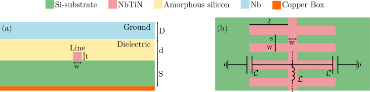
Using an Inverted Microstrip (IMS) geometry, we recently implemented a nm thick NbTiN film to realize of around 35 pH/sq. The -Si thickness is nm. The sky (ground) plane is made of a thick Nb layer ( nm, negligible) deposited on top of the -Si. The microstrip center line and finger widths are m while the spacing between adjacent fingers is m, resulting in a elementary cell length of m (Fig. 1). The line impedance is determined by the inductance (capacitance) per unit length () via . With these dimensions, electromagnetic simulations provided a finger length of m (m) for matching (). The full KIT line is made from a string of 1200 super-cells, each composed of 30 unloaded-cells and 6 loaded-cells. This gives a stop-band around 10.5–11.00 GHz and, since the gain profile is centered near and the pump is applied just above the stop-band, this centers the gain near 6 GHz. The total transmission line length is 8.64 cm.
Beyond shortening the total line length (and thus overall device size) via increasing the kinetic inductance and, as consequence, the inductance per unit length and the stub-to-ground capacitance per unit length, the IMS approach also benefits from significantly higher fabrication yield relative to previous devices implementing a Coplanar Waveguide (CPW) transmission line. Elimination of the potential for a center-ground short (lithographic) failure common in the CPW geometry resulted in a 100% device yield with the new IMS devices. On the other hand, the presence of a non-vacuum dielectric could potentially increase loss and noise, including those sourced from two-level system (TLS) interactions.
3 Device Fabrication
The devices are fabricated on a 76.2 mm, high-resistivity, intrinsically-doped, float-zone Si wafer. Immediately before loading into the vacuum chamber the native oxide is stripped using HF [18]. As for previous designs, the NbTiN is reactively co-sputtered from Ti and Nb targets in an Ar:N2 atmosphere at 500∘C with the rates tuned to maximize the superconducting transition temperature. After the NbTiN growth, the substrate is cooled to room temperature without breaking vacuum and a 50 nm layer of Al is deposited. The wafer is then patterned using an i-line stepper. The Al is etched away using Transene A etchant, which does not attack the NbTiN beneath, only leaving Al in the bondpad regions. The wafer is then re-patterned and the NbTiN is etched using a CHF3 based plasma in an ICP-RIE to define the center strip of the inverted microstrip. This etch does not quickly trench into the Si which could complicate later step coverage, and leaves a surface compatible with high microwave devices [19]. An insulating layer of -Si is deposited at room temperature using ICP-PECVD, and then the ground plane of 100 nm of Nb is sputtered. The ground plane near the bondpads and transition from microstrip to CPW is patterned and etched using a CF4-based RIE, which is selective versus the underlying -Si. Finally, the vias in the -Si are patterned and etched in an SF6 RIE with the etch stopping on the Al covering the bond-pads.
4 Characterization Measurements
On each wafer, we produce both KIT amplifier dies and diagnostic chips. The diagnostic chips are composed of lumped element resonator arrays to directly measure the NbTiN kinetic inductance and -Si permittivity. For the measurement we use an interdigitated capacitor and NbTiN straight segment to form the resonator, while for the permittivity measurement we use a parallel plate capacitor. The KIT dc bias is supplied to the devices using two bias-tees, while the pump signal is attenuated by 10 dB at 4 K and then delivered to the KIT package with a directional coupler. We measure a KIT critical current of 0.38 mA and a scaling current of 2.1 mA, which are compatible with values obtained in an earlier study with the same material [16]. These values are lower compared to those measured for the nm NbTiN CPW version [11] ( mA and mA) as expected.
Gain profile measurements are performed by determining the ratio between the forward transmission with fixed dc bias and the pump on and off. In total, eight devices were tested and all exhibited gain ranging between 10–20 dB (Fig. 2) and centered near 6 GHz. During tune-up of the gain profile ranged from 0.12 to 0.24 mA, and the pump frequency is typically GHz. Higher gain is possible with increased dc bias and pump power at the expense of a larger ripple.
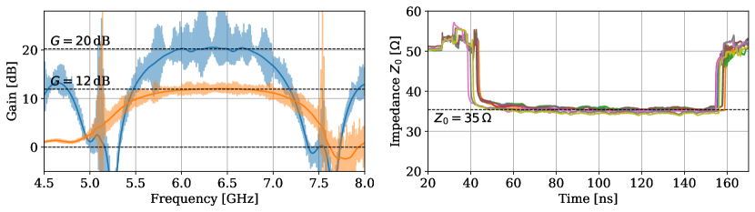
Typical pump powers are comparable to the previous 20 nm NbTiN CPW version (-30 dBm on-chip pump power) [11]. However, the current devices have a much thinner NbTiN film so the required pump power is expected to be lower than the CPW devices and currently under investigation. We also discover an impedance mismatch of the microstrip line using a Time-domain Reflectometry (TDR) measurement which yields a characteristic impedance of (Fig. 2, right). With the diagnostic chips we measured the NbTiN film kinetic inductance to be pH/sq, and the -Si permittivity to be . The latter is substantially discrepant with the expected value from past measurements. Simulations performed with the measured and , yielded a characteristic impedance around .
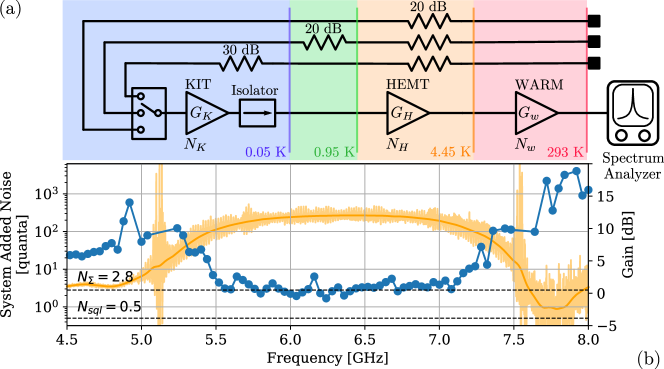
To characterize the system-added noise with the KIT as the first-stage amplifier we use a modified -factor (“hot/cold”) method using three coaxial lines with attenuators at three different temperature stages {20, 20, 30} dB at {4.45, 0.95, 0.05} K. These three noise temperatures are connected to the KIT via a cryogenic micro-electromechanical system (MEMS) switch. A simplified schematic circuit for the noise characterization is shown in Fig. 3(a). Each noise input line is terminated at room temperature so consideration of the entire chain moving from 293 K to the KIT input is necessary to obtain the correct effective temperatures. After a full loss characterization of each component (all at base temperatures) we obtain mean input temperatures of {3.41, 0.55, 0.16} K, or {11.0, 1.8, 0.7} quanta across the KIT bandwidth.
To estimate the KIT-on system-added noise we measure the system output power level using a Spectrum Analyzer (SA) configured in zero-span mode with 1 MHz resolution and video bandwidths. We set the SA center frequency, gather ten traces, and actuate the MEMS switch between each of its three positions – after which the center frequency is stepped and the procedure is repeated. At each SA frequency we perform a linear fit to the three-point curve corresponding to the system output noise level at each switch position. We then extract an estimate for the system-added noise, (units of quanta), via
| (1) |
is the total chain gain and is the input noise quanta at the signal or idler frequencies. We use the high-gain approximation of to simplify our analysis [11] and, leave as a free parameter in the fit. In this technique we neglect the HEMT-added noise, (measured concurrently to be –10 quanta across the KIT bandwidth). Doing so effectively attributes the HEMT contribution to the total system-added noise as belonging to the KIT-added noise. In the case where , when referred to the KIT input, is much less than the SQL (in our setup with 20 dB isolation and a KIT gain of 13 dB the HEMT noise at the KIT input is far below the SQL) this measurement yields an upper bound for the estimated system-added noise with the KIT as the first-stage amplifier. Fig 3(b) shows the estimated system-added noise and demonstrates a 2.5 GHz 3 dB bandwidth (5.6–7.1 GHz) over which quanta (860 mK at 6 GHz). As the experimental setup is quite similar to that of [11], and we measure a comparable HEMT noise, these results indicate the new inverted microstrip KIT design operates with a similar proximity to the SQL as previous CPW devices.
5 Conclusion and Future Plans
We designed and produced a stub-loaded inverted microstrip Kinetic Inductance Traveling Wave Parametric Amplifier, utilizing a superconducting material with significantly higher kinetic inductance than prior devices. The increased kinetic inductance should lead to a reduction in the required pump power and dc bias for amplifier operation and will be carefully characterized in next-generation devices. Although the device’s characteristic impedance is not well-matched to 50 , we achieve gain over 10 dB and a system-added noise around 3 quanta (860 mK) at 6 GHz. These promising results prompted the development of a new design optimized for a matched characteristic impedance, which has already been fabricated and is currently being characterized. Integration of the second generation KITs with rf-SQUID multiplexer readout devices used for TES detector readout, and assessment of the readout system performance is currently underway. Future steps towards improving these devices’ practical use in detector readout chains involve implementation of on-chip bias-tees and directional couplers/diplexers. Such on-chip superconducting bias circuits minimize loss and reduce the total amplifier footprint; making them much easier to use in already complex detector systems. These compact, low-noise amplifiers, could be advantageous also for MKIDs, particularly in single-photon counting applications [20], and for MMCs [21], which can be read out using rf-SQUID microwave multiplexing similar to those currently is use for TES readout.
Acknowledgments This work is supported by the National Aeronautics and Space Administration (NASA) under Grant No. NNH18ZDA001N-APRA, the Department of Energy (DOE) Accelerator and Detector Research Program under Grant No. 89243020SSC000058, and DARTWARS, a project funded by the European Union’s H2020-MSCA under Grant No. 101027746. The work is also supported by the Italian National Quantum Science and Technology Institute through the PNRR MUR Project under Grant PE0000023-NQSTI.
References
- \bibcommenthead
- Malnou et al. [2023] Malnou, M., et al.: Improved microwave SQUID multiplexer readout using a kinetic-inductance traveling-wave parametric amplifier. Appl. Phys. Lett. 122(21), 214001 (2023) https://doi.org/10.1063/5.0149646 arXiv:2303.04181 [astro-ph.IM]
- Tracy et al. [2018] Tracy, L.A., et al.: MilliKelvin HEMT Amplifiers for Low Noise High Bandwidth Measurement of Quantum Devices. https://doi.org/10.2172/1471452 . Report Number: SAND2018-10190 667945
- Caves [1982] Caves, C.M.: Quantum limits on noise in linear amplifiers. Phys. Rev. D 26, 1817–1839 (1982) https://doi.org/10.1103/PhysRevD.26.1817
- Roy and Devoret [2016] Roy, A., Devoret, M.: Introduction to parametric amplification of quantum signals with josephson circuits. Comptes Rendus Physique 17(7), 740–755 (2016) https://doi.org/10.1016/j.crhy.2016.07.012
- Castellanos-Beltran and Lehnert [2007] Castellanos-Beltran, M.A., Lehnert, K.W.: Widely tunable parametric amplifier based on a superconducting quantum interference device array resonator. Applied Physics Letters 91(8), 083509 (2007) https://doi.org/10.1063/1.2773988
- White et al. [2023] White, T., et al.: Readout of a quantum processor with high dynamic range Josephson parametric amplifiers. Appl. Phys. Lett. 122(1), 014001 (2023) https://doi.org/10.1063/5.0127375 arXiv:2209.07757 [quant-ph]
- Macklin et al. [2015] Macklin, C., et al.: A near–quantum-limited Josephson traveling-wave parametric amplifier. Science 350(6258), 307–310 (2015) https://doi.org/10.1126/science.aaa8525
- Ho Eom et al. [2012] Ho Eom, B., et al.: A wideband, low-noise superconducting amplifier with high dynamic range. Nature Physics 8(8), 623–627 (2012) https://doi.org/10.1038/nphys2356
- O’Brien et al. [2014] O’Brien, K., et al.: Resonant phase matching of josephson junction traveling wave parametric amplifiers. Phys. Rev. Lett. 113, 157001 (2014) https://doi.org/10.1103/PhysRevLett.113.157001
- Erickson and Pappas [2017] Erickson, R.P., Pappas, D.P.: Theory of multiwave mixing within the superconducting kinetic-inductance traveling-wave amplifier. Phys. Rev. B 95, 104506 (2017) https://doi.org/10.1103/PhysRevB.95.104506
- Malnou et al. [2021] Malnou, M., et al.: Three-Wave Mixing Kinetic Inductance Traveling-Wave Amplifier with Near-Quantum-Limited Noise Performance. PRX Quantum 2(1) (2021) https://doi.org/10.1103/prxquantum.2.010302 arXiv:2007.00638 [quant-ph]
- Ranzani et al. [2018] Ranzani, L., et al.: Kinetic inductance traveling-wave amplifiers for multiplexed qubit readout. Applied Physics Letters 113(24), 242602 (2018) https://doi.org/10.1063/1.5063252 arXiv:1809.11048 [quant-ph]
- Zobrist et al. [2019] Zobrist, N., et al.: Wide-band Parametric Amplifier Readout and Resolution of Optical Microwave Kinetic Inductance Detectors. Appl. Phys. Lett. 115(4), 042601 (2019) https://doi.org/10.1063/1.5098469 arXiv:1907.03078 [astro-ph.IM]
- Malnou et al. [2022] Malnou, M., et al.: Performance of a kinetic inductance traveling-wave parametric amplifier at 4 kelvin: Toward an alternative to semiconductor amplifiers. Phys. Rev. Appl. 17, 044009 (2022) https://doi.org/10.1103/PhysRevApplied.17.044009 arXiv:2110.08142 [quant-ph]
- Shu et al. [2021] Shu, S., et al.: Nonlinearity and wide-band parametric amplification in a (Nb,Ti)N microstrip transmission line. Phys. Rev. Res. 3(2), 023184 (2021) https://doi.org/10.1103/PhysRevResearch.3.023184 arXiv:2103.00656 [astro-ph.IM]
- Giachero et al. [2023] Giachero, A., et al.: Characterization of nbtin films with thicknesses below 20 nm for low power kinetic inductance amplifiers. IEEE Transactions on Applied Superconductivity 33(5), 1–5 (2023) https://doi.org/10.1109/TASC.2023.3253069
- Zmuidzinas [2012] Zmuidzinas, J.: Superconducting microresonators: Physics and applications. Annual Review of Condensed Matter Physics 3(1), 169–214 (2012) https://doi.org/10.1146/annurev-conmatphys-020911-125022
- Wisbey et al. [2010] Wisbey, D.S., et al.: Effect of metal/substrate interfaces on radio-frequency loss in superconducting coplanar waveguides. Journal of Applied Physics 108(9), 093918 (2010) https://doi.org/10.1063/1.3499608
- Austermann et al. [2018] Austermann, J.E., et al.: Millimeter-Wave Polarimeters Using Kinetic Inductance Detectors for TolTEC and Beyond. Journal of Low Temperature Physics 193(3), 120–127 (2018) https://doi.org/10.1007/s10909-018-1949-5
- Mezzena and other [2020] Mezzena, R., other: Development of microwave kinetic inductance detectors for ir single-photon counting. Journal of Low Temperature Physics 199(1), 73–79 (2020) https://doi.org/10.1007/s10909-019-02251-1
- Kempf and others. [2014] Kempf, S., others.: Multiplexed readout of MMC detector arrays using non-hysteretic rf-SQUIDs. J. Low Temp. Phys. 176, 426 (2014) https://doi.org/10.1007/s10909-013-1041-0 arXiv:1309.4929 [physics.ins-det]