Tunable Current Rectification Through a Designer Graphene Nanoribbon
Abstract
Unimolecular current rectifiers are fundamental building blocks in organic electronics. Rectifying behavior has been identified in numerous organic systems due to electron-hole asymmetries of orbital levels interfaced by a metal electrode. As a consequence, the rectifying ratio (RR) determining the diode efficiency remains fixed for a chosen molecule-metal interface.
Here, we present a mechanically tunable molecular diode exhibiting an exceptionally large rectification ratio () and reversible direction. The molecular system comprises a 7-armchair graphene nanoribbon (GNR) doped with a single unit of substitutional diboron within its structure, synthesized with atomic precision on a gold substrate by on-surface synthesis. The diboron unit creates half-populated in-gap bound states and splits the GNR frontier bands into two segments, localizing the bound state in a double barrier configuration. By suspending these GNRs freely between the tip of a low-temperature scanning tunneling microscope and the substrate, we demonstrate unipolar hole transport through the boron in-gap state’s resonance. Strong current rectification is observed, associated with the varying widths of the two barriers, which can be tuned by altering the distance between tip and substrate. This study introduces an innovative approach for the precise manipulation of molecular electronic functionalities, opening new avenues for advanced applications in organic electronics.
1 Introduction
Quantum electron transport through single molecules offers the possibility of replicating functionalities of electronic devices with customized organic elements. Such a basic idea is the foundation of organic electronics, as launched by the seminal proposition of Aviram and Ratner for a molecular structure behaving as a diode (Aviram and Ratner, 1974). Systematic measurements found that non-linearities in electronic conductance are ubiquitous in molecular systems (Gupta et al., 2023), owing to their discrete orbital level alignment (Yamada et al., 2008; Gehring et al., 2019). Furthermore, the flexible character of molecules offers novel schemes of current rectification, e.g., related to induced conformational changes (Chen et al., 2017a; Atesci et al., 2018). To date, single-molecule-based rectifiers are mostly small soluble molecules (Gupta et al., 2023) and offer limited in situ control over key characteristics like their current rectification ratio (RR) (Batra et al., 2013; Xin et al., 2017; Nguyen et al., 2017) or rectification direction (Yuan et al., 2015).
In recent years, the combination of in-solution synthesis of organic precursor molecules with thermally-driven on surface synthesis strategies (OSS) (Clair and de Oteyza, 2019) successfully integrated different functionalities in single graphene nanoribbons (GNRs). Designer GNR architectures were synthesized incorporating sharp donor-acceptor interfaces (Cai et al., 2014; Chen et al., 2015), quantum dots (Carbonell-Sanromà et al., 2017a; Rizzo et al., 2021), magnetic units (Li et al., 2018; Friedrich et al., 2022), or even luminescence active elements (Senkovskiy et al., 2017; Chong et al., 2018). In these complex systems, sharp potential barriers were precisely inserted through the shape (Chen et al., 2015; Rizzo et al., 2021), the atomic substitution of heteroatoms (Cai et al., 2014; Friedrich et al., 2020) or by attaching functional groups (Carbonell-Sanromà et al., 2017b), and their functionality was corroborated by precision spectroscopic measurements utilizing scanning tunneling microscopy. While lithography strategies are being developed to towards the integration of graphene nanoribbons into three-terminal devices Pei et al. (2022); Niu et al. (2023); Chen et al. (2023); Zhang et al. (2023), highly controlled two-terminal experiments on GNRs suspended between the tip and substrate have already revealed with precision transport modes through individual GNRs (Lafferentz et al., 2009; Koch et al., 2012; Jacobse et al., 2018; Li et al., 2019; Lawrence et al., 2020; Friedrich et al., 2020, 2022; Jiang et al., 2022).
In this article, we demonstrate the extraordinary current rectification of an atomically precise engineered GNR diode exhibiting a large mechanically tunable RR (), which can be controlled over several orders of magnitude and also be bias-reversed. The GNR consists of a narrow armchair graphene nanoribbons (a seven atom wide armchair GNR, 7AGNR) containing a single unit of substitutional diboron dopant inside (2B-GNRs). The boron doped GNR is synthesized on a Au(111) surface by diluting a small amount of borylated bisbromo-trianthracene organic molecules with the bianthracene precursors normally used to form 7AGNRs Carbonell-Sanromà et al. (2017a); Friedrich et al. (2020). The diboron unit induces two singly-occupied states of topological origin (Friedrich et al., 2020) localised at either side of the dopant. The two states mix forming a doubly-degenerate in-gap bound state extending to both sides of the 2B-dopant (Fig. 1a) Friedrich et al. (2020); Zhang et al. (2022). This boron-induced in-gap state is half-occupied with two electrons. Consequently, it appears split into the occupied (O2B) and unoccupied (U2B) spectral levels shown in Fig. 1b, which enable hole and electron resonances for the electrical transport, respectively. Importantly, the 2B-dopant is also a potential barrier for the frontier bands of the 7AGNR Carbonell-Sanromà et al. (2017a), which are then split in two segments and laterally confined to form quantum well states (VB and VB, in Fig. 1b). In our experiments, we investigated quantum transport through a 2B-GNR suspended between the tip and the surface of an STM and found fingerprints of unipolar hole transport at both bias polarities. Our results reveal a mechanism for asymmetric hole transmission governed by the relative lengths of the two 7AGNR segments, defined by the tip-substrate distance. This mechanism forms the basis of the observed tunable current rectification.
2 Unipolar Transport Through the 2B-state
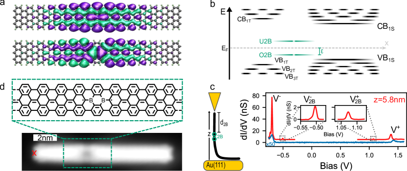
We performed two-terminal electronic transport measurements in GNRs suspended between the tip and a Au(111) substrate of a low-temperature scanning tunneling microscope (Koch et al., 2012; Friedrich et al., 2020, 2022) as sketched in Fig. 1c. To reach this configuration, the STM tip is positioned above one termination of the ribbon (e.g. over the red cross in Fig. 1d), and gently approached towards the substrate until a bond between tip and ribbon forms. Upon retracting the STM tip, the ribbon is partially lifted from the substrate, creating the two-terminal transport configuration. Since the ribbons are semiconducting, their linear conductance for small voltage biases drops exponentially with increasing tip-substrate-distance , with a decay constant that is characteristic of co-tunneling through the GNR band-gap (Koch et al., 2012).
To study the transport through a single 2B-dopant group, we retracted the ribbon to a tip height larger than , the spacing between the 2B site and GNR’s end. Close to , the detachment of the 2B moiety from the surface is detected in STS spectra as a faint Kondo resonance (Friedrich et al., 2020). A spectrum recorded above this point reveals two sharp peaks, and in Fig. 1d. They correspond to the onset of resonant band transport through the 7AGNR segments of the suspended ribbon as they are equally observed for a pristine 7AGNR lifted to a similar tip height (blue plot in Fig. 1d).
In the 2B-GNRs, we observed additional spectral features between the band transport resonances. For the ribbon in Fig. 1d, these in-gap features consist of two weaker peaks at and , shown in the figure’s inset. At the retraction height of , the 2B moiety lies in the free-standing segment of the ribbon and provides a exponentially localised state, which is decoupled from tip and substrate by the two pristine GNR segments and located in the ribbon’s band gap (as in Fig. 1b). In this configuration, electrical transport proceeds in a double-barrier fashion, where a fraction ( of the tip-substrate bias drops between tip and 2B-state, and the rest (1- between boron moiety and substrate, i.e., quantifies the electrostatic coupling. The position of the peaks in the spectra depends on the energy alignment of the 2B-states with respect to the chemical potential of the system ( and for the occupied and unoccupied state in Fig. 1b) and on the value of . Specifically, , and determine if the electrical transport is ambipolar (both O2B and U2B drive carriers at either polarity) or unipolar (resonant transport flow through only one of those states at either polarity) (Qiu et al., 2004; Nazin et al., 2005).
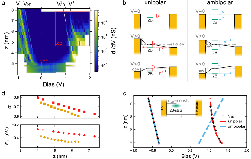
To decipher the transport mechanisms behind the two in-gap resonances, we modified by increasing the tip height, i.e. increasing the size of the 2B-substrate barrier, and studied changes in the spectra. In Fig. 2a, we plot a set of spectra recorded in the range as a color map that pictures the peak evolution with . The position of both peaks and shifts with towards more negative values, while their spacing is rather constant (see Supplementary Information (SI) for a detailed discussion). Note that the amplitude of is fairly constant during retraction, while decreases.
We modeled the -dependency of the position of both peaks by assuming that the fraction of potential drop scales with the ratio /, as in a parallel plate capacitor. Figure 2b details the conditions for resonant transport in the different transport configurations, which lead to analytical expressions for the -dependence of the and peaks (see SI for details). Using these expressions, we fitted in Fig. 2c the peak positions and from Fig. 2a with the ambipolar (blue line) and unipolar (red line) resonant transport model. Both models perfectly reproduce the -dependence of , which represents hole transport via the occupied 2B-state, i.e. the O2B+ resonance. However, the energy shift of the peak with is only reproduced in the case of unipolar transport, while the ambipolar behavior results in an opposite height dependence. The unipolar transport model even reproduces accurately a minute non-linearity observed only in the shift of . Therefore, we attribute both and peaks to unipolar hole transport through the O2B+ resonance, and discard resonant electron tunneling through the (negative ion) state U2B-.
The unipolar transport model also provides analytical expressions for the electrostatic coupling and the O2B+ hole resonance , with the elementary charge . We used these expressions to obtain the value of these two quantities at each value of from the experimental data available, without further assumptions (Fig. 2d). We find that decreases monotonously with increasing . This agrees with the continuous increase of the 2B-surface barrier width, which increases , as the tip retracts (Wagner et al., 2015). Accordingly, a second GNR with the 2B-unit closer to the tip by (orange symbols in Fig. 2d, refer to Fig. S2 for the conductance map) shows a similar decay of with but with a smaller value. Furthermore, the energy of the O2B+ hole resonance also shifts away from the Fermi level with increasing (Fig. 2d), from . We attribute the shift of to the reduction of the Au(111) surface-induced hole doping of the GNR (Merino-Díez et al., 2018) as the ribbon is lifted from the surface (Lawrence et al., 2020).
3 Current rectification
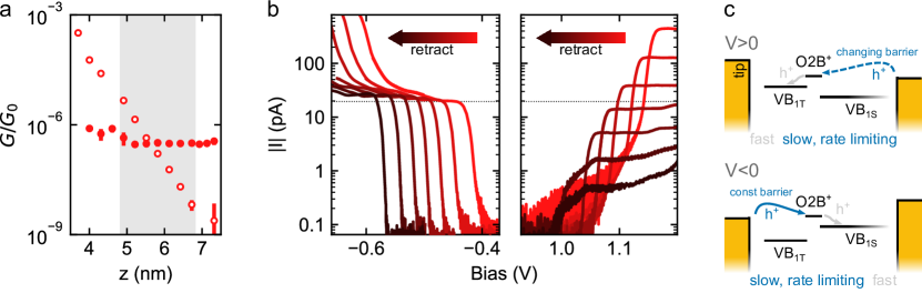
A striking feature of the conductance map in Fig. 2a is that, at negative voltage, the amplitude of O2B+ hole resonance remains rather constant during the whole retraction, even for separations as large as . However, the amplitude of the resonance at positive bias voltage decreases monotonously with . To quantify this, we compare in Fig. 3a the linear conductance of the resonances. The values of the negative bias conductance (filled circles) remain fairly constant during the whole tip retraction. On the other hand, decreases exponentially (open circles), and changes by six orders of magnitude during the 4 nm retraction, with decay constant . The ratio of resonant conductance (defined as resonant RR) changes by six orders of magnitude over the observed interval (from to ), showcasing a wide-range in-situ-tunability of the GNR’s diode character, exceeding other tunable devices (Batra et al., 2013; Perrin et al., 2016; Atesci et al., 2018). Notably, the forward bias direction reverses at . At this elevation the diboron unit lies around the midpoint of the tip-surface gap. The inversion of rectification direction has so far only been achieved by chemical modifications to the employed molecule (Nguyen et al., 2017), further evidencing our extraordinary ability of mechanical control over the rectification behaviour of the molecular device.
The corresponding current-bias-traces recorded in the range (Fig. 3b) reveal sharp current onsets upon reaching resonance conditions, followed by a constant current plateau. While for negative bias the current plateau amounts to independently of , at positive bias the current value is strongly sensitive to . A non-resonant RR, defined as RR, quantifies the diode character of the borylated GNR in an alternative way. A RR in the range of is reached at low bias voltage () and .
To rationalize the large current rectification in the unipolar transport via the 2B-state, we consider the tunneling channel opened by the O2B+ resonance (see Fig. 3c). As evidenced in Fig. 2, hole transport proceeds through the 2B-state when the positive-ion state O2B+ aligns with either tip’s () or substrate’s () chemical potential. At negative bias, hole tunneling from the tip is the rate-limiting process (blue arrow in Fig. 3c bottom), which remains constant with because the width of the tip-2B barrier is fixed. At positive bias, the rate-limiting step is hole tunneling from the substrate through the GNR barrier (blue arrow in Fig. 3c top), which increases with . Therefore, conductance at positive bias decreases exponentially as the ribbon is lifted. The presence of the two segments of GNR valence band at below the 2B-state reduces the apparent height of the barrier for hole tunneling and enables tunneling over large distances (Li et al., 2019; Lawrence et al., 2020). Additionally, a finite voltage drop across the 2B-state can alter the relative alignment of the two valence bands with respect to the O2B state, potentially lowering the height of the ”second” tunneling barrier further and, thus, facilitating the fast relaxation of the hole into the second electrode at either bias polarity (grey arrows in Fig. 3c).
Elevating the bias beyond resonant transport through the 2B-state enables resonant band transport at and . The peaks and , and the peaks and exhibit essentially identical energy shift with , evidencing that the band resonances found at higher bias correspond to unipolar resonant transport via the VB ( in Fig. 2a, see also SI for a detailed discussion). Most importantly, this enables efficient current rectification for bias voltage up to . The corresponding current plateau of at negative bias voltage is accessible over a large -interval and exhibits , exceeding values of reported molecular diodes (Chen et al., 2017b; Zhang et al., 2021).
4 Resonant phonon and quantum well states
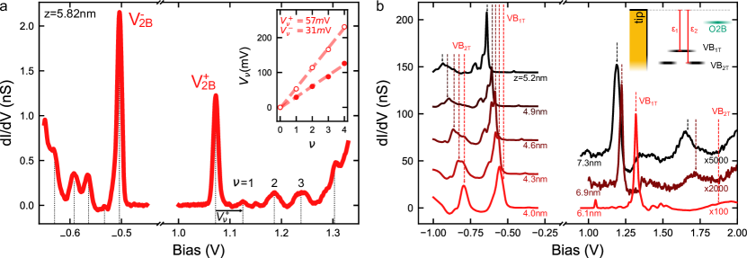
The peaks and are accompanied by a set of satellites (Fig. 4a) with equidistant energy spacing, which originate from unipolar resonant tunneling through vibronic states (Nazin et al., 2005; Franke and Pascual, 2012). The features show a characteristic amplitude pattern indicating that the same Franck-Condon coefficients govern the vibronic modes independent of the voltage polarity. Fitting the satellite peak’s energy by a linear regression (inset of Fig. 4a), we obtain the excitation energy at positive and negative bias.
The vibronic structure follows the same gating as the 2B-resonances. Therefore, we can apply the set of equations from the unipolar model discussed above to determine the fundamental vibrational energy and the corresponding for every . For example, we find that amounts to and at . We find that decays with tip retraction in a similar fashion as for the 2B-states, while remains constant with (see SI, Fig. S5). This excludes that corresponds to bending or torsional vibrations of the whole free standing segment. Instead, as we discuss in the SI (Fig. S5 and S6), these peaks most probably correspond to a vibrational mode of the boron moiety.
The confinement of the VB by the 2B-state gives rise to higher order quantum well modes inside the ribbon (Carbonell-Sanromà et al., 2017a) (Fig. 1b and inset Fig. 4b). Quantum well modes of 7AGNRs were spatially resolved by scanning tunneling spectroscopy (Söde et al., 2015; Carbonell-Sanromà et al., 2017a). The sharp transport resonances and , associated to the zero-order quantum well mode of the VB, are traced through a series of spectra of the 2B-GNR(VB in Fig. 4b). Using a simple particle-in-a-box model (see SI for details), we estimate the voltage at which the transport resonance corresponding to the second quantum well mode VB between tip and 2B-state is expected (Fig. 4b). Spectral resonances found above and in the spectra reproduce accurately the voltages obtained from the particle-in-a-box model confirming the access to quantum well modes of the confined VB via unipolar resonant transport.
5 Conclusion
We have demonstrated the unipolar resonant transport through a boron-induced in-gap state embedded in a 7AGNR suspended between two metallic electrodes. The state is available for hole transport at both voltage polarities. This transport channel was predicted to show a large degree of spin polarization (Zhang et al., 2022). The asymmetric position of the quantum dot in the ribbon enables a large in situ tunable current rectification (RR at ) likely following a mechanism comparable to current rectification in asymmetric two-level molecules (Elbing et al., 2005; Perrin et al., 2014, 2016). We are able to mechanically control the resonant RR by six orders of magnitude, including an inversion of forward bias direction. Furthermore, the presence of the boron moiety confines the valence band, creating quantum well states in the ribbon. We show that both ground and excited states of the quantized band are available for resonant electron transport. Our results extend the technological potential of atomically precise high-conductance graphene nanoribbons and shine light on a novel approach for the manipulation of molecular electronic functionalities.
6 Methods
The Au(111) substrate was prepared by sputtering the crystal with Neon ions for 10 minutes, followed by one annealing step at in ultra-high vacuum conditions () for 15 minutes. The ribbons were fabricated following the two-step on-surface synthesis via successive Ullmann-coupling and cyclodehydrogenation (Carbonell-Sanromà et al., 2017a, 2018; Friedrich et al., 2020). The samples are analyzed in situ in an homebuild STM kept with liquid Helium at . We use a PtIr tip. An atomically sharp apex termination by gold atoms was reached by controlled indention of the tip into the clean Au(111) substrate. Details on the lifting procedure to reach the two-terminal transport configuration are described in detail elsewhere (Friedrich et al., 2020). The experimental data was prepared for presentation using WSxM (Horcas et al., 2007) and the python matplotlib libary (Hunter, 2007). Colour maps use preceptual continuous colour scales based on (Kovesi, 2015).
References
- Aviram and Ratner (1974) A. Aviram and M. A. Ratner, Chemical physics letters 29, 277 (1974).
- Gupta et al. (2023) R. Gupta, J. A. Fereiro, A. Bayat, A. Pritam, M. Zharnikov, and P. C. Mondal, Nat. Rev. Chem. 7, 106 (2023).
- Yamada et al. (2008) R. Yamada, H. Kumazawa, T. Noutoshi, S. Tanaka, and H. Tada, Nano Lett. 8, 1237 (2008).
- Gehring et al. (2019) P. Gehring, J. M. Thijssen, and H. S. J. van der Zant, Nat. Rev. Phys. 1, 381 (2019).
- Chen et al. (2017a) X. Chen, M. Roemer, L. Yuan, W. Du, D. Thompson, E. Del Barco, and C. A. Nijhuis, Nature Nanotechnol. 12, 797 (2017a).
- Atesci et al. (2018) H. Atesci, V. Kaliginedi, J. A. Celis Gil, H. Ozawa, J. M. Thijssen, P. Broekmann, M.-a. Haga, and S. J. van der Molen, Nat. Nanotechnol. 13, 117 (2018).
- Batra et al. (2013) A. Batra, P. Darancet, Q. Chen, J. S. Meisner, J. R. Widawsky, J. B. Neaton, C. Nuckolls, and L. Venkataraman, Nano Lett. 13, 6233 (2013).
- Xin et al. (2017) N. Xin, J. Wang, C. Jia, Z. Liu, X. Zhang, C. Yu, M. Li, S. Wang, Y. Gong, H. Sun, G. Zhang, Z. Liu, G. Zhang, J. Liao, D. Zhang, and X. Guo, Nano Letters 17, 856 (2017).
- Nguyen et al. (2017) Q. v. Nguyen, P. Martin, D. Frath, M. L. Della Rocca, F. Lafolet, C. Barraud, P. Lafarge, V. Mukundan, D. James, R. L. McCreery, and J.-C. Lacroix, J. Am. Chem. Soc. 139, 11913 (2017).
- Yuan et al. (2015) L. Yuan, N. Nerngchamnong, L. Cao, H. Hamoudi, E. Del Barco, M. Roemer, R. K. Sriramula, D. Thompson, and C. A. Nijhuis, Nat. Commun. 6, 6324 (2015).
- Clair and de Oteyza (2019) S. Clair and D. G. de Oteyza, Chemical reviews 119, 4717 (2019).
- Cai et al. (2014) J. Cai, C. A. Pignedoli, L. Talirz, P. Ruffieux, H. Söde, L. Liang, V. Meunier, R. Berger, R. Li, X. Feng, K. Müllen, and R. Fasel, Nat. Nanotechnol. 9, 896 (2014).
- Chen et al. (2015) Y.-C. Chen, T. Cao, C. Chen, Z. Pedramrazi, D. Haberer, D. G. de Oteyza, F. R. Fischer, S. G. Louie, and M. F. Crommie, Nat. Nanotechnol. 10, 156 (2015).
- Carbonell-Sanromà et al. (2017a) E. Carbonell-Sanromà, P. Brandimarte, R. Balog, M. Corso, S. Kawai, A. Garcia-Lekue, S. Saito, S. Yamaguchi, E. Meyer, D. Sánchez-Portal, and J. I. Pascual, Nano Lett. 17, 50 (2017a).
- Rizzo et al. (2021) D. J. Rizzo, J. Jiang, D. Joshi, G. Veber, C. Bronner, R. A. Durr, P. H. Jacobse, T. Cao, A. Kalayjian, H. Rodriguez, P. Butler, T. Chen, S. G. Louie, F. R. Fischer, and M. F. Crommie, ACS Nano 15, 20633 (2021).
- Li et al. (2018) J. Li, N. Merino-Díez, E. Carbonell-Sanromà, M. Vilas-Varela, D. G. de Oteyza, D. Peña, M. Corso, and J. I. Pascual, Sci. Adv. 4, eaaq0582 (2018).
- Friedrich et al. (2022) N. Friedrich, R. E. Menchón, I. Pozo, J. Hieulle, A. Vegliante, J. Li, D. Sánchez-Portal, D. Peña, A. Garcia-Lekue, and J. I. Pascual, ACS Nano 16, 14819 (2022).
- Senkovskiy et al. (2017) B. V. Senkovskiy, M. Pfeiffer, S. K. Alavi, A. Bliesener, J. Zhu, S. Michel, A. V. Fedorov, R. German, D. Hertel, D. Haberer, L. Petaccia, F. R. Fischer, K. Meerholz, P. H. M. van Loosdrecht, K. Lindfors, and A. Grüneis, Nano Lett. 17, 4029 (2017).
- Chong et al. (2018) M. C. Chong, N. Afshar-Imani, F. Scheurer, C. Cardoso, A. Ferretti, D. Prezzi, and G. Schull, Nano Lett. 18, 175 (2018).
- Friedrich et al. (2020) N. Friedrich, P. Brandimarte, J. Li, S. Saito, S. Yamaguchi, I. Pozo, D. Peña, T. Frederiksen, A. Garcia-Lekue, D. Sánchez-Portal, and J. I. Pascual, Phys. Rev. Lett. 125, 146801 (2020).
- Carbonell-Sanromà et al. (2017b) E. Carbonell-Sanromà, J. Hieulle, M. Vilas-Varela, P. Brandimarte, M. Iraola, A. Barragán, J. Li, M. Abadia, M. Corso, D. Sánchez-Portal, D. Peña, and J. I. Pascual, ACS Nano 11, 7355 (2017b).
- Pei et al. (2022) T. Pei, J. O. Thomas, S. Sopp, M.-Y. Tsang, N. Dotti, J. Baugh, N. F. Chilton, S. Cardona-Serra, A. Gaita-Ariño, H. L. Anderson, and L. Bogani, Nature Communications 13, 4506 (2022).
- Niu et al. (2023) W. Niu, S. Sopp, A. Lodi, A. Gee, F. Kong, T. Pei, P. Gehring, J. Nägele, C. S. Lau, J. Ma, J. Liu, A. Narita, J. Mol, M. Burghard, K. Müllen, Y. Mai, X. Feng, and L. Bogani, Nature Materials 22, 180 (2023).
- Chen et al. (2023) Z. Chen, J.-R. Deng, S. Hou, X. Bian, J. L. Swett, Q. Wu, J. Baugh, L. Bogani, G. A. D. Briggs, J. A. Mol, C. J. Lambert, H. L. Anderson, and J. O. Thomas, Journal of the American Chemical Society 145, 15265 (2023).
- Zhang et al. (2023) J. Zhang, L. Qian, G. B. Barin, A. H. S. Daaoub, P. Chen, K. Müllen, S. Sangtarash, P. Ruffieux, R. Fasel, H. Sadeghi, J. Zhang, M. Calame, and M. L. Perrin, Nature electronics 6, 572 (2023).
- Lafferentz et al. (2009) L. Lafferentz, F. Ample, H. Yu, S. Hecht, C. Joachim, and L. Grill, Science 323, 1193 (2009).
- Koch et al. (2012) M. Koch, F. Ample, C. Joachim, and L. Grill, Nat. Nanotechnol. 7, 713 (2012).
- Jacobse et al. (2018) P. H. Jacobse, M. J. J. Mangnus, S. J. M. Zevenhuizen, and I. Swart, ACS Nano 12, 7048 (2018).
- Li et al. (2019) J. Li, N. Friedrich, N. Merino, D. G. de Oteyza, D. Peña, D. Jacob, and J. I. Pascual, Nano Lett. 19, 3288 (2019).
- Lawrence et al. (2020) J. Lawrence, P. Brandimarte, A. Berdonces-Layunta, M. S. G. Mohammed, A. Grewal, C. C. Leon, D. Sánchez-Portal, and D. G. de Oteyza, ACS Nano 14, 4499 (2020).
- Jiang et al. (2022) S. Jiang, F. Scheurer, Q. Sun, P. Ruffieux, X. Yao, A. Narita, K. Mullen, R. Fasel, T. Frederiksen, and G. Schull, “Length-independent quantum transport through topological band states of graphene nanoribbons,” (2022).
- Zhang et al. (2022) P. Zhang, X. Li, J. Dong, M. Zhu, F. Zheng, and J. Zhang, Appl. Phys. Lett. 120, 132406 (2022).
- Qiu et al. (2004) X. H. Qiu, G. V. Nazin, and W. Ho, Phys. Rev. Lett. 92, 206102 (2004).
- Nazin et al. (2005) G. V. Nazin, S. W. Wu, and W. Ho, PNAS 102, 8832 (2005).
- Wagner et al. (2015) C. Wagner, M. F. Green, P. Leinen, T. Deilmann, P. Krüger, M. Rohlfing, R. Temirov, and F. S. Tautz, Phys. Rev. Lett. 115, 1 (2015).
- Merino-Díez et al. (2018) N. Merino-Díez, J. Li, A. Garcia-Lekue, G. Vasseur, M. Vilas-Varela, E. Carbonell-Sanromà, M. Corso, J. E. Ortega, D. Peña, J. I. Pascual, and D. G. de Oteyza, J. Phys. Chem. Lett. 9, 25 (2018).
- Perrin et al. (2016) M. L. Perrin, E. Galán, R. Eelkema, J. M. Thijssen, F. Grozema, and H. S. van der Zant, Nanoscale 8, 8919 (2016).
- Franke and Pascual (2012) K. J. Franke and J. I. Pascual, J. Phys.: Condens. Matter 24, 394002 (2012).
- Chen et al. (2017b) X. Chen, M. Roemer, L. Yuan, W. Du, D. Thompson, E. del Barco, and C. A. Nijhuis, Nat. Nanotechnol. 12, 797 (2017b).
- Zhang et al. (2021) G.-P. Zhang, L.-Y. Chen, J.-M. Zhao, Y.-Z. Sun, N.-P. Shi, M.-L. Wang, G.-C. Hu, and C.-K. Wang, J. Phys. Chem. C 125, 20783 (2021).
- Söde et al. (2015) H. Söde, L. Talirz, O. Gröning, C. A. Pignedoli, R. Berger, X. Feng, K. Müllen, R. Fasel, and P. Ruffieux, Physical Review B - Condensed Matter and Materials Physics 91, 1 (2015).
- Elbing et al. (2005) M. Elbing, R. Ochs, M. Koentopp, M. Fischer, C. von Hänisch, F. Weigend, F. Evers, H. B. Weber, and M. Mayor, PNAS 102, 8815 (2005).
- Perrin et al. (2014) M. L. Perrin, R. Frisenda, M. Koole, J. S. Seldenthuis, J. A. C. Gil, H. Valkenier, J. C. Hummelen, N. Renaud, F. C. Grozema, J. M. Thijssen, D. Dulić, and H. S. J. van der Zant, Nat. Nanotechnol. 9, 830 (2014).
- Carbonell-Sanromà et al. (2018) E. Carbonell-Sanromà, A. Garcia-Lekue, M. Corso, G. Vasseur, P. Brandimarte, J. Lobo-Checa, D. G. de Oteyza, J. Li, S. Kawai, S. Saito, S. Yamaguchi, J. E. Ortega, D. Sánchez-Portal, and J. I. Pascual, J. Phys. Chem. C 122, 16092 (2018).
- Horcas et al. (2007) I. Horcas, R. Fernández, J. Gómez-Rodríguez, J. Colchero, J. Gómez-Herrero, and A. Baro, Rev. Sci. Instrum. 78, 013705 (2007).
- Hunter (2007) J. D. Hunter, Computing in Science and Engineering 9, 99 (2007).
- Kovesi (2015) P. Kovesi, “Good colour maps: how to design them,” (2015).
Acknowledgements
We gratefully acknowledge financial support from Spanish MCIN/AEI/ 10.13039/501100011033 and the European Regional Development Fund (ERDF) through grants with number PID2019-107338RBC6, PID2022-140845OB-C6, and CEX2020-001038-M, and from the European Union (EU) through Horizon 2020 (FET-Open project SPRING Grant. no. 863098).
Author information
Contributions
NF and JIP conceived the experiment. NF and JL performed the on-sufrace synthesis and STM/STS measurments. IP and DP synthesized the molecular precursors. NF analysed the experimental data and developed the theoretical model. NF, JL and JIP discussed the data and model. NF and JIP wrote the manuscript. All authors discussed and approved the manuscript.
7 Ethics Declaration
The authors declare no competing interests.