High-speed Readout System of X-ray CMOS Image Sensor for Time Domain Astronomy
Abstract
We developed an FPGA-based high-speed readout system for a complementary metal-oxide-semiconductor (CMOS) image sensor to observe soft X-ray transients in future satellite missions, such as HiZ-GUNDAM. Our previous research revealed that the CMOS image sensor has low-energy X-ray detection capability (0.4–4 keV) and strong radiation tolerance, which satisfies the requirements of the HiZ-GUNDAM mission. However, CMOS sensors typically have small pixel sizes (e.g., 10 ), resulting in large volumes of image data. GSENSE400BSI has 20482048 pixels, producing 6 Mbyte per frame. These large volumes of observed raw image data cannot be stored in a satellite bus system with a limited storage size. Therefore, only X-ray photon events must be extracted from the raw image data. Furthermore, the readout time of CMOS image sensors is approximately ten times faster than that of typical X-ray CCDs, requiring faster event extraction on a timescale of 0.1 s. To address these issues, we have developed an FPGA-based image signal processing system capable of high-speed X-ray event extraction onboard without storing raw image data. The developed compact system enabled mounting on a CubeSat mission, facilitating early in-orbit operation demonstration. Here, we present the design and results of the performance evaluation tests of the proposed FPGA-based readout system. Utilizing X-ray irradiation experiments, the results of the X-ray event extraction with the onboard and offline processing methods were consistent, validating the functionality of the proposed system.
1 Introduction
A future satellite mission, HiZ-GUNDAM [1], is being developed for time-domain astronomy, covering an energy band range of 0.4–4 keV. This mission has multiple payloads, including a wide-field X-ray monitor to detect X-ray transients such as gamma-ray bursts [2] and an infrared telescope specifically designed to perform follow-up observations of transients detected by the wide-field X-ray monitor [3]. Here, a wide-field X-ray monitor was designed with a field of view of str and sensitivity of for a 100-s exposure. The monitor also localizes the direction of the X-ray transients with a spatial resolution of 2 arcmin. Considering that the typical duration of gamma-ray bursts is 0.1–100 s [4], a photon-counting capability with a time resolution of 0.1 s is required.
The wide-field X-ray monitor was equipped with lobster eye optics [5, 6] to satisfy the wide field of view and high-sensitivity requirements and a focal pixel detector that can acquire the position and energy of incident X-ray photons. A back-illuminated complementary metal-oxide-semiconductor (CMOS) sensor [7] was positioned on the focal plane as an X-ray pixel detector. Our previous study confirmed that the CMOS sensor GSENSE400BSI-TVISB (Gpixel Inc., Table 1) [8, 9, 10, 11] is well-suited for mission requirements because of its low-energy X-ray detection capability, fast readout speed, and radiation tolerance [12].
Owing to the limitations of data storage onboard satellites, storing all the observed image data from CMOS sensors with an extremely large number of pixels (e.g., 2000 2000 pixels produces 6-Mbyte per frame for 12 bits) is impossible. Because the ratio of pixels with X-ray photon events to all pixels is less than 0.01%, a significant reduction in data size must be achieved by selectively extracting only X-ray events from the raw image data. Furthermore, this electronic readout system should be compact because of the limited space available on the satellite. Therefore, we developed a compact readout system dedicated to a CMOS sensor that performs X-ray event extraction and is suitable for satellite applications.
| Items | Parameters |
|---|---|
| Active image size | |
| Pixel size | |
| Number of pixels | |
| Max frame rate | 48 fps |
| Pixel clock rate | 25 MHz |
| Power consumption | 0.650 W |
2 Hardware Design and Functions
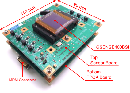
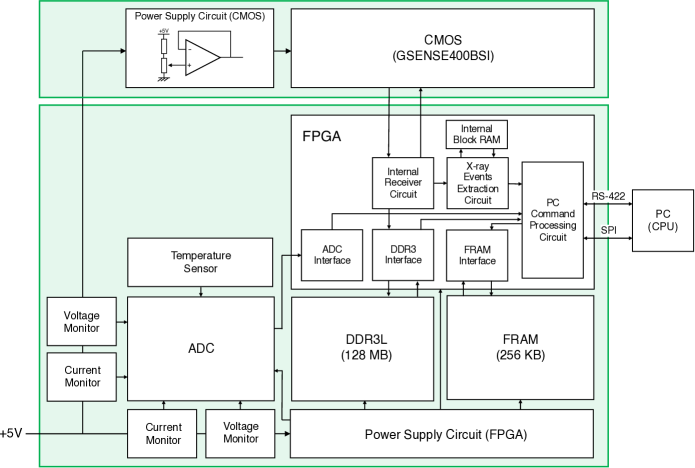
We adopted image processing utilizing a field-programmable gate array (FPGA) [13] to achieve high-speed synchronous image acquisition control from the CMOS sensors. The developed readout system comprises an FPGA board and a CMOS sensor board with stack structure and a compact size of 90 mm 110 mm 39 mm combined with the CMOS sensor (Figure 1). This system can be installed on middle-class satellites (e.g., HiZ-GUNDAM) and nanosatellites, such as the 6U CubeSat developed by the Tokyo Institute of Technology [14]. The FPGA board was equipped with a Xilinx Kintex-7 (XC7K325T-1FFG676I) with 400 I/Os [15] and an internal block RAM of 2MB [16], providing sufficient capabilities for controlling the CMOS sensor, reading out image data from the CMOS sensor, and extracting X-ray events from the raw image data, as mentioned in Sec. 3. This system operates with an external power supply of +5 V and outputs of +1.8 V, +3.3 V etc., utilized for digital ICs, including analog-to-digital converters (AD7928BRUZ, Analog Devices) and the FPGA.
We implemented the following three modes to be common for various observations with the CMOS sensor.
-
(1)
Frame mode: This mode outputs all the raw image data and is mainly employed for the optical and ultraviolet observations.
-
(2)
Event mode: This mode extracts only X-ray photon events from the observed image data and outputs their position, energy and time information, mainly utilized for X-ray photon-counting observations.
-
(3)
Housekeeping mode: In this mode, the housekeeping data of this system (e.g., the temperatures of the CMOS sensor and the FPGA board, the values of the voltage and current supplied to the CMOS and FPGA boards) are integrated as data packets and transferred to the bus system. This mode is adopted to monitor the system’s health status.
The system configuration of the developed readout board is illustrated in Figure 2. The FPGA board has two types of memory:128 MB DDR3L synchronous dynamic random access memory (SDRAM) [17] for storing raw image data from the CMOS sensor and 256 KB ferroelectric random access memory (FRAM) [18] for storing the configuration data of the CMOS sensor. The DDR3 memory functions as a buffer during operation in frame mode. Here, the power supply to the DDR3 memory can be turned off to reduce power consumption in event mode. FRAM, a type of nonvolatile memory that stores data utilizing ferroelectric polarization, is resistant to bit flipping caused by cosmic rays, known as single-event upset (SEU) [19]. Therefore, it stores critical operational settings for satellite missions, such as the CMOS setting data and threshold values required for extracting X-ray events that are not frequently rewritten. In orbit, for protection from bit flipping by the SEU, the setting data read from the FRAM are stored in three areas of the FPGA, and the majority decision is then applied.
This system incorporates two communication lines: the control line, which is utilized to send and receive commands such as changes in the operating mode, updating the configuration values, and sending back acknowledgments. Because high-speed data communication was not necessary for this line, RS-422 was adopted. The second is a data line, which transmits the frame and event data. Because the data line requires faster communication than the control line, an SPI communication of a few megabytes per second was utilized.
3 X-ray Event Extraction utilizing FPGA
This section describes the procedure for the X-ray event extraction implemented in the FPGA. Upon the interaction of X-rays with the CMOS sensor, X-ray events can be divided into two pixel patterns: "single-pixel" and "multi-pixel" [12], because signals on the pixels from an X-ray photon are often distributed within a single pixel and multi-pixels. In the case of multi-pixel events, the correct energy information for an incident X-ray photon can be obtained by summing the pixel values.
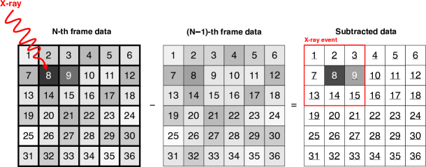
We first describe the event extraction procedure performed utilizing offline software. For simplicity, we consider a CMOS sensor with a 66 pixel area. To process the image data and identify X-ray events with photon energies and positions, we adopted the following method in the offline software (Figure 3):
-
(1)
In the image data output from the CMOS sensor, each pixel has an offset voltage. This voltage varies for each pixel owing to the CMOS fabrication processes. Thus, for obtaining X-ray photon energy accurately and efficiently, it is essential to subtract the consecutive pixel images, e.g., subtraction between the 2nd and 1st images, 3rd and 2nd images, 4th and 3rd images, and so forth.
-
(2)
We adopted two types of threshold to detect only the X-ray photon events efficiently: an "event threshold" to identify a primary pixel which mainly interacted with an X-ray photon and a "split threshold" to collect signals from the adjacent 33 pixels around the primary pixel for the multi-pixel events.
-
(3)
Pixels with analog-to-digital-unit (ADU) values above the event threshold are identified as X-ray events.
-
(4)
If the signals from any adjacent pixel do not exceed the split threshold, the event is labeled as a single-pixel event. Otherwise, the event is categorized as a multi-pixel event, and all ADU values exceeding the two thresholds in the 33 pixels are summed up to derive the X-ray photon energy.
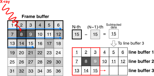
The following procedure was implemented on the FPGA. The schematic procedure of the FPGA-based real-time event processing is illustrated in Figure 4. Here, owing to the limitation of the size of the internal block RAM of the FPGA, two-frame buffers for storing two raw image datasets cannot be implemented. Instead, we utilized a one-frame buffer to store two raw image data points and three line buffers with a small RAM size for subtracting two images (see below for details). The numbers in the frame buffer in Figure 4 depict the pixel IDs, and the sensor outputs data in order from the 1st to the 36th pixel.
-
(1)
Figure 4 presents just one example with subtraction of pixel ID 15 to illustrate the procedure. First, the -th image data is stored in pixel IDs 1–14, and the -th image data is stored in pixel IDs 15–36, as illustrated in Figure 4. When the ADU value with pixel ID 15 is taken from the sensor, the system subtracts the -th data stored in the frame buffer from the ADU value taken from the sensor with pixel ID 15, and the subtracted ADU value is obtained.
-
(2)
After subtracting pixel ID 15, the ADU value of pixel 15 in the frame buffer is updated to the ADU value taken from the sensor.
-
(3)
The subtracted data is stored in the line buffer. Then, the system performs pixel pattern matching with 33 pixel data for X-ray event extraction. Here, we follow the pattern matching developed by ASCA/SIS of the previous astronomical satellite [20].
-
(4)
By repeating steps (1)–(3), event extraction of all image data can be performed. Here, if the three line buffers are filled at pixel ID 18, a new pixel value of pixel ID 19 is stored at the starting point of the line buffer 1. The same procedure is performed subsequently but with a modified pixel pattern due to a different row position.
In the next section, we present the results of system performance verification employing the two methods.
4 Performance verification
To confirm that the system with the implemented functions functioned properly, the following two experiments were performed:
-
(1)
Real-time detection and event extraction with an exposure time of 0.1 s by mimicking a transient X-ray phenomenon utilizing a radioactive source.
-
(2)
Comparison of spectra obtained by the offline and onboard processing methods and consistency verification between them.
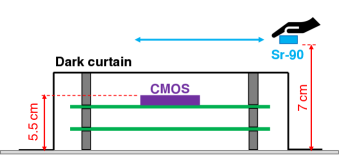
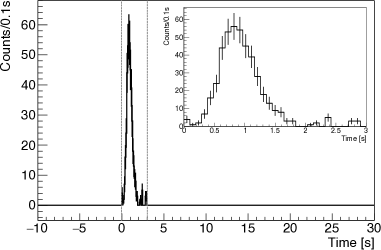
For the first experiment, we utilized -rays emitted from Sr-90 with Bq in the air to mimic an X-ray transient event with a timescale of 1 s. Because of low radioactivity, mimicking a clear X-ray pulse utilizing X-ray radioactive sources was difficult. Sr-90 beta decays to Y-90 with a half-life of 28.79 years, emitting a maximum of 546 keV -rays. Y-90 beta decays to Zr-90 with a half-life of 64 h, emitting a maximum of 2.28 MeV -rays [21]. -rays emitted by these decay processes enter the CMOS sensor and deposit energies of 4 keV. The deposited energy is almost equivalent to the target X-ray energy band of HiZ-GUNDAM. Note that 99% of -ray events are multi-pixel events. Figure 5(a) illustrates the experimental setup. The CMOS sensor and the developed readout system were covered with a dark curtain. Subsequently, a light curve measured every 0.1 s was obtained by moving Sr-90 quickly over the CMOS sensor. Figure 5(b) presents the measured light curve obtained utilizing the onboard detection method. This result indicates that a clear spike was detected with a timescale of 1 s and that the FPGA-based event processing worked correctly.
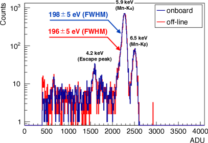
In the second experiment, we measured the 5.9 keV (Mn-Kα) and 6.5 keV (Mn-Kβ) lines from Fe-55 adopting this system. Figure 6 illustrates the spectra obtained utilizing offline and onboard methods for an Fe-55 source at 20 ∘C. The X-ray fluorescence lines at 5.9 keV and 6.5 keV from Fe-55 and Si escape line of Mn-Kα (4.2 keV) were clearly detected. Furthermore, the two measured spectra obtained via the two methods were identical within statistical uncertainty. The measured energy resolutions at 5.9 keV (full width at half maximum, FWHM) were 1965 eV utilizing the offline method, and 1985 eV the onboard method. This result confirms that there is no significant noise contribution due to the different processing methods and that the onboard acquisition system can obtain accurate X-ray energy information without increasing noise.
Note that the power consumption of the FPGA for the two experiments was measured to be approximately 3 W, except for the CMOS sensor.
5 Conclusion
We developed a CMOS image-sensor readout system for future satellite missions HiZ-GUNDAM. This system has a stacking structure comprising a CMOS sensor and FPGA boards with a compact size that can be mounted on the 2U-CubeSat. Adopting an FPGA-based X-ray event-extraction system, the light curve and spectrum were successfully measured in real time without significant performance degradation. Our results demonstrate that the developed high-speed readout system works well and applies to future satellite missions.
Acknowledgments
This study was supported by JSPS KAKENHI Grant Numbers JP17H06362 (M.A.), JP22J12717 (N.O.), JP23H04898 (M.A. and D.Y.), JP23H04895 (T. Sawano and T. Sakamoto), the CHOZEN Project of Kanazawa University (M.A., T. Sawano, and D.Y.), and the JSPS Leading Initiative for Excellent Young Researchers Program (M.A.).
References
- [1] Daisuke Yonetoku et al. High-redshift gamma-ray burst for unraveling the Dark Ages Mission: HiZ-GUNDAM. SPIE Conference Series, 2020.
- [2] Ray W. Klebesadel et al. Observations of Gamma-Ray Bursts of Cosmic Origin. ApJ, 1973.
- [3] Kohji Tsumura et al. Development of an optical and near-infrared telescope onboard the HiZ-GUNDAM mission. SPIE Conference Series, 2020.
- [4] Charles A. Meegan et al. The Third BATSE Gamma-Ray Burst Catalog. ApJS, 1996.
- [5] J. R. P. Angel. Lobster eyes as X-ray telescopes. ApJ, 1979.
- [6] Hatsune Goto et al. Development of a method for aligning lobster eye optics onboard HiZ-GUNDAM with visible light and shape measurements. SPIE Conference Series, 2022.
- [7] E. R. Fossum. CMOS image sensors: electronic camera-on-a-chip. IEEE Transactions on Electron Devices, 1997.
- [8] Cheng Ma et al. A 4MP high-dynamic-range, low-noise CMOS image sensor. SPIE Conference Series, 2015.
- [9] Wenxin Wang et al. Developments of scientific CMOS as focal plane detector for Einstein Probe mission. SPIE Conference Series, 2018.
- [10] Tetsuo Harada et al. Energy- and spatial-resolved detection using a backside-illuminated CMOS sensor in the soft X-ray region. Applied Physics Express, 2019.
- [11] Noriyuki Narukage et al. High-speed back-illuminated CMOS sensor for photon-counting-type imaging-spectroscopy in the soft X-ray range. NIM-A, 2020.
- [12] Naoki Ogino et al. Performance verification of next-generation Si CMOS soft X-ray detector for space applications. NIM-A, 2021.
- [13] Stephen Brown and Jonathan Rose. FPGA and CPLD architectures: A tutorial. IEEE design & test of computers, 1996.
- [14] Yoichi Yatsu et al. Conceptual design of a wide-field near UV transient survey in a 6U CubeSat. In Space Telescopes and Instrumentation 2018: Ultraviolet to Gamma Ray, 2018.
- [15] Xilinx Inc. 7 Series FPGAs Packaging and Pinout Product Specification User Guide (UG475, v1.19). https://docs.xilinx.com/v/u/en-US/ug475_7Series_Pkg_Pinout, 2021.
- [16] Xilinx Inc. 7 Series FPGAs Data Sheet: Overview (DS180, v2.6.1). https://docs.xilinx.com/v/u/en-US/ds180_7Series_Overview, 2020.
- [17] HA Nikel et al. DDR-SDRAM, high-speed, source-synchronous interfaces create design challenges. EDN, 1999.
- [18] Hiroshi Ishiwara. Ferroelectric random access memories. Journal of nanoscience and nanotechnology, 2012.
- [19] Michael Nicolaidis. Design for soft error mitigation. IEEE Transactions on Device and Materials Reliability, 2005.
- [20] B.E. Burke et al. CCD soft x-ray imaging spectrometer for the ASCA satellite. IEEE Transactions on Nuclear Science, 1994.
- [21] H.H. Hansen. Measurement of the beta-ray spectra of 90Sr-90Y. The International Journal of Applied Radiation and Isotopes, 1983.