Detecting the Néel vector of altermagnet by attaching a
topological insulator
and crystalline valley-edge insulator
Abstract
In order to detect the Néel vector of an altermagnet, we investigate topological phases in a bilayer system composed of an altermagnet and a two-dimensional topological insulator described by the Bernevig-Hughes-Zhang model. A topological phase transition occurs from a first-order topological insulator to a trivial insulator at a certain critical altermagnetization if the Néel vector of altermagnet is along the axis or the axis. It is intriguing that valley-protected edge states emerge along the Néel vector in this trivial insulator, which are as stable as the topological edge states. We name it a crystalline valley-edge insulator. On the other hand, the system turns out to be a second-order topological insulator when the Néel vector is along the axis. The tunneling conductance has a strong dependence on the Néel vector. In addition, the band gap depends on the Néel vector, which is measurable by optical absorption. Hence, it is possible experimentally to detect the Néel vector by measuring tunneling conductance and optical absorption.
Ferromagnets and antiferromagnets are typical examples of magnets. On one hand, ferromagnets are used for magnetic memory, where the direction of magnetization stores the nonvolatile memory. The magnetization direction can be read out electrically by using the anomalous Hall effect due to the time-reversal breaking. However, ferromagnets produce stray field due to the nonzero net magnetization, which prevents ultra high density integrated memory. On the other hand, antiferromagnet spintronics[1, 2, 3, 4, 5, 6, 7] have a merit that it is possible to make ultra high density integrated memory due to the zero net magnetization. In addition, the flipping speed of antiferromagnets is much faster than that of ferromagnets[8]. However, it is very hard to read out the Néel vector because the anomalous Hall effect is absent due to the combination symmetry of time-reversal symmetry and translational symmetry. One of the solution is multipolar antiferromagnet[9], where the anomalous Hall effect is observed.
Recently, altermagnets have attracted rapid growth of interest[10, 11, 12]. It is the third-type of magnets in terms of symmetry. Altermagnets break time-reversal symmetry. Hence, an anomalous Hall effect emerges[13, 14, 15, 16], which can be used for readout of the component of altermagnetization. Furthermore, there is no net magnetization in altermagnets, which may lead to an ultra-high density integration and high flipping rate of memory. Namely, altermagnets have merits of both ferromagnets and antiferromagnets. The characteristic feature of altermagnets is a momentum-dependent band structure for each spin [10, 11, 12]. Indeed, momentum dependent band structures are observed by Angle-Resolved Photo-Emission Spectroscopy (ARPES)[17, 18, 19, 20, 21]. Furthermore, spin current is generated by applying electric field[22, 23, 24, 25] owing to the above-mentioned characteristic band structure. There are only few works on topological properties[26] induced by altermagnets except for Majorana states[27, 28, 29].
In this paper, analyzing a bilayer system composed of an altermagnet and a two-dimensional topological insulator, we construct a topological phase diagram. It has intriguing features. On one hand, a topological phase transition occurs from a first-order topological insulator to a trivial insulator at a certain altermagnetization when the Néel vector is along the axis or the axis. This trivial insulator is intriguing since it is characterized by the emergence of edge states parallel to the Néel vector, which are as robust as topological edges. Furthermore, an edge state connects two valleys either in the occupied band or in the unoccupied band, as is a reminiscence of the valley-protected edge states in the valley-Chern insulator[30]. Hence, we name it the -axis crystalline valley-edge insulator (-CVEI) or the -axis crystalline valley-edge insulator (-CVEI). On the other hand, the system becomes a second-order topological insulator (SOTI) when the Néel vector is along the axis. We show that tunneling conductance has a sharp dependence on the Néel vector. In addition, the band gap has a dependence on the Néel vector, which is measured by optical absorption. Therefore, the Néel vector is experimentally determined by combining the tunneling conductance and the optical absorption spectra.
Model: We analyze the bilayer system where -wave altermagnet is attached on a two-dimensional topological insulator. The Hamiltonian is given by
| (1) |
The topological insulator is described by the Bernevig-Hughes-Zhang (BHZ) model[31],
| (2) |
with , where is the mass parameter, is the hopping parameter, is the spin-orbit interaction, is the Pauli matrix for the spin and is the Pauli matrix for the orbital. The BHZ model describes a topological insulator for .
The effect of -wave altermagnet is described by the Hamiltonian[10, 11, 12, 27, 29, 28]
| (3) |
with , where is the magnitude of altermagnetization and is the Néel vector. The Néel vector is controlled by spin-orbit torque[32, 33] or spin-split torque[34, 35]. The characteristic feature of altermagnet is that the magnetization has a momentum dependence as in the Hamiltonian (3).
Band gap: We study the bulk band gap. If the Néel vector is along the axis, the energy spectrum is given by
| (4) |
The minimum of the band gap is taken at . The solution is . The gap closing condition is
| (5) |
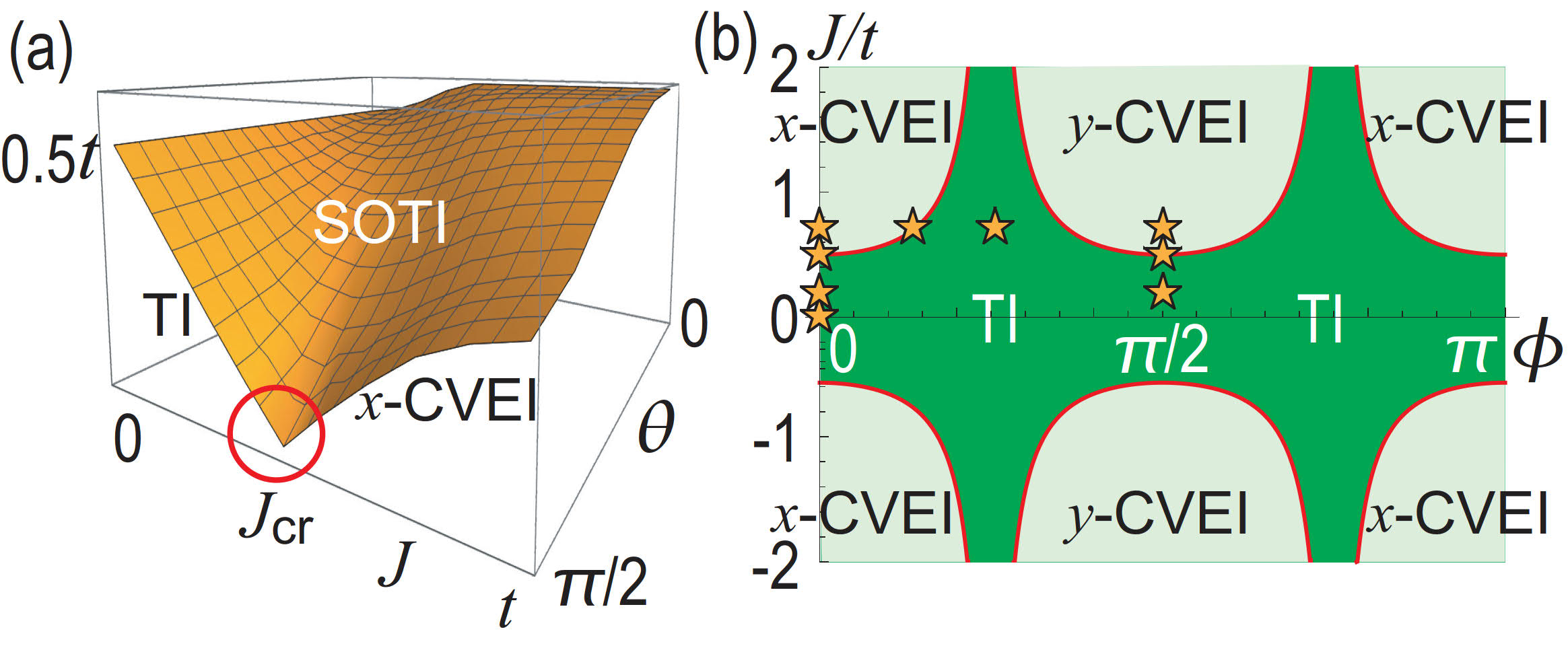
We show the band gap in the - plane at in Fig.1(a). The band gap closes at when .
If the Néel vector is in the - plane with angle , the energy spectrum is given by
| (6) | |||||
The bulk band gap closes at with
| (7) |
and . We have shown the gap-closing curves in Fig.1(b). We later argue that they are topological phase boundaries when the Néel vector is within the - plane.
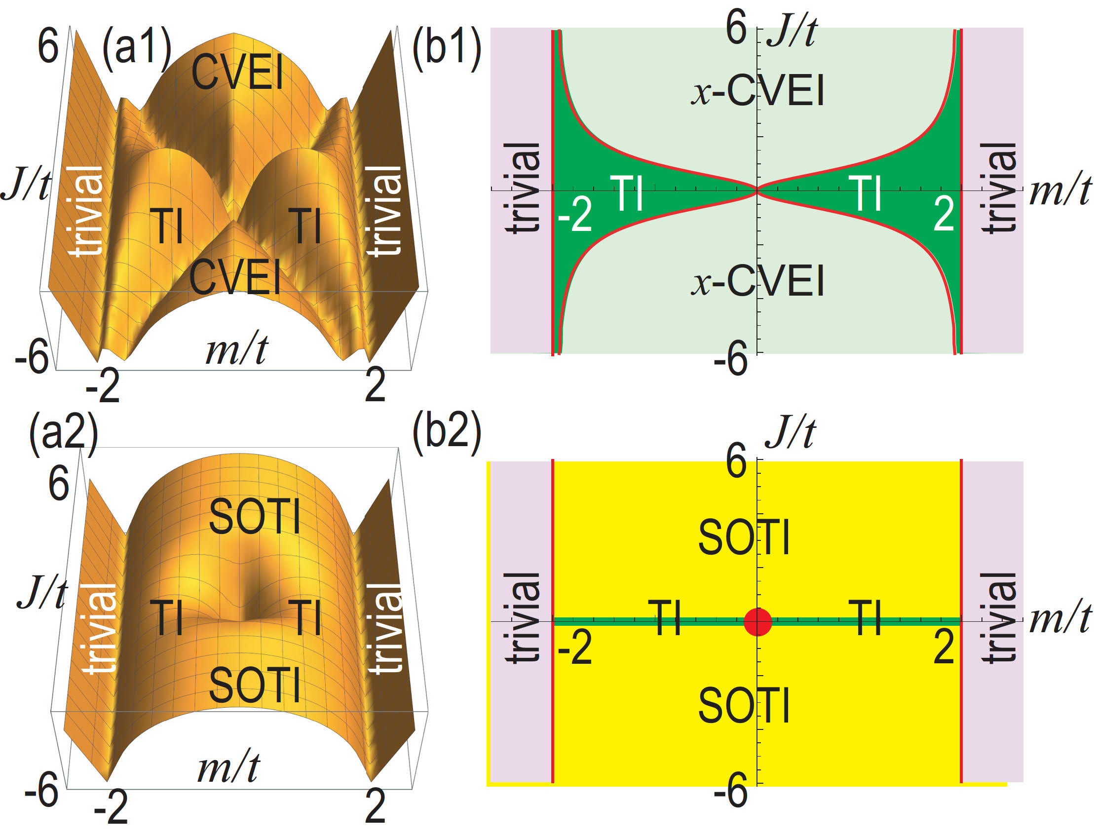
We show the band-gap structure in the - plane when the Néel vector is along the -axis in Fig.2(a1) and the gap-closing curves in Fig.2(b1). We later argue that they are topological phase boundaries. The trivial phase of the BHZ model remains as it is for and 0. However, a new type of trivial insulator emerge for and , as described below.
If the Néel vector is along the axis (), the energy spectrum is given by
| (8) |
The band gap is shown in Fig.2(a2). It implies that the altermagnetization does not contribute to the gap closing and the gap closing condition is identical to that of the BHZ model, i.e., as in Fig.2(b2). Hence, the topological phase boundaries remain the same as those of the BHZ model. However, the topological phase is changed from the first-order one to the second-order one, as described below.
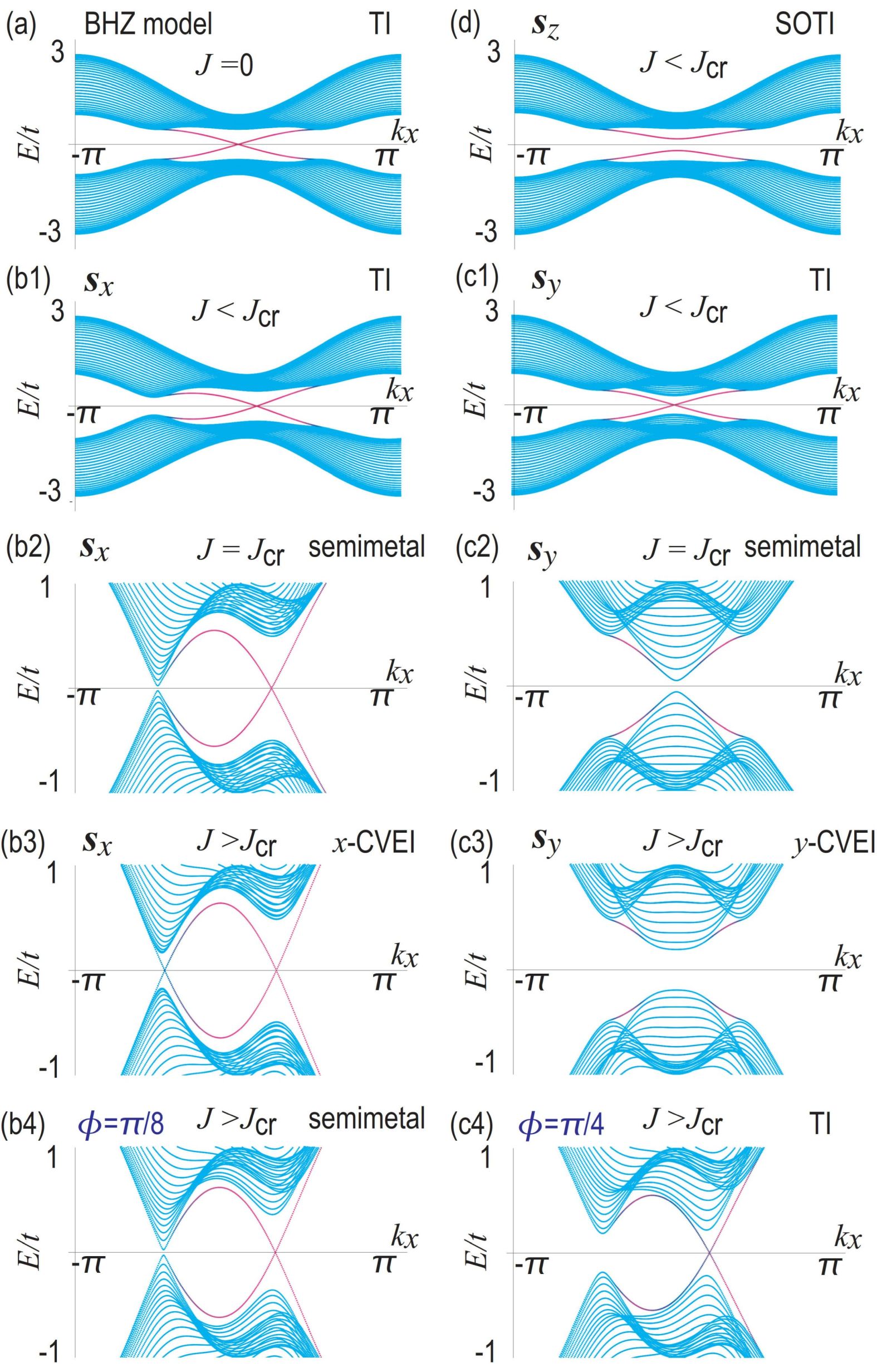
Ribbon geometry: We analyze the energy spectrum of the total Hamiltonian with ribbon geometry to see the topological property. In the absence of the altermagnetization, , there are topological edge states of the BHZ model (2), which cross at the momentum , as in Fig.3(a).
If the altermagnetization is along the axis, , the crossing point of the topological edge states moves away from for as in Fig.3(b1). At the critical point , the bulk band gap closes and the system is a semimetal as in Fig.3(b2). For , each edge state connects either the occupied band or the unoccupied band, as in Fig.3(b3). It indicates the system is trivial. Although the edge states are nontopological, they are robust against the order of the band gap because the turning point of the edge state much exceeds the band gap. Indeed, it requires perturbation much larger than the band gap to remove the trivial edge states. These nontopological edge states are as robust as topological edges. They are a reminiscence of the valley-protected edge states with each edge connecting two valleys either in the occupied band or in the unoccupied band[30].
If the altermagnetization is along the axis, , the topological edge states are maintained for as in Fig.3(c1). At the critical point , the bulk band gap closes as in Fig.3(c2). Edge states disappear for as in Fig.3(c3).
We show the band structure when the altermagnetization is given by for the cases , in Fig.3(b4), (c4), respectively. The bulk band gap closes in the vicinity of as in Fig.3(b4) and Fig.1(b). The valley-protected edge states become the topological edge states as in Fig.3(c4) and Fig.1(b).
If the altermagnetization is along the axis, , the topological edge states anticross and a finite gap emerges in edge states as in Fig.3(d). It means that the system is not a first-order topological insulator. We will soon see that the system is a second-order topological insulator, which is characterized by the emergence of corner states in square geometry.
Square geometry: We investigate the energy spectrum of the total Hamiltonian with square geometry to see the topological property more in detail.
In the case of or , the edge states emerge along the axis or the axis, as in Fig.4(a1) or (a2), respectively. Correspondingly, the energy spectrum is linear as a function of the eigenindex in the vicinity of the zero energy, as in Fig.4(b1) or (b2). These edge states are nontopological as we have argued in ribbon geometry. On the other hand, there are no edge states along the axis or the axis in the case of or as in Fig.4(a1) or (a2), respectively. It is a reminiscence of edge states of topological crystalline insulator[36]. The system is the -axis crystalline valley-edge insulator (-CVEI) in Fig.4(a1) and the -axis crystalline valley-edge insulator (-CVEI) in Fig.4(a2).
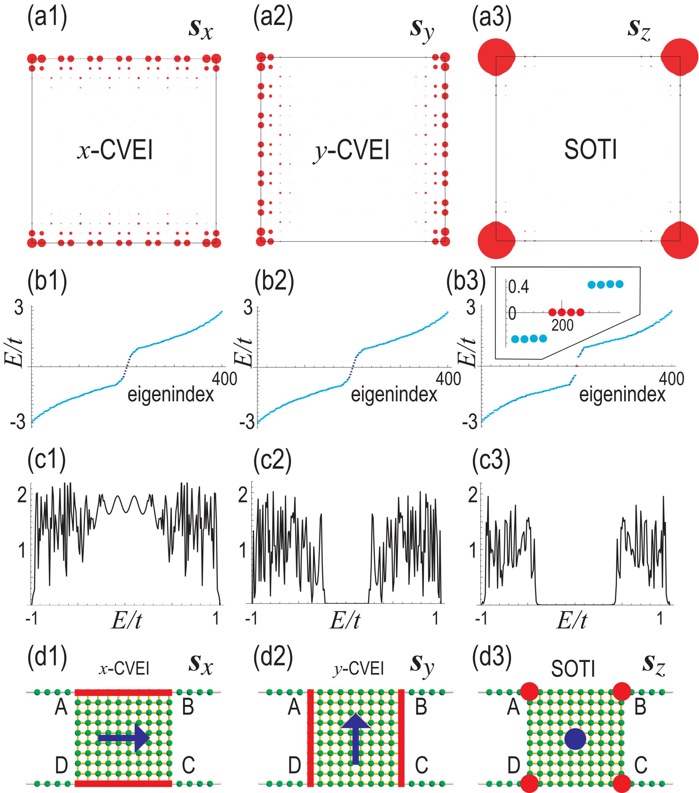
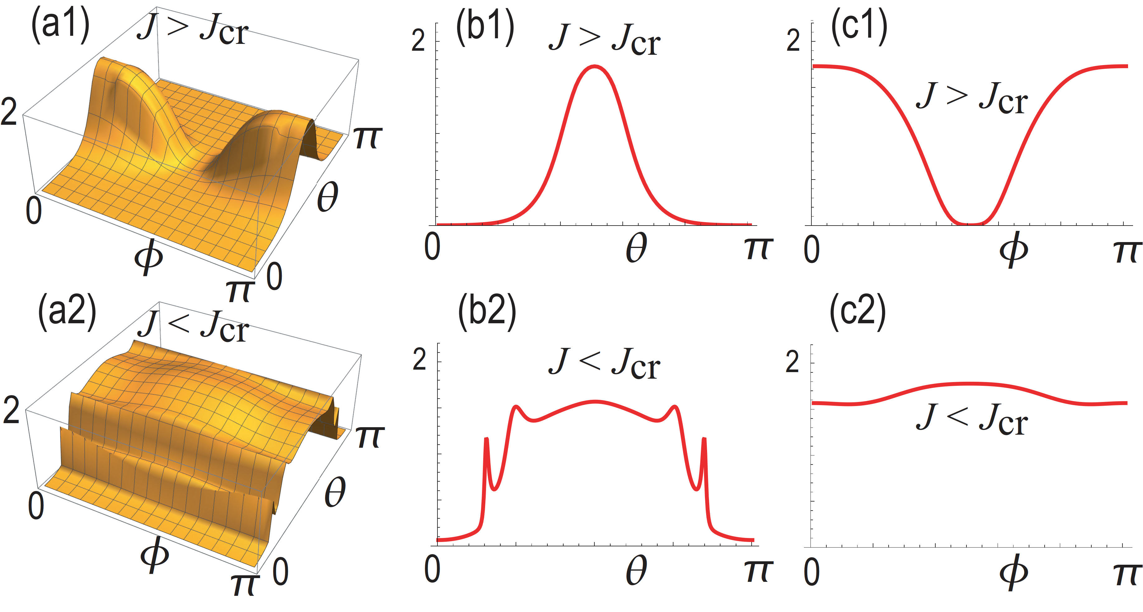
In the case of , four topological corner states emerge as in Fig.4(a3). Correspondingly, there are four zero-energy corner states within a finite gap as in Fig.4(b3). As a result, the system is a second-order topological insulator.
Conductance: We show that the Néel vector is detectable by measuring the conductance in the setup shown in Fig.4(d1)(d3), where four leads are attached to the corners of the square sample. We assume that the leads are single-atomic chains with semi-infinite length.
The conductance between two leads is calculated based on the Landauer formalism[37, 38, 39, 40, 41]. The conductance at energy is calculated as[37]
| (9) |
where is the line width with the self-energies and for the left and right leads, and is the Green function with the Hamiltonian for the sample. The self energy of a single-atomic semi-infinite chain is analytically obtained[37] as .
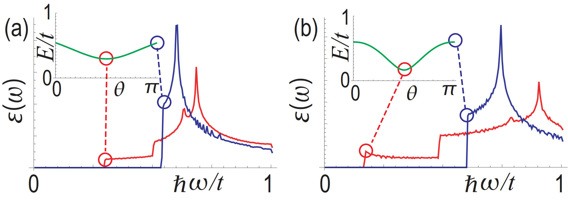
First, we study the case . We show the conductance as a function of the energy in Fig.4(c1), (c2) and (c3). We have calculated the conductance between the leads A and B. The conductance is nonzero at when the Néel vector is along the axis as in Fig.4(c1). It is understood that the current flows through the edge state along the axis as in Fig.4(d1). On the other hand, it is zero at when the Néel vector is along the axis as in Fig.4(c2). It is because there is no edge state to carry the current along the axis as in Fig.4(d2). The conductance is also zero at when the Néel vector is along the axis as in Fig.4(c3). It is because there is no edge state although corner states exist as in Fig.4(d3). It seems to be difficult to differentiate the cases where the Néel vector is along the axis or the axis by measuring the conductance because the tunneling conductance is zero for both cases. However, it is differentiated by mearing the tunneling conductance between the leads A and D, where the conductance is nonzero if the Néel vector is along the axis but zero if the Néel vector is along the axis.
The conductance in the - plane is shown in Fig.5(a1). The conductance as a function of at is shown in Fig.5(b1). The conductance takes maximum value at and takes minimum value at . The conductance as a function of at is shown in Fig.5(c1). The conductance takes the maximum value at and the minimum value at . Hence, we can detect the Néel vector by measuring the conductance.
Next, we study the case . We show the conductance in the - plane in Fig.5(a2). The dependence on the angle is tiny comparing with the case , as in Fig.5(c2). It is because the system is a first-order topological insulator, where the topological edge state surround the sample. The conductance is zero for and as in the case of the system , as in Fig.5(b2). It is because there are topological corner states but there are no edge states.
Optical absorption: We show that the band gap is observed by examining the optical absorption spectrum. We analyze the optical inter-band transition from the state in the valence band to the state in the conduction band. We apply a circularly polarized light, where the electromagnetic potential is given by .
The optical absorption is calculated based on the Kubo formula[42, 43, 44, 45, 36],
| (10) |
where is the optical matrix element , and are the energies of the conduction and valence bands, and is the Fermi distribution function.
We show the optical absorption spectra at and in Fig.6. There is a gap in the spectrum, implying the sudden occurrence of the optical absorption at the moment that the photon energy becomes the same as the band-gap energy. Hence, the band gap is measured by optical absorption experiments.
In conclusion, it is possible to determine the Néel vector by measuring the tunneling conductance and the optical absorption.
The author is very much grateful to S. Seki for helpful discussions on the subject. This work is supported by CREST, JST (Grants No. JPMJCR20T2) and Grants-in-Aid for Scientific Research from MEXT KAKENHI (Grant No. 23H00171).
References
- [1] T. Jungwirth, X. Marti, P. Wadley and J. Wunderlich, Antiferromagnetic spintronics, Nature Nanotechnology 11, 231 (2016).
- [2] V. Baltz, A. Manchon, M. Tsoi, T. Moriyama, T. Ono, and Y. Tserkovnyak Antiferromagnetic spintronics, Rev. Mod. Phys. 90, 015005 (2018).
- [3] Jiahao Han, Ran Cheng, Luqiao Liu, Hideo Ohno and Shunsuke Fukami, Coherent antiferromagnetic spintronics Nature Materials 22, 684 (2023).
- [4] Zhuoliang Ni, A. V. Haglund, H. Wang, B. Xu, C. Bernhard, D. G. Mandrus, X. Qian, E. J. Mele, C. L. Kane and Liang Wu , Imaging the Neel vector switching in the monolayer antiferromagnet MnPSe3 with strain-controlled Ising order Nature Nanotechnology 16, 782 (2021).
- [5] J. Godinho, H. Reichlov, D. Kriegner, V. Novak, K. Olejnik, Z. Kašpar, Z. Šoban, P. Wadley, R. P. Campion, R. M. Otxoa, P. E. Roy, J. Železnny, T. Jungwirth and J. Wunderlich, Electrically induced and detected Neel vector reversal in a collinear antiferromagnet, Nature Communications volume 9, Article number: 4686 (2018).
- [6] Kenta Kimura, Yutaro Otake and Tsuyoshi Kimura, Visualizing rotation and reversal of the Neel vector through antiferromagnetic trichroism, Nature Communications, 13, 697 (2022).
- [7] Yi-Hui Zhang, Tsao-Chi Chuang, Danru Qu, and Ssu-Yen Huang, Detection and manipulation of the antiferromagnetic Neel vector in Cr2O3 Phys. Rev. B 105, 094442 (2022).
- [8] Hao Wu, Hantao Zhang, Baomin Wang, Felix Gro, Chao-Yao Yang, Gengfei Li, Chenyang Guo, Haoran He, Kin Wong, Di Wu, Xiufeng Han, Chih-Huang Lai, Joachim Gre, Ran Cheng and Kang L. Wang, Current-induced Neel order switching facilitated by magnetic phase transition, Nature Communications 13, 1629 (2022).
- [9] Satoru Nakatsuji, Naoki Kiyohara and Tomoya Higo, Large anomalous Hall effect in a non-collinear antiferromagnet at room temperature, Nature 527, 212 (2015).
- [10] L. Smejkal, A. H. MacDonald, J. Sinova, S. Nakatsuji and T. Jungwirth, Anomalous Hall antiferromagnets, Nat. Rev. Mater. 7, 482 (2022).
- [11] L. Smejkal, J. Sinova, and T. Jungwirth, Beyond Conventional Ferromagnetism and Antiferromagnetism: A Phase with Nonrelativistic Spin and Crystal Rotation Symmetry, Phys. Rev. X, 12, 031042 (2022).
- [12] Libor Šmejkal, Jairo Sinova, and Tomas Jungwirth, Emerging Research Landscape of Altermagnetism, Phys. Rev. X 12, 040501 (2022).
- [13] Amar Fakhredine, Raghottam M. Sattigeri, Giuseppe Cuono, and Carmine Autieri, Interplay between altermagnetism and nonsymmorphic symmetries generating large anomalous Hall conductivity by semi-Dirac points induced anticrossings, Phys. Rev. B 108, 115138 (2023).
- [14] Teresa Tschirner, Philipp Keler, Ruben Dario Gonzalez Betancourt, Tommy Kotte, Dominik Kriegner, Bernd Buechner, Joseph Dufouleur, Martin Kamp, Vedran Jovic, Libor Smejkal, Jairo Sinova, Ralph Claessen, Tomas Jungwirth, Simon Moser, Helena Reichlova, Louis Veyrat, Saturation of the anomalous Hall effect at high magnetic fields in altermagnetic RuO2, arXiv:2309.00568
- [15] Toshihiro Sato, Sonia Haddad, Ion Cosma Fulga, Fakher F. Assaad, Jeroen van den Brink, Altermagnetic anomalous Hall effect emerging from electronic correlations, arXiv:2312.16290
- [16] Miina Leivisk Javier Rial, Anton Badura, Rafael Lopes Seeger, Ismaa Kounta, Sebastian Beckert, Dominik Kriegner, Isabelle Joumard, Eva Schmoranzerov Jairo Sinova, Olena Gomonay, Andy Thomas, Sebastian T. B. Goennenwein, Helena Reichlov Libor Smejkal, Lisa Michez, Tom Jungwirth, Vincent Baltz, Anisotropy of the anomalous Hall effect in the altermagnet candidate Mn5Si3 films, arXiv:2401.02275
- [17] J. Krempask, L. Šmejkal, S. W. D’Souza, M. Hajlaoui, G. Springholz, K. Uhlov F. Alarab, P. C. Constantinou, V. Strocov, D. Usanov, W. R. Pudelko, R. Gonzez-Herndez, A. Birk Hellenes, Z. Jansa, H. Reichlov Z. Šob, R. D. Gonzalez Betancourt, P. Wadley, J. Sinova, D. Kriegner, J. Min, J. H. Dil and T. Jungwirth, Altermagnetic lifting of Kramers spin degeneracy, Nature 626, 517 (2024).
- [18] Suyoung Lee, Sangjae Lee, Saegyeol Jung, Jiwon Jung, Donghan Kim, Yeonjae Lee, Byeongjun Seok, Jaeyoung Kim, Byeong Gyu Park, Libor Šmejkal, Chang-Jong Kang, Changyoung Kim, Broken Kramers Degeneracy in Altermagnetic MnTe, Phys. Rev. Lett. 132, 036702 (2024).
- [19] O. Fedchenko, J. Minar, A. Akashdeep, S.W. D’Souza, D. Vasilyev, O. Tkach, L. Odenbreit, Q.L. Nguyen, D. Kutnyakhov, N. Wind, L. Wenthaus, M. Scholz, K. Rossnagel, M. Hoesch, M. Aeschlimann, B. Stadtmueller, M. Klaeui, G. Schoenhense, G. Jakob, T. Jungwirth, L. Smejkal, J. Sinova, H. J. Elmers, Observation of time-reversal symmetry breaking in the band structure of altermagnetic RuO2, Science Advances 10,5 (2024) DOI: 10.1126/sciadv.adj4883.
- [20] T. Osumi, S. Souma, T. Aoyama, K. Yamauchi, A. Honma, K. Nakayama, T. Takahashi, K. Ohgushi, and T. Sato, Observation of a giant band splitting in altermagnetic MnTe, Phys. Rev. B 109, 115102 (2024)
- [21] Zihan Lin, Dong Chen, Wenlong Lu, Xin Liang, Shiyu Feng, Kohei Yamagami, Jacek Osiecki, Mats Leandersson, Balasubramanian Thiagarajan, Junwei Liu, Claudia Felser, Junzhang Ma, Observation of Giant Spin Splitting and d-wave Spin Texture in Room Temperature Altermagnet RuO2, arXiv:2402.04995.
- [22] Makoto Naka, Satoru Hayami, Hiroaki Kusunose, Yuki Yanagi, Yukitoshi Motome and Hitoshi Seo, Spin current generation in organic antiferromagnets, Nat. Com. 10, 4305 (2019).
- [23] Rafael Gonzalez-Hernandez, Libor Šmejkal, Karel Vborn, Yuta Yahagi, Jairo Sinova, Tomš Jungwirth, and Jakub Železn. Efficient electrical spin splitter based on nonrelativistic collinear antiferromagnetism, Phys. Rev. Lett., 126:127701, (2021).
- [24] M Naka, Y Motome, and H Seo, Perovskite as a spin current generator. Phys. Rev. B, 103, 125114, (2021).
- [25] Arnab Bose, Nathaniel J. Schreiber, Rakshit Jain, Ding-Fu Shao, Hari P. Nair, Jiaxin Sun, Xiyue S. Zhang, David A. Muller, Evgeny Y. Tsymbal, Darrell G. Schlom & Daniel C. Ralph, Tilted spin current generated by the collinear antiferromagnet ruthenium dioxide, Nature Electronics 5, 267 (2022).
- [26] Rafael M. Fernandes, Vanuildo S. de Carvalho, Turan Birol, Rodrigo G. Pereira, Topological transition from nodal to nodeless Zeeman splitting in altermagnets, Phys. Rev. B 109, 024404 (2024).
- [27] Di Zhu, Zheng-Yang Zhuang, Zhigang Wu, and Zhongbo Yan, Topological superconductivity in two-dimensional altermagnetic metals, Phys. Rev. B 108, 184505 (2023).
- [28] Yu-Xuan Li and Cheng-Cheng Liu, Majorana corner modes and tunable patterns in an altermagnet heterostructure, Phys. Rev. B 108, 205410 (2023).
- [29] Sayed Ali Akbar Ghorashi, Taylor L. Hughes, Jennifer Cano, Altermagnetic Routes to Majorana Modes in Zero Net Magnetization, arXiv:2306.09413
- [30] M. Ezawa, Topological Kirchhoff law and bulk-edge correspondence for valley Chern and spin-valley Chern numbers, Phys. Rev. B 88, 161406(R) (2013).
- [31] B. Andrei Bernevig, Taylor L. Hughes, Shou-Cheng Zhang, Quantum Spin Hall Effect and Topological Phase Transition in HgTe Quantum Wells, Science, 314, 1757 (2006).
- [32] H. Bai, Y. C. Zhang, Y. J. Zhou, P. Chen, C. H. Wan, L. Han, W. X. Zhu, S. X. Liang, Y. C. Su, X. F. Han, F. Pan, and C. Song, Efficient Spin-to-Charge Conversion via Altermagnetic Spin Splitting Effect in Antiferromagnet RuO2 Phys. Rev. Lett. 130, 216701 (2023).
- [33] Lei Han, Xizhi Fu, Rui Peng, Xingkai Cheng, Jiankun Dai, Liangyang Liu, Yidian Li, Yichi Zhang, Wenxuan Zhu, Hua Bai, Yongjian Zhou, Shixuan Liang, Chong Chen, Qian Wang, Xianzhe Chen, Luyi Yang, Yang Zhang, Cheng Song, Junwei Liu, Feng Pan, Electrical 180 switching of Neel vector in spin-splitting antiferromagnet, Science Advances, DOI:10.1126/sciadv.adn047.
- [34] Shutaro Karube, Takahiro Tanaka, Daichi Sugawara, Naohiro Kadoguchi, Makoto Kohda, and Junsaku Nitta, Observation of Spin-Splitter Torque in Collinear Antiferromagnetic RuO, Phys. Rev. Lett. 129, 137201 (2022).
- [35] H. Bai, L. Han, X. Y. Feng, Y. J. Zhou, R. X. Su, Q. Wang, L. Y. Liao, W. X. Zhu, X. Z. Chen, F. Pan, X. L. Fan, and C. Song, Observation of Spin Splitting Torque in a Collinear Antiferromagnet RuO, Phys. Rev. Lett. 128, 197202 (2022).
- [36] M. Ezawa, Valleytronics in the Surface of Topological Crystalline Insulator: Elliptic Dichroism and Valley-Selective Optical Pumping, Phys. Rev. B 89, 195413 (2014).
- [37] S. Datta, Electronic Transport in Mesoscopic Systems (Cambridge University Press, Cambridge, England, 1995): Quantum transport: atom to transistor (Cambridge University Press, England, 2005).
- [38] F. Muñoz-Rojas, D. Jacob, J. Fernández-Rossier, and J. J. Palacios, Coherent transport in graphene nanoconstrictions, Phys. Rev. B 74, 195417 (2006).
- [39] L. P. Zârbo and B. K. Nikolić, Spatial distribution of local currents of massless Dirac fermions in quantum transport through graphene nanoribbons, EPL, 80 47001 (2007); D. A. Areshkin and B. K. Nikolić, I-V curve signatures of nonequilibrium-driven band gap collapse in magnetically ordered zigzag graphene nanoribbon two-terminal devices, Phys. Rev. B 79, 205430 (2009).
- [40] T. C. Li and S.-P. Lu, Quantum conductance of graphene nanoribbons with edge defects, Phys. Rev. B 77, 085408 (2008).
- [41] M. Ezawa, Topological switch between second-order topological insulators and topological crystalline insulators, Physical review letters 121, 116801 (2018).
- [42] W. Yao, D. Xiao, and Q. Niu, Valley-dependent optoelectronics from inversion symmetry breaking, Phys. Rev. B 77, 235406 (2008).
- [43] D. Xiao, G.-B. Liu, W. Feng, X. Xu, and W. Yao, Coupled Spin and Valley Physics in Monolayers of MoS2 and Other Group-VI Dichalcogenides, Phys. Rev. Lett. 108, 196802 (2012).
- [44] X. Li, T. Cao, Q. Niu, J. Shi, and J Feng, Coupling the valley degree of freedom to antiferromagnetic order, PNAS 110 (10) 3738 (2013).
- [45] M. Ezawa, Spin-valley optical selection rule and strong circular dichroism in silicene, Phys. Rev. B 86, 161407(R) (2012).