Sub-100-fs formation of dark excitons in monolayer WS2
Abstract
Two-dimensional semiconductors based on transition metal dichalcogenides are promising for electronics and optoelectronics applications owing to their properties governed by strongly-bound bright and dark excitons. Momentum-forbidden dark excitons have recently received attention as better alternatives to bright excitons for long-range transport. However, accessing the dynamics of dark excitons is challenging experimentally. The most direct, but very complicated, experiment is transient angle-resolved photoemission electron spectroscopy: sub-100-fs formation of K--excitons in monolayer WS2 has been identified previously taking advantage of momentum resolution of detected signals1. Here, we use a simpler setting of transient photoemission electron microscopy (with spatial resolution of 75 nm), which is inherently sensitive to dark K- excitons in monolayers of transition metal dichalcogenide and has exceptionally high temporal resolution of 13 fs. We are able to directly observe intervalley scattering (dark-exciton formation) in monolayer WS2 with scattering rates in the range of 14–50 fs followed by picosecond-scale dynamics mediated by defects.
keywords:
WS2, monolayer, excitons, 2D materials, transition metal dichalcogenide, intervalley scattering, femtosecond, microscopy, PEEM, pump-probe, semiconductorHeidelberg University]Institute of Physical Chemistry, Heidelberg University, 69120, Heidelberg, Germany \alsoaffiliation[CAM]Institute for Molecular Systems, Engineering and Advanced Materials, Heidelberg University, 69120, Heidelberg, Germany Lund uni]Department of Physics, Lund University, Box 118, 221 00 Lund, Sweden Lund University]Division of Chemical Physics, Lund University, P.O. Box 124, 221 00 Lund, Sweden NanoLund]NanoLund, P.O. Box 124, 221 00 Lund, Sweden Monash University]Department of Civil Engineering, Monash University, Melbourne, Victoria 3800, Australia Swinburne University]Centre for Quantum Science and Technology Theory, Swinburne University of Technology, Melbourne, Victoria 3122, Australia Lund University]Division of Chemical Physics, Lund University, P.O. Box 124, 221 00 Lund, Sweden NanoLund]NanoLund, P.O. Box 124, 221 00 Lund, Sweden Monash University]School of Physics and Astronomy, Monash University, Melbourne, Victoria 3800, Australia \alsoaffiliationARC Centre of Excellence in Future Low-Energy Electronics Technologies, Monash University, Melbourne, Victoria 3800 Australia Lund uni]Department of Physics, Lund University, Box 118, 221 00 Lund, Sweden NanoLund]NanoLund, P.O. Box 124, 221 00 Lund, Sweden Lund University]Division of Chemical Physics, Lund University, P.O. Box 124, 221 00 Lund, Sweden NanoLund]NanoLund, P.O. Box 124, 221 00 Lund, Sweden
1 Introduction
Two-dimensional (2D) semiconductors such as monolayers of transition metal dichalcogenide (TMdC) are promising for numerous applications in optics and optoelectronics because they provide rich exciton physics2. Large exciton binding energies of 0.5 eV in these materials make 2D excitons stable even at room temperature, which allows achieving high exciton densities3. This has enabled observations of various exciton formations such as neutral4 and charged5 excitons, bi-excitons6, and higher-order exciton complexes7. This, in turn, renders TMdC monolayers an ideal platform for investigations of various many-body interactions and related emerging phenomena8, 9, 10, 11, 12.
Zero-momentum direct excitons in TMdC monolayers form in K valleys of the Brillouin zone, facilitated by enhanced electron-hole Coulomb interactions13. Subsequent scattering of these excitons to adjacent valleys leads to strongly-bound dark excitons1. Due to their net non-zero momentum, dark excitons have recently received much attention as quasi-particles that could be better alternatives to bright excitons when it comes to long-range transport14, 15, 16, 17. Accessing momentum-forbidden dark excitations, however, is an experimental challenge: optical spectroscopy is not capable of their direct probing, and momentum-resolved photoemission spectroscopy, although capable of direct detection of intervalley carriers, is experimentally highly challenging.
Numerous studies reported on the life-cycle of bright and dark 2D excitons in a variety of experimental settings covering their formation18, 19, 20, ultrafast cooling21, intervalley scattering22, 23, 24, 1, and ultimate fate (e.g., exciton-exciton annihilation25, 26, 27, electron-hole recombination27, and exciton dissociation28). Exciton cooling, formation, and intervalley scattering are amongst initial processes occurring on femtosecond timescales29 with the fastest reported being on a sub-100 fs time scale22, 23, 20. Therefore, in studying dark excitons, an additional challenge of resolving early-stage dynamics has to also be overcome – advanced ultrafast spectroscopy techniques with very high temporal resolution are required. Optimizing the temporal resolution becomes even more crucial in cases when exciton dynamics occur on a sub-100-fs time scale. However, pushing the resolution of femtosecond photoemission-based apparati to the level needed for confident identification of sub-100-fs ultrafast processes poses a formidable challenge.
Femtosecond carrier kinetics in 2D semiconductors have previously been identified using optical pump-probe spectroscopy18, 19, 20, time-resolved photoemission electron microscopy (TR-PEEM)23, 30, 21, 31, 32, 33, and transient angle-resolved photoemission electron spectroscopy (TR-ARPES)22, 34, 1. Sub-100-fs dynamics has been recognized in other related materials as well, e.g., bilayer MoSe2 (54 fs) from lineshapes acquired via 2D electronic spectroscopy35, and bulk WSe2 (60–70 fs36, 17 fs37) through TR-ARPES. The time-resolution in all of these experiments, however, was in the range of 20–200 fs with the most common value of a few tens of femtoseconds. Here, we pushed the resolution below 20 fs enabling direct observation of intervalley carrier dynamics in the temporal domain.
More specifically, in this study, we combine photoemission electron microscopy (PEEM) with high spatial resolution (75 nm) and femtosecond pump-probe spectroscopy with exceptionally high temporal resolution (13 fs). Pumping at the main exciton resonance (2 eV), we study subsequent carrier dynamics in WS2 monolayer using the developed transient PEEM (TR-PEEM) apparatus. By design of the experiment, we detect ultrafast intervalley scattering from K valleys (i.e., formation of dark excitons) occurring with a time constant in the range of fs, detected via photoemission stimulated by broadband probe pulses in the deep-ultraviolet (DUV, 4.7 eV). A high-temporal resolution was ultimately achieved by generation of very short DUV pulses via achromatic phase matching in a nonlinear crystal, described previously38, 39 but never used before as part of transient photoemission microscopes.
In monolayers, sub-100-fs carrier dynamics have previously been identified in MoS220, WSe219, 23, and WS21. In the latter case, intervalley transfer time of fs was observed from temporal offsets of momentum-resolved signals via two-photon photoemission with fs temporal resolution. Here, we report on sub-100-fs formation of momentum-forbidden dark excitons in monolayer WS2 measured directly (owing to the high temporal resolution) in a simpler setting (TR-PEEM) via one-photon photoemission. Taking advantage of imaging capabilities of the setup, we additionally distinguish spatially-heterogeneous signals from monolayer interior and edges, pointing at defects-mediated dynamics.
2 Methods
2.1 Sample preparation
Monolayers of WS2 were grown on sapphire (Al2O3) substrate via chemical vapor deposition (CVD) following a similar procedure described previously40. For TR-PEEM experiments, the monolayers were subsequently transferred onto an -doped silicon wafer with a natural oxide layer (SiO2/-Si).
2.2 Electronic-band-structure calculation
Electronic band structure of WS2 monolayer was calculated using density functional theory (DFT) as implemented in Quantum Espresso41.
2.3 TR-PEEM experiment
Broadband visible excitation (pump) pulses (10 fs duration, 2 eV central energy, 320 meV spectral bandwidth, 2.7–44 pJ energy per pulse) were generated in a lab-built non-collinear optical parametric amplifier (NOPA). Broadband deep-UV ionization (probe) pulses (10 fs duration, 4.7 eV central energy, 330 meV spectral bandwidth, 7 pJ energy per pulse) were generated as second harmonic of the output (with 2.34 eV central energy) from a second NOPA via achromatic phase matching38, 39. Pulse repetition rate was 100 kHz. Both the excitation and ionization beams were weakly focused onto the sample inside the PEEM vacuum chamber at an angle of 25 with respect to the sample surface (Figure 1a). Both beams had ellipse-shaped spots on the sample surface with long and short axes being 130 µm and 80 µm (estimated fwhm) in the case of pump beam, and 200 µm and 50 µm in the case of probe beam, respectively. The pump and probe fluences at the sample were in the range of 8–136 and 70 , respectively. The power in the probe beam was chosen low enough for samples not to degrade over the course of experiments21 as well as for images to be acquired without space charge effects42, but sufficiently high to be able to observe prominent pump-induced dynamics. Integration times during signal acquisition for each pump-probe delay were 40 sec (for 8 and 17 pump), 20 sec (for 34 pump), and 10 sec (for 136 pump). During TR-PEEM experiments, samples were contained in ultrahigh vacuum (10-10 ) inside a commercial PEEM apparatus (IS-PEEM, Focus GmbH) where electrons photoemitted from the sample ultimately formed an image on a charge-coupled device (CCD). The temporal and spatial resolution of the setup was estimated to be 75 nm and 13 fs, respectively (see Supplementary material, Sections S1,S2).
3 Results and discussion
Prior to measuring carrier dynamics in WS2 monolayer, we first verified that the intensity of the pump beam was low enough for it alone not to cause high-order pump-induced photoemission from the flake (see Supplementary material, Section S3). For pump fluences used in our experiments, excitation density was estimated to be of the order of which is three orders of magnitude lower than the Mott density3. The energy of the probe pulses ultimately determined the photoemission horizon21 in the energy-momentum space (Figure 1b),
| (1) |
beyond which no photoemission is possible. In Eq. (1), is probe pulse energy, is workfunction of monolayer WS2, is exciton binding energy, is mass of electron, and is in-plane momentum. As seen in Figure 1b, the detectable photoemission signal can only originate from the region (shaded blue) energetically-higher than the photoemission horizon covering momenta in the vicinity of point of the Brillouin zone, so that the valleys at points, which are energetically close to conduction band minima, can contribute photoemitted electrons via K-to- intervalley scattering. Such scattering is expected to be enhanced in -doped monolayers43 leading to efficient generation of dark excitons. Additionally, likely presence of S-vacancies on the flake can result in mid-gap states 0.3–0.5 eV below the conduction band44, 45 that can also fall into the probe region.
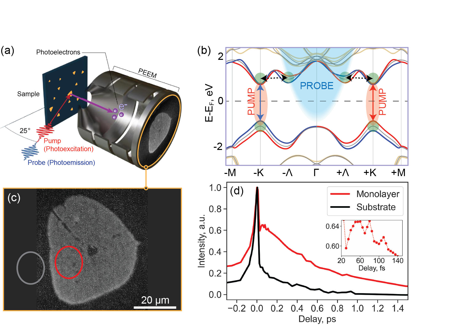
A photoemission image of a typical WS2 monolayer flake is shown in Figure 1c. Similar flakes have been characterized previously46, 47, 48 revealing the energy of main exciton resonance of 2 eV and that of charged excitons (trions) a few tens of meV (charging energy) below. In TR-PEEM experiments reported here, the energy of pump pulses was tuned to overlap the main exciton resonance thus promoting adiabatic exciton formation20, 1. The broad spectrum of the pump pulses also overlapped the energy of trions. The resulting coherent exciton polarization is expected to loose its coherence within 100 fs20, 1 giving rise to incoherent excitons and trions. Pump-induced dynamics was then monitored via probe-induced photoemission. By construction of our experiment, TR-PEEM is sensitive to dark intervalley carriers inaccessible by conventional optical spectroscopies. Measured typical pump-probe traces from substrate and interior of monolayer WS2 are shown in Figure 1d. Similar traces were also observed from other flakes on the substrate. In contrast to the substrate, monolayer WS2 features a prominent well-resolved rise of photoemission signal on a sub-100-fs time scale.
Prior to the more-detaied analysis of the observed carrier dynamics, we assess whether substrate could potentially contribute photoemission background to the measured pump-probe signals across the monolayer flake. The work function of Si and SiO2 have been previously reported to be 4.8 eV and 4.4 eV, respectively49. Given pump (2.0 eV) and probe (4.7 eV) energies used in this work, it is likely for substrate-electrons to be photoemitted from at least SiO2 layer with excess energy (electron kinetic energy) in the range of 0.3–2.3 eV. The de Broglie wavelength of such electrons is estimated as ( is electron’s mass, and is Planck’s constant) yielding the values in the range of 0.81–1.22 nm, which are larger than the thickness 0.6 nm of WS2 monolayer50. Therefore, we, generally, expect a photoemission background from the substrate to contribute to the detected transient photoemission signals obtained from monolayer region. We thus use photoemission from the substrate as an estimate for such background and subtract it from the overall photoemission signal in a manner that naturally suppresses coherent exciton contributions in pump-probe traces (see Supplementary material, Section S4, for more details). The retrieved transient WS2-specific photoemission contrast is shown in Figure 2. As expected, these differential dynamics feature delayed rise of photoemission signal followed by its subsequent decay. To gain more insights into the underlying carrier dynamics, we applied a simple fitting model to the resultant traces (see Supplementary material, Section S5), which takes into account the finite rise of the detected signal51, 20,
| (2) |
where is the time-constant describing the sub-100-fs photoemission build-up; describe subsequent dynamics beyond 100 fs; are corresponding fitting amplitudes; and are constant photoemission offset and time-zero calibration, respectively.
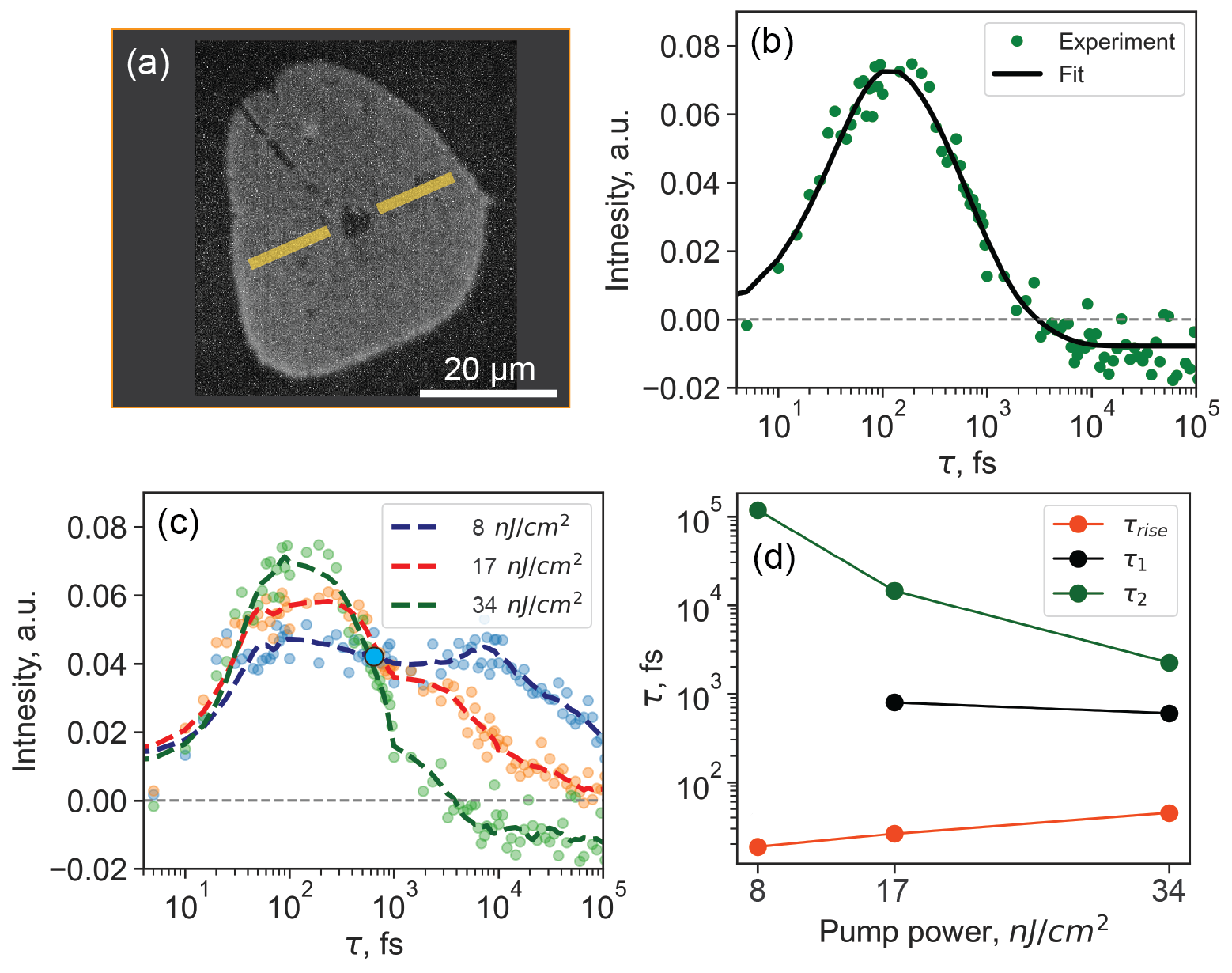
Figure 2b shows a result of fitting applied to a pump-probe trace obtained with 34 pump pulses, featuring a high fitting quality. We note a negative offset at longer delays indicating relative photoemission from the flake being less than that from the substrate, which is likely due to the effects of bandgap renormalization52, 53, 54, 55. Such renormalization could result in -valleys lowering their energy below the photoemission horizon and/or a less energetically-favourable scattering to the probe region (if K-valleys become lower in energy than -valleys). Regardless of these possible mechanisms, the net effect from both of them is the reduction in photoemission signal for higher pump fluences. Therefore, to provide a support for the hypothesis of the bandgap renormalization effects, we measured pump-induced photoemission for higher pump fluences resulting in even weaker photoemission signal (see Supplementary material, Section S6).
The retrieved time-constants are fs, ps, and ps. They are similar to those of previously-reported processes in 2D TMdC-based semiconductors, namely, (rise) exciton formation23, 20 and K-to- intervalley scattering23, 1, (1,2) reversal -to-K intervalley scattering23, exciton decay18, 34, exciton-exciton annihilation23, and formation of trions51. Due to very low excitation densities used in our experiments, we exclude exciton-exciton annihilation processes. Geminate exciton formation occurs outside the probe region and therefore should not contribute to photoemission either. In addition, it should be independent of pump fluence, but scattering processes are, in contrast, pump-fluence dependent. In the latter case, we note that for such low excitation densities used in this work, exciton-exciton scattering is not plausible intervalley transfer mechanism, and it is rather scattering mediated by phonons56, 57 and/or plasmons58 (due to intrinsic n-doping of CVD-grown monolayers59) that would be at play in this case. To confirm scattering processes taking place and to gain a further insight into the detected sub-100-fs photoemission rise and subsequent dynamics, we acquired pump-fluence dependences of pump-probe signals (Figure 2c,d).
Figure 2c shows pump-probe dynamics measured for three pump fluences of 8 , 17 , and 34 . Interestingly, fluence-dependent change of amplitudes occurs in opposite directions for delays shorter and longer than 700 fs. Specifically, for delays fs photoemission intensity overall increases with pump fluence, whereas for delays fs photoemission intensity decreases. This behaviour indicates a possible interplay of competing processes, which is also supported by the observation of a second rising signal (peaking at 7 ps) most prominent in the pump-probe dynamics obtained with the lowest pump fluence of 8 . This observation points at a possible sequential carrier-transfer phenomenon that becomes more dominant for low pump fluences. The delay of 700 fs, in this case, can be regarded as isometric point60 in the temporal domain, i.e., the point at which signal is independent of pump fluence (which is in agreement with nearly constant for higher pump fluences). We note that the chosen model (Eq. (2)) fits well the two higher-fluence pump-probe traces, but does not take explicitly into account this secondary carrier transfer observed in the low-fluence case. Instead, by applying a fitting model that takes into account two rising and decaying signals (see Supplementary material, Section S7), we can obtain a better fit to the pump-probe trace for the lowest excitation density. In this case, signal rise times of fs and ps are retrieved, which are in agreement with the reported values of intervalley exciton scattering23, 1 and trion formation51, respectively. In Figure 2c, nevertheless, the fluence-dependent trends are extracted using the model described by Eq. (2) for consistency.
All three time-constants, overall, are fluence-dependent (Figure 2d) pointing at contributions of scattering-mediated processes, with increasing, and decreasing with pump fluence; the time-constant initially increases and then decreases for increasing pump fluence (see Supplementary material, Section S5), which also supports an interplay of competing processes mentioned above. A lower scattering rate, as indicated by larger , for larger pump-fluences further points at the above-mentioned likely additional effects of bandgap renormalization. The decreasing trend for also additionally supports the above-mentioned second signal-rise wave, which in this case could reflect, indirectly, backscattering from to valleys or, directly, decay to longer-lived defect states (such as those introduced by S-vacancies) and/or generation of trions. To disentangle all these effects, further studies are required. Provided discussion above, the time-constant could reflect an interplay between exciton decay to lower states (such as traps and trions) within the probe region, and -to-K carrier scattering away from the probe region. Thus, for lower fluences, it is the exciton decay to longer-lived states that is prevalent resulting in lower rates and prominent second rise of photoemission. For higher fluences, when bandgap renormalization takes place, energetically-lowered K-valleys could result in a more efficient backscattering.
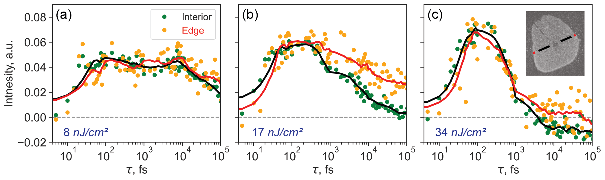
We finally note that the measured carrier dynamics is most likely defects-mediated. It has been observed previously that edges in CVD-grown WS2 monolayers contain larger amount of S-vacancies compared to the interior61, 44, 62. Defect densities in the interior can be as large as 1013 , whereas those near the edges of the order of 1014 44, which are 2–3 orders of magnitude larger than excitation densities in this work (see also Ref.61). Owing to the high spatial resolution of the method, we can, in a straightforward way, recognize contributions from defect states to the detected response by comparing pump-probe dynamics from interior (with a lesser number of S-vacancies) and edges (with a larger density of S-vacancies) of the monolayer flake. Figure 3 shows pump-probe dynamics from interior and edges for the three investigated pump fluences. In all cases, a slower decay dynamics from the edges is evident confirming contributions from trap-mediated exciton dynamics across the flake. Notably, the intervalley scattering rates are not much different between the interior and edges of monolayer flake (see Supplementary material, Section S5) indicating that defects likely do not act as efficient scattering centers in this case. Provided all the observed dynamics in this study, we conclude that dark excitons form within 14–50 fs (within the range of set experimental conditions), matching the previously reported value1.
4 Conclusion
In summary, we investigated intervalley carrier dynamics in monolayer WS2 via PEEM coupled to a femtosecond pump-probe spectroscopy with very-high temporal resolution of 13 fs. We identified initial K-to- intervalley scattering (formation of dark excitons) occurring on a time scale of 14–50 fs, depending on the excitation and defect density. The intervalley scattering does not appear to differ significantly between edges and interior of WS2 monolayer. Subsequent dynamics suggested a decay of dark excitons to longer-lived states. Defects-mediated dynamics in this case was unambiguously identified by taking advantage of imaging capabilities of the apparatus with sub-diffraction-limited spatial resolution of 75 nm. The developed spectroscopy approach can be used for identification of sub-100-fs processes in other TMdC monolayers as well as graphene63 and other topological semimetals64. Furthermore, complimenting ultrafast TR-PEEM method with excitation frequency resolution30 and energy resolution of the photoemitted electrons will provide a more comprehensive picture of the ultrafast processes taking place in these materials.
Acknowledgements
The work was supported by Vetenskapsrådet, Crafoordska Stiftelsen, and NanoLund. M.S.F. acknowledges support from the Australian Research Council (DP200101345 and CE170100039).
Authors disclosure statement
Authors declare no competing financial interests.
The following file is available as Supplementary material:
-
•
supplementary.pdf
References
- Wallauer et al. 2021 Wallauer, R.; Perea-Causin, R.; Münster, L.; Zajusch, S.; Brem, S.; Güdde, J.; Tanimura, K.; Lin, K.-Q.; Huber, R.; Malic, E.; Höfer, U. Momentum-Resolved Observation of Exciton Formation Dynamics in Monolayer WS2. Nano Letters 2021, 21, 5867–5873
- Mueller and Malic 2018 Mueller, T.; Malic, E. Exciton physics and device application of two-dimensional transition metal dichalcogenide semiconductors. npj 2D Materials and Applications 2018, 2, 29
- Chernikov et al. 2015 Chernikov, A.; Ruppert, C.; Hill, H. M.; Rigosi, A. F.; Heinz, T. F. Population inversion and giant bandgap renormalization in atomically thin WS2 layers. Nature Photonics 2015, 9, 466–470
- Splendiani et al. 2010 Splendiani, A.; Sun, L.; Zhang, Y.; Li, T.; Kim, J.; Chim, C.-Y.; Galli, G.; Wang, F. Emerging Photoluminescence in Monolayer MoS2. Nano Letters 2010, 10, 1271–1275
- Mak et al. 2012 Mak, K. F.; He, K.; Lee, C.; Lee, G. H.; Hone, J.; Heinz, T. F.; Shan, J. Tightly bound trions in monolayer MoS2. Nature Materials 2012, 12, 207–211
- You et al. 2015 You, Y.; Zhang, X.-X.; Berkelbach, T. C.; Hybertsen, M. S.; Reichman, D. R.; Heinz, T. F. Observation of biexcitons in monolayer WSe2. Nature Physics 2015, 11, 477–481
- Hao et al. 2017 Hao, K.; Specht, J. F.; Nagler, P.; Xu, L.; Tran, K.; Singh, A.; Dass, C. K.; Schüller, C.; Korn, T.; Richter, M.; Knorr, A.; Li, X.; Moody, G. Neutral and charged inter-valley biexcitons in monolayer MoSe2. Nature Communications 2017, 8, 15552
- Sie et al. 2015 Sie, E. J.; Frenzel, A. J.; Lee, Y.-H.; Kong, J.; Gedik, N. Intervalley biexcitons and many-body effects in monolayer MoS2. Physical Review B 2015, 92, 125417
- Kogar et al. 2017 Kogar, A.; Rak, M. S.; Vig, S.; Husain, A. A.; Flicker, F.; Joe, Y. I.; Venema, L.; MacDougall, G. J.; Chiang, T. C.; Fradkin, E.; van Wezel, J.; Abbamonte, P. Signatures of exciton condensation in a transition metal dichalcogenide. Science 2017, 358, 1314–1317
- Sun et al. 2021 Sun, B.; Zhao, W.; Palomaki, T.; Fei, Z.; Runburg, E.; Malinowski, P.; Huang, X.; Cenker, J.; Cui, Y.-T.; Chu, J.-H.; Xu, X.; Ataei, S. S.; Varsano, D.; Palummo, M.; Molinari, E.; Rontani, M.; Cobden, D. H. Evidence for equilibrium exciton condensation in monolayer WTe2. Nature Physics 2021, 18, 94–99
- Li et al. 2021 Li, J.; Goryca, M.; Choi, J.; Xu, X.; Crooker, S. A. Many-Body Exciton and Intervalley Correlations in Heavily Electron-Doped WSe2 Monolayers. Nano Letters 2021, 22, 426–432
- Xiao et al. 2021 Xiao, K.; Yan, T.; Liu, Q.; Yang, S.; Kan, C.; Duan, R.; Liu, Z.; Cui, X. Many-Body Effect on Optical Properties of Monolayer Molybdenum Diselenide. The Journal of Physical Chemistry Letters 2021, 12, 2555–2561
- Chernikov et al. 2014 Chernikov, A.; Berkelbach, T. C.; Hill, H. M.; Rigosi, A.; Li, Y.; Aslan, B.; Reichman, D. R.; Hybertsen, M. S.; Heinz, T. F. Exciton Binding Energy and Nonhydrogenic Rydberg Series in Monolayer WS2. Physical Review Letters 2014, 113, 076802
- Su et al. 2022 Su, H.; Xu, D.; Cheng, S.-W.; Li, B.; Liu, S.; Watanabe, K.; Taniguchi, T.; Berkelbach, T. C.; Hone, J. C.; Delor, M. Dark-Exciton Driven Energy Funneling into Dielectric Inhomogeneities in Two-Dimensional Semiconductors. Nano Letters 2022, 22, 2843–2850
- Lin et al. 2023 Lin, J.-D.; Lo, P.-Y.; Peng, G.-H.; Li, W.-H.; Huang, S.-Y.; Chen, G.-Y.; Cheng, S.-J. Essential role of momentum-forbidden dark excitons in the energy transfer responses of monolayer transition-metal dichalcogenides. npj 2D Materials and Applications 2023, 7, 51
- Chand et al. 2023 Chand, S. B.; Woods, J. M.; Quan, J.; Mejia, E.; Taniguchi, T.; Watanabe, K.; Alù, A.; Grosso, G. Interaction-driven transport of dark excitons in 2D semiconductors with phonon-mediated optical readout. Nature Communications 2023, 14, 3712
- Katzer et al. 2023 Katzer, M.; Kovalchuk, S.; Greben, K.; Bolotin, K. I.; Selig, M.; Knorr, A. Impact of dark excitons on Förster-type resonant energy transfer between dye molecules and atomically thin semiconductors. Physical Review B 2023, 107, 035304
- Ceballos et al. 2016 Ceballos, F.; Cui, Q.; Bellus, M. Z.; Zhao, H. Exciton formation in monolayer transition metal dichalcogenides. Nanoscale 2016, 8, 11681–11688
- Steinleitner et al. 2017 Steinleitner, P.; Merkl, P.; Nagler, P.; Mornhinweg, J.; Schüller, C.; Korn, T.; Chernikov, A.; Huber, R. Direct Observation of Ultrafast Exciton Formation in a Monolayer of WSe2. Nano Letters 2017, 17, 1455–1460
- Trovatello et al. 2020 Trovatello, C.; Katsch, F.; Borys, N. J.; Selig, M.; Yao, K.; Borrego-Varillas, R.; Scotognella, F.; Kriegel, I.; Yan, A.; Zettl, A.; Schuck, P. J.; Knorr, A.; Cerullo, G.; Conte, S. D. The ultrafast onset of exciton formation in 2D semiconductors. Nature Communications 2020, 11, 5277
- Li et al. 2020 Li, Y.; Liu, W.; Wang, Y.; Xue, Z.; Leng, Y.-C.; Hu, A.; Yang, H.; Tan, P.-H.; Liu, Y.; Misawa, H.; Sun, Q.; Gao, Y.; Hu, X.; Gong, Q. Ultrafast Electron Cooling and Decay in Monolayer WS2 Revealed by Time- and Energy-Resolved Photoemission Electron Microscopy. Nano Letters 2020, 20, 3747–3753
- Hein et al. 2016 Hein, P.; Stange, A.; Hanff, K.; Yang, L. X.; Rohde, G.; Rossnagel, K.; Bauer, M. Momentum-resolved hot electron dynamics at the 2-MoS2 surface. Physical Review B 2016, 94, 205406
- Wang et al. 2018 Wang, L.; Xu, C.; Li, M.-Y.; Li, L.-J.; Loh, Z.-H. Unraveling Spatially Heterogeneous Ultrafast Carrier Dynamics of Single-Layer WSe2 by Femtosecond Time-Resolved Photoemission Electron Microscopy. Nano Letters 2018, 18, 5172–5178
- Bao et al. 2020 Bao, D.; del Águila, A. G.; Thu Ha Do, T.; Liu, S.; Pei, J.; Xiong, Q. Probing momentum-indirect excitons by near-resonance photoluminescence excitation spectroscopy in WS2 monolayer. 2D Materials 2020, 7, 031002
- Sun et al. 2014 Sun, D.; Rao, Y.; Reider, G. A.; Chen, G.; You, Y.; Brézin, L.; Harutyunyan, A. R.; Heinz, T. F. Observation of Rapid Exciton–Exciton Annihilation in Monolayer Molybdenum Disulfide. Nano Letters 2014, 14, 5625–5629
- Erkensten et al. 2021 Erkensten, D.; Brem, S.; Wagner, K.; Gillen, R.; Perea-Causín, R.; Ziegler, J. D.; Taniguchi, T.; Watanabe, K.; Maultzsch, J.; Chernikov, A.; Malic, E. Dark exciton-exciton annihilation in monolayer WSe2. Physical Review B 2021, 104, l241406
- Lee et al. 2022 Lee, Y.; Tran, T. T.; Kim, Y.; Roy, S.; Taniguchi, T.; Watanabe, K.; Jang, J. I.; Kim, J. Enhanced Radiative Exciton Recombination in Monolayer WS2 on the hBN Substrate Competing with Nonradiative Exciton–Exciton Annihilation. ACS Photonics 2022, 9, 873–879
- Herman et al. 2022 Herman, A. P.; Zelewski, S. J.; Misztal, K.; Kudrawiec, R. Probing the long-lived photo-generated charge carriers in transition metal dichalcogenides by time-resolved microwave photoconductivity. Nanophotonics 2022, 11, 1335–1344
- Reding et al. 2021 Reding, J.; Zhang, W.; Allam, J. Imaging Excited-State Dynamics in Two-Dimensional Semiconductors with Emerging Ultrafast Measurement Techniques. Accounts of Materials Research 2021, 2, 75–85
- Huber et al. 2019 Huber, B.; Pres, S.; Wittmann, E.; Dietrich, L.; Lüttig, J.; Fersch, D.; Krauss, E.; Friedrich, D.; Kern, J.; Lisinetskii, V.; Hensen, M.; Hecht, B.; Bratschitsch, R.; Riedle, E.; Brixner, T. Space- and time-resolved UV-to-NIR surface spectroscopy and 2D nanoscopy at 1 MHz repetition rate. Review of Scientific Instruments 2019, 90, 113103
- Xu et al. 2020 Xu, C.; Yong, H. W.; He, J.; Long, R.; Cadore, A. R.; Paradisanos, I.; Ott, A. K.; Soavi, G.; Tongay, S.; Cerullo, G.; Ferrari, A. C.; Prezhdo, O. V.; Loh, Z.-H. Weak Distance Dependence of Hot-Electron-Transfer Rates at the Interface between Monolayer MoS2 and Gold. ACS Nano 2020, 15, 819–828
- Sass and El-Khoury 2021 Sass, P. M.; El-Khoury, P. Z. Femtosecond-Nanometer Visualization of Exciton Dynamics in MoSe2. arXiv 2021, 2109.12089
- Liang et al. 2021 Liang, Y.; Li, B.-H.; Li, Z.; Zhang, G.; Sun, J.; Zhou, C.; Tao, Y.; Ye, Y.; Ren, Z.; Yang, X. Spatially heterogeneous ultrafast interfacial carrier dynamics of 2D-MoS2 flakes. Materials Today Physics 2021, 21, 100506
- Madéo et al. 2020 Madéo, J.; Man, M. K. L.; Sahoo, C.; Campbell, M.; Pareek, V.; Wong, E. L.; Al-Mahboob, A.; Chan, N. S.; Karmakar, A.; Mariserla, B. M. K.; Li, X.; Heinz, T. F.; Cao, T.; Dani, K. M. Directly visualizing the momentum-forbidden dark excitons and their dynamics in atomically thin semiconductors. Science 2020, 370, 1199–1204
- Helmrich et al. 2021 Helmrich, S.; Sampson, K.; Huang, D.; Selig, M.; Hao, K.; Tran, K.; Achstein, A.; Young, C.; Knorr, A.; Malic, E.; Woggon, U.; Owschimikow, N.; Li, X. Phonon-Assisted Intervalley Scattering Determines Ultrafast Exciton Dynamics in MoSe2 Bilayers. Physical Review Letters 2021, 127, 157403
- Bertoni et al. 2016 Bertoni, R.; Nicholson, C.; Waldecker, L.; Hübener, H.; Monney, C.; Giovannini, U. D.; Puppin, M.; Hoesch, M.; Springate, E.; Chapman, R.; Cacho, C.; Wolf, M.; Rubio, A.; Ernstorfer, R. Generation and Evolution of Spin-, Valley-, and Layer-Polarized Excited Carriers in Inversion-Symmetric WSe2. Physical Review Letters 2016, 117, 277201
- Dong et al. 2021 Dong, S.; Puppin, M.; Pincelli, T.; Beaulieu, S.; Christiansen, D.; Hübener, H.; Nicholson, C. W.; Xian, R. P.; Dendzik, M.; Deng, Y.; Windsor, Y. W.; Selig, M.; Malic, E.; Rubio, A.; Knorr, A.; Wolf, M.; Rettig, L.; Ernstorfer, R. Direct measurement of key exciton properties: Energy, dynamics, and spatial distribution of the wave function. Natural Sciences 2021, 1, e10010
- Baum et al. 2004 Baum, P.; Lochbrunner, S.; Riedle, E. Tunable sub-10-fs ultraviolet pulses generated by achromatic frequency doubling. Optics Letters 2004, 29, 1686
- Bruder et al. 2021 Bruder, L.; Wittenbecher, L.; Kolesnichenko, P. V.; Zigmantas, D. Generation and compression of 10-fs deep ultraviolet pulses at high repetition rate using standard optics. Optics Express 2021, 29, 25593
- Zhang et al. 2018 Zhang, Q.; Lu, J.; Wang, Z.; Dai, Z.; Zhang, Y.; Huang, F.; Bao, Q.; Duan, W.; Fuhrer, M. S.; Zheng, C. Reliable Synthesis of Large-Area Monolayer WS2 Single Crystals, Films, and Heterostructures with Extraordinary Photoluminescence Induced by Water Intercalation. Advanced Optical Materials 2018, 6, 1701347
- Giannozzi et al. 2009 Giannozzi, P.; Baroni, S.; Bonini, N.; Calandra, M.; Car, R.; Cavazzoni, C.; Ceresoli, D.; Chiarotti, G. L.; Cococcioni, M.; Dabo, I.; Dal Corso, A.; de Gironcoli, S.; Fabris, S.; Fratesi, G.; Gebauer, R.; Gerstmann, U.; Gougoussis, C.; Kokalj, A.; Lazzeri, M.; Martin-Samos, L. et al. QUANTUM ESPRESSO: a modular and open-source software project for quantum simulations of materials. Journal of Physics: Condensed Matter 2009, 21, 395502
- Buckanie et al. 2009 Buckanie, N. M.; Göhre, J.; Zhou, P.; von der Linde, D.; Horn-von Hoegen, M.; Meyer zu Heringdorf, F.-J. Space charge effects in photoemission electron microscopy using amplified femtosecond laser pulses. Journal of Physics: Condensed Matter 2009, 21, 314003
- Pei et al. 2023 Pei, J.; Liu, X.; del Águila, A. G.; Bao, D.; Liu, S.; Amara, M.-R.; Zhao, W.; Zhang, F.; You, C.; Zhang, Y.; Watanabe, K.; Taniguchi, T.; Zhang, H.; Xiong, Q. Switching of K-Q intervalley trions fine structure and their dynamics in n-doped monolayer WS2. Opto-Electronic Advances 2023, 6, 220034–220034
- Carozo et al. 2017 Carozo, V.; Wang, Y.; Fujisawa, K.; Carvalho, B. R.; McCreary, A.; Feng, S.; Lin, Z.; Zhou, C.; Perea-López, N.; Elías, A. L.; Kabius, B.; Crespi, V. H.; Terrones, M. Optical identification of sulfur vacancies: Bound excitons at the edges of monolayer tungsten disulfide. Science Advances 2017, 3, e160281
- Gao et al. 2021 Gao, C.; Yang, X.; Jiang, M.; Chen, L.; Chen, Z.; Singh, C. V. Synergistic vacancy defects and mechanical strain for the modulation of the mechanical, electronic and optical properties of monolayer tungsten disulfide. Physical Chemistry Chemical Physics 2021, 23, 6298–6308
- Kolesnichenko et al. 2020 Kolesnichenko, P. V.; Zhang, Q.; Yun, T.; Zheng, C.; Fuhrer, M. S.; Davis, J. A. Disentangling the effects of doping, strain and disorder in monolayer WS2 by optical spectroscopy. 2D Materials 2020, 7, 025008
- Kolesnichenko et al. 2021 Kolesnichenko, P. V.; Zhang, Q.; Zheng, C.; Fuhrer, M. S.; Davis, J. A. Multidimensional analysis of excitonic spectra of monolayers of tungsten disulphide: toward computer-aided identification of structural and environmental perturbations of 2D materials. Machine Learning: Science and Technology 2021, 2, 025021
- McCreary et al. 2016 McCreary, K. M.; Hanbicki, A. T.; Singh, S.; Kawakami, R. K.; Jernigan, G. G.; Ishigami, M.; Ng, A.; Brintlinger, T. H.; Stroud, R. M.; Jonker, B. T. The Effect of Preparation Conditions on Raman and Photoluminescence of Monolayer WS2. Scientific Reports 2016, 6, 35154
- Lindmayer 1966 Lindmayer, J. Field effect studies of the oxidized silicon surface. Solid-State Electronics 1966, 9, 225–235
- Okada et al. 2019 Okada, M.; Okada, N.; Chang, W.-H.; Endo, T.; Ando, A.; Shimizu, T.; Kubo, T.; Miyata, Y.; Irisawa, T. Gas-Source CVD Growth of Atomic Layered WS2 from WF6 and H2S Precursors with High Grain Size Uniformity. Scientific Reports 2019, 9, 17678
- Singh et al. 2016 Singh, A.; Moody, G.; Tran, K.; Scott, M. E.; Overbeck, V.; Berghäuser, G.; Schaibley, J.; Seifert, E. J.; Pleskot, D.; Gabor, N. M.; Yan, J.; Mandrus, D. G.; Richter, M.; Malic, E.; Xu, X.; Li, X. Trion formation dynamics in monolayer transition metal dichalcogenides. Physical Review B 2016, 93, 041401(R)
- Wang et al. 2013 Wang, Q.; Ge, S.; Li, X.; Qiu, J.; Ji, Y.; Feng, J.; Sun, D. Valley Carrier Dynamics in Monolayer Molybdenum Disulfide from Helicity-Resolved Ultrafast Pump–Probe Spectroscopy. ACS Nano 2013, 7, 11087–11093
- Pogna et al. 2016 Pogna, E. A. A.; Marsili, M.; De Fazio, D.; Dal Conte, S.; Manzoni, C.; Sangalli, D.; Yoon, D.; Lombardo, A.; Ferrari, A. C.; Marini, A.; Cerullo, G.; Prezzi, D. Photo-Induced Bandgap Renormalization Governs the Ultrafast Response of Single-Layer MoS2. ACS Nano 2016, 10, 1182–1188
- Cunningham et al. 2017 Cunningham, P. D.; Hanbicki, A. T.; McCreary, K. M.; Jonker, B. T. Photoinduced Bandgap Renormalization and Exciton Binding Energy Reduction in WS2. ACS Nano 2017, 11, 12601–12608
- Lin et al. 2019 Lin, T. N.; Santiago, S. R. M.; Caigas, S. P.; Yuan, C. T.; Lin, T. Y.; Shen, J. L.; Chen, Y. F. Many-body effects in doped WS2 monolayer quantum disks at room temperature. npj 2D Materials and Applications 2019, 3, 46
- Christiansen et al. 2017 Christiansen, D.; Selig, M.; Berghäuser, G.; Schmidt, R.; Niehues, I.; Schneider, R.; Arora, A.; de Vasconcellos, S. M.; Bratschitsch, R.; Malic, E.; Knorr, A. Phonon Sidebands in Monolayer Transition Metal Dichalcogenides. Physical Review Letters 2017, 119, 187402
- Raja et al. 2018 Raja, A.; Selig, M.; Berghäuser, G.; Yu, J.; Hill, H. M.; Rigosi, A. F.; Brus, L. E.; Knorr, A.; Heinz, T. F.; Malic, E.; Chernikov, A. Enhancement of Exciton–Phonon Scattering from Monolayer to Bilayer WS2. Nano Letters 2018, 18, 6135–6143
- Van Tuan et al. 2017 Van Tuan, D.; Scharf, B.; Žutić, I.; Dery, H. Marrying Excitons and Plasmons in Monolayer Transition-Metal Dichalcogenides. Physical Review X 2017, 7, 041040
- Chae et al. 2017 Chae, W. H.; Cain, J. D.; Hanson, E. D.; Murthy, A. A.; Dravid, V. P. Substrate-induced strain and charge doping in CVD-grown monolayer MoS2. Applied Physics Letters 2017, 111, 143106
- Kaspar 2023 Kaspar, F. Quality Data from Messy Spectra: How Isometric Points Increase Information Content in Highly Overlapping Spectra. ChemBioChem 2023, 24, e2022007
- Bao et al. 2015 Bao, W.; Borys, N. J.; Ko, C.; Suh, J.; Fan, W.; Thron, A.; Zhang, Y.; Buyanin, A.; Zhang, J.; Cabrini, S.; Ashby, P. D.; Weber-Bargioni, A.; Tongay, S.; Aloni, S.; Ogletree, D. F.; Wu, J.; Salmeron, M. B.; Schuck, P. J. Visualizing nanoscale excitonic relaxation properties of disordered edges and grain boundaries in monolayer molybdenum disulfide. Nature Communications 2015, 6, 7993
- Rosenberger et al. 2018 Rosenberger, M. R.; Chuang, H.-J.; McCreary, K. M.; Li, C. H.; Jonker, B. T. Electrical Characterization of Discrete Defects and Impact of Defect Density on Photoluminescence in Monolayer WS2. ACS Nano 2018, 12, 1793–1800
- Trepalin et al. 2019 Trepalin, V.; Asselberghs, I.; Brems, S.; Huyghebaert, C.; Radu, I.; Afanas’ev, V.; Houssa, M.; Stesmans, A. Evaluation of the effective work-function of monolayer graphene on silicon dioxide by internal photoemission spectroscopy. Thin Solid Films 2019, 674, 39–43
- Biswal et al. 2022 Biswal, B.; Mishra, S. B.; Yadav, R.; Poudyal, S.; Rajarapu, R.; Barman, P. K.; Pandurang, K. R.; Mandal, M.; Singh, R. P.; Nanda, B. R. K.; Misra, A. Work function of van der Waals topological semimetals: Experiment and theory. Applied Physics Letters 2022, 120, 093101
See pages - of supplementary.pdf