Observation of room temperature gate tunable quantum confinement effect in photodoped junctionless MOSFET
Abstract
In the pursuit of room temperature quantum hardware, our study introduces a gate voltage tunable quantum wire within a tri-gated n-type junctionless MOSFET. The application of gate voltage alters the parabolic potential well of the tri-gated junctionless MOSFET, enabling modification of the nanowire’s potential well profile. In the presence of light, photogenerated electrons accumulate at the center of the junctionless nanowire, aligning with the modified potential well profile influenced by gate bias. These carriers at the center are far from interfaces and experience less interfacial noise. Therefore, such clean photo-doping shows clear, repeatable peaks in current for specific gate biases compared to the dark condition, considering different operating drain-to-source voltages at room temperature. We propose that photodoping-induced subband occupation of gate tunable potential well of the nanowire is the underlying phenomenon responsible for this kind of observation. This study reveals experimental findings demonstrating gate-induced switching from semi-classical to the quantum domain, followed by the optical occupancy of electronic sub-bands at room temperature. We developed a compact model based on the Nonequilibrium Green’s function formalism to understand this phenomenon in our illuminated device better. This work reveals the survival of the quantum confinement effect at room temperature in such semi-classical transport.
I Introduction
The quantum confinement effect (QCE) is an extraordinary phenomenon in solid-state devices at cryogenic temperatures Elzerman et al. (2004); Xia and Cheah (1997); Petta et al. (2005); Angus et al. (2007); Rustagi et al. (2007); Li et al. (2013). QCE manifests when the device dimensions are on the same order of magnitude as the De Broglie wavelength of the carriers (electrons or holes), resulting in the quantization of energy levels. At ultra-low temperatures, the energy gaps between these discrete levels are significantly more significant than thermal fluctuations, enabling the distinct identification of these quantized energy levels in experiments.However, at room temperature (RT), the thermal energy vastly exceeds the energy differences between these quantized energy levels, making it highly challenging to observe QCE. Nevertheless, achieving QCE at RT is crucial for advancing quantum electronics hardware. To accomplish this, devices must be extremely thin. Fabricating such nanodevices with traditional junctions is a complex process, requiring precise doping profiles at sub-nanometer junction regions. In this context, junction-less transistors Colinge et al. (2011); Lee et al. (2009); Amin and Sarin (2013); Colinge et al. (2006a); Das et al. (2016) have gained significant attention due to their practical advantages.In the past few years, Silicon quantum dot (QD) with nanometer islands Gorman et al. (2005); Yang et al. (2016) and junctionless nanowire (Si NW) Nishiguchi et al. (2006); Shi et al. (2013); Shaji et al. (2008); MacQuarrie et al. (2020); Schoenfield et al. (2017); Penthorn et al. (2019); Hu et al. (2007) based QDs show massive potential for applications in quantum computation Elzerman et al. (2004); Petta et al. (2005); Veldhorst et al. (2015), quantum sensing Degen et al. (2017); Elzerman et al. (2004); Gonzalez-Zalba et al. (2016); Berman et al. (1997); Zhang et al. (2005), and provide a platform for CMOS-compatible nanoelectronics Nikonov and Young (2013).QCE at RT in 5 nm P-silicon [110] NW on Silicon-on-insulator (SOI) substrates by top-down approach is demonstrated experimentally Trivedi et al. (2011); Yi et al. (2011). Buin et al. (2008); Singh et al. (2008) showed enhanced performance based on RT QCE-based Si NW on SOI. SOI-based n-Si(110) NW field-effect transistor (FET) shows RT QCE, and SOI-based n-Si(100) NW FET shows RT single electron/hole transport Suzuki et al. (2013). When incident light interacts with the phototransistor, photogenerated electrons and holes disperse into the channel region by the band profile, thus modifying the carrier distribution. This, in turn, leads to a modulation in conductivity, a phenomenon known as photogating Konstantatos et al. (2012); Jiang et al. (2022); Yuan et al. (2018); Huang et al. (2016); Guo et al. (2016).For Si NW-based transistors, the interface provides a self-assembled electric field due to band bending at the interface, and this field accumulates photogenerated charges depending on the band bending; these are called photoinduced trap charges. These trap charges act as a photogate voltage, altering the carrier profile and, ultimately, the channel’s conductance. Introducing carriers into the channel region via a photogate voltage termed photo doping of the channel. Photoinduced doping is an enhanced form of doping in materials such as semiconductors under the influence of light Aftab et al. (2022); Wu et al. (2017); Yan et al. (2009); Calarco et al. (2005). Photo-generation and efficient separation of charge carriers under the influence of an inner electric field in heterojunctions have produced a photon-modulated convertibility between negative differential resistance and resistive switching in such systems Zheng et al. (2019).
II Results
In this study, we investigate the behavior of room-temperature Quantum Confinement Effect (QCE)-based transport in the presence of light. As illustrated in Figure 1a, we present a schematic representation of the tri-gated junctionless transistor we fabricated. The dimensions of the silicon nanowire (NW) are (), and the gate length is . In contrast, Figure 1b displays a scanning electron microscopic (SEM) image of the actual device, and Figure 1c is a cross-sectional tunneling electron microscope (TEM) image of the device.
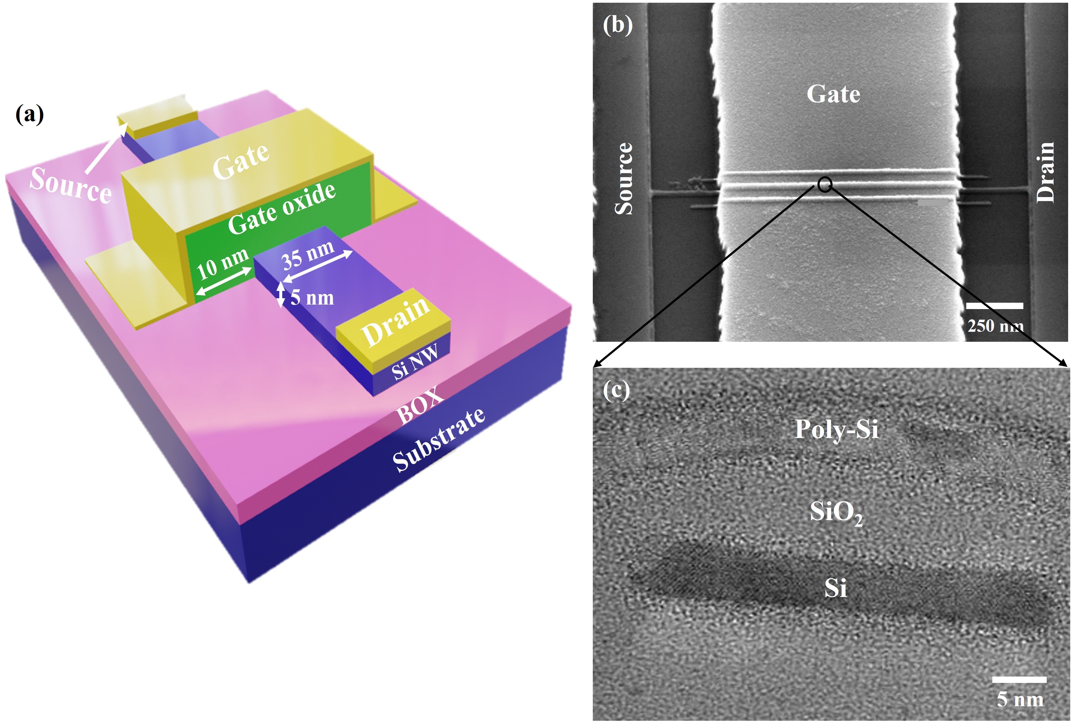
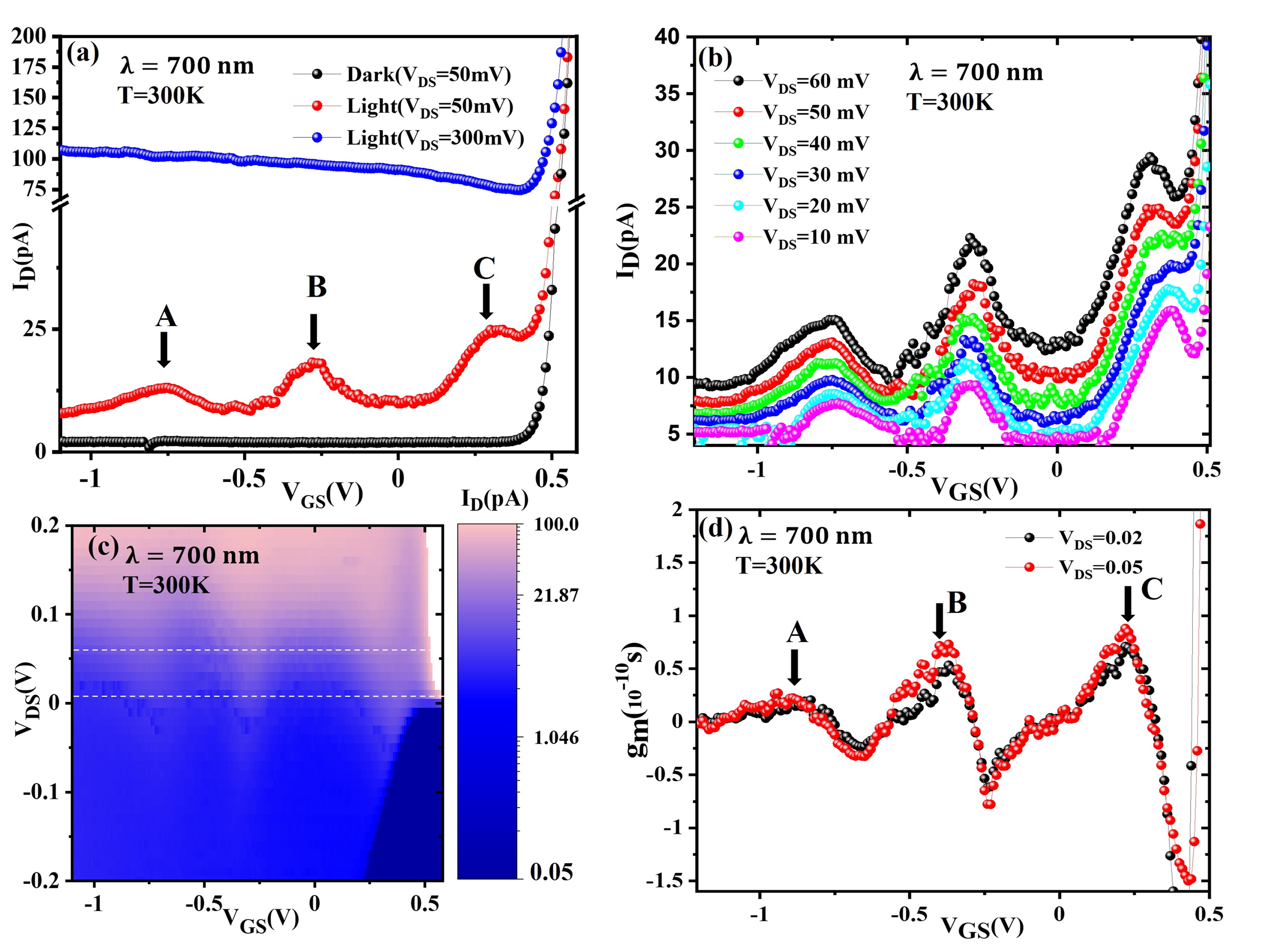
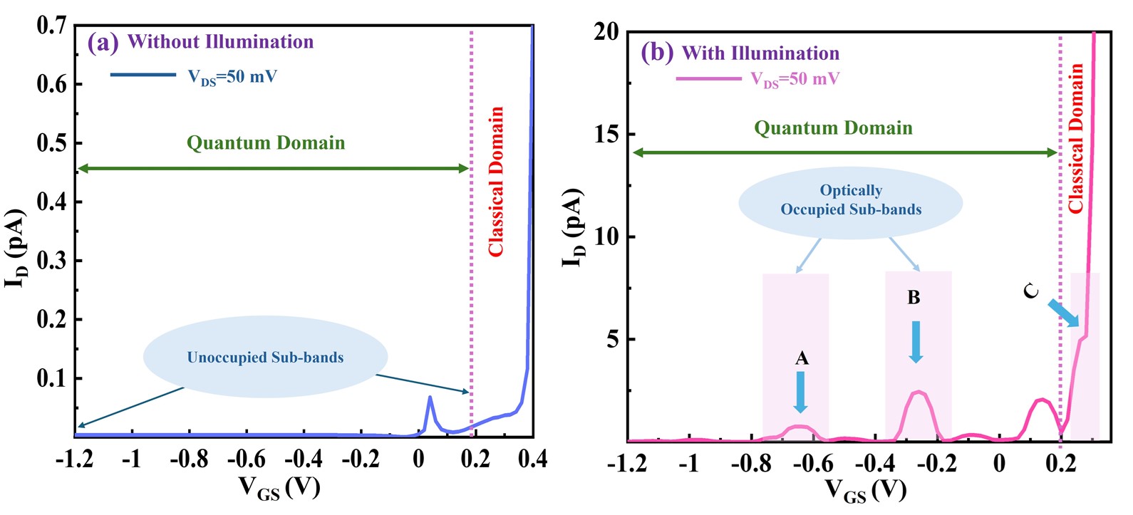
Figure 2 presents the results of photocurrent measurements for our junctionless transistor under different drain biases, specifically, at 50 mV and 300 mV when exposed to 700 nm light at room temperature (RT). Notably, a significant increase in current is observed under illumination compared to the dark current. Of particular interest is the presence of oscillations in the drain current concerning variations in gate voltage under illumination. To further investigate the influence of gate voltage on the drain current over a range of drain biases, we systematically varied the drain bias from -200 mV to 200 mV and recorded the transfer characteristics. This comprehensive examination is illustrated in the plane of drain and gate biases, as shown in Figure 2c. The graph’s white lines delineate the drain bias values range where we observed significant gate tunability. Figure 2b reveals substantial gate tunability in the photocurrent from to at RT. For higher drain bias, this tunability vanished Colinge et al. (2006a); Colinge (2007); Colinge et al. (2006b); Rustagi et al. (2007); Lee et al. (2010); Trivedi et al. (2011); Ma et al. (2015); Li et al. (2013); Je et al. (2000), which is further discussed in Section B of Supplementary Note (SN)-4 in Supplementary Information (SI) NAT (2024). To see those peaks more prominently, we plotted the transconductance with respect to gate voltage for drain voltage 20 mV and 50 mV, respectively, in Figure 2d. Transconductance behavior for other drain voltages is illustrated in Section A of SN-4 in SI NAT (2024). In addition to that, channel conductance behavior with respect to gate voltage is also illustrated in Section B of SN-4 in SI NAT (2024).
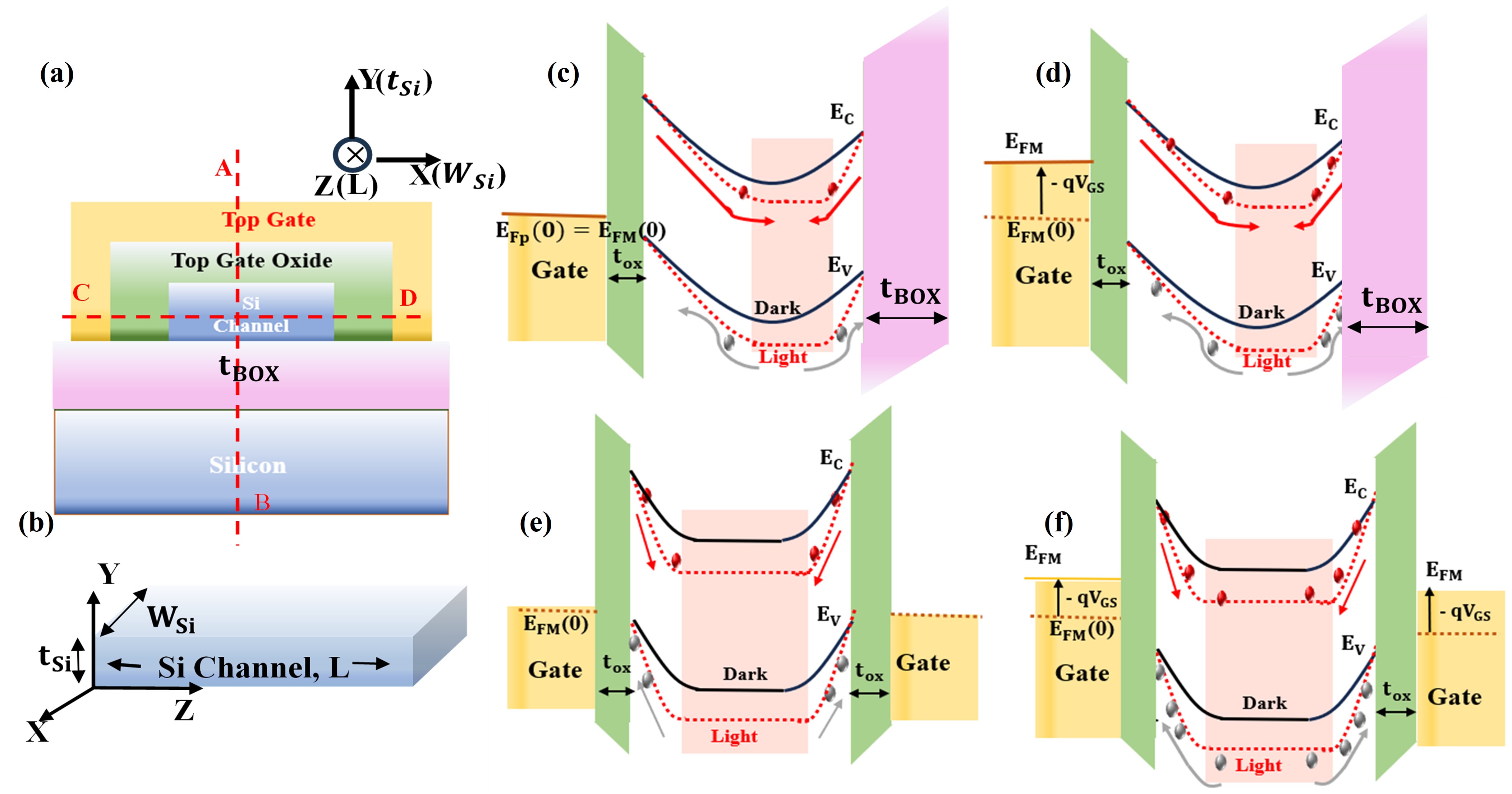
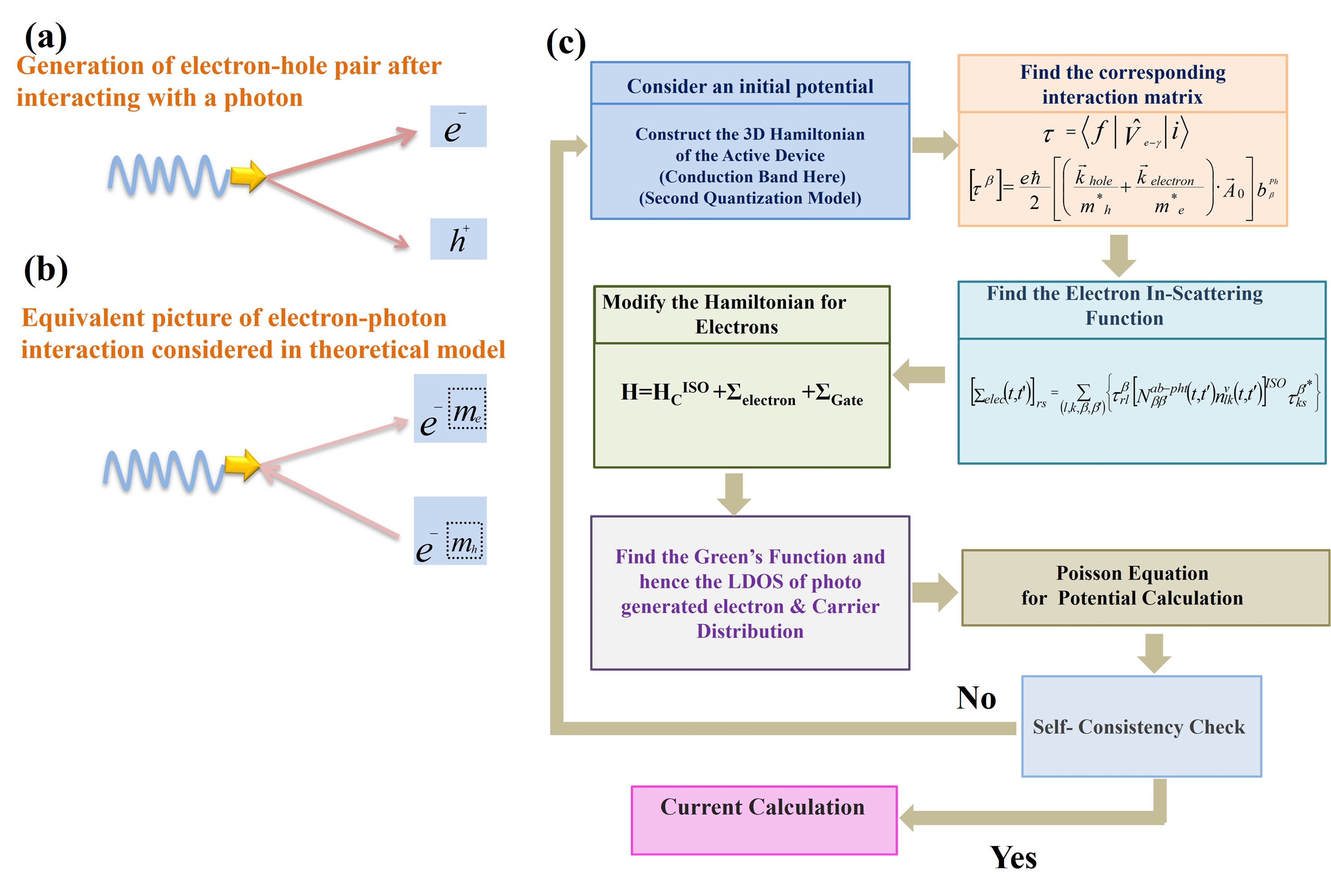
In the presence of light, an electron-hole pair (e-h pair) will be generated, and the electrons will be accumulated in the core of the channel due to band confinement, which is shown pictorially in figure-3c to 3f. To understand this electron accumulation at the center of NW more clearly, we illustrated the energy band diagrams along the cutline, denoted as the red dotted lines, namely AB and CD, respectively, in figure-3a. As the photo-generated hole moves toward the surface due to upward band bending (negative surface potential), consequently, the photo-generated electrons move toward the core of the nanowire (figure-3c to 3f). Due to this spatial quarantine of photo-generated e-h pairs, an additional positive gate voltage is induced by accumulated holes at the interface of of the NW channel, which in turn modulates the concentration of electrons at the core of n channel NW. In other words, in addition to the applied gate voltage, this also modulates the channel’s conductance. Electrons are doping the core of the nanowire (NW) due to light and potential well modification of NW due to gate bias, and we term this phenomenon the photo doping of electrons in the NW core. Upon the application of a negative gate voltage to the top gate, there will be more accumulation of holes at the interface of the (figure-3d and 3f). This can be understood in this way: when the negative gate voltage is applied to the top gate, the slope of the energy band near the interface will be stiffened compared to the no gate voltage case (figure-3c and 3e) to support the high electric field. Due to this, the availability of states near the interface will increase. Therefore, for a high electric field, more photo-generated holes will be translated toward the interface and facilitated into the increased states at the interface. Consequently, more electrons will be accumulated at the center of the channel due to the increase in efficiency in e-h pair separation and the rise in positive photo gate voltage. This electron accumulation at the center of NW is illustrated by the light shadow of pink color in figure-3d and 3f. Therefore, negative gate voltage increases the holes at the interface, and as a consequence of the increase in induced positive photo gate voltage, the concentration of electrons at the center eventually increases. In other words, band bending near the interface will increase as we increase the negative gate voltage, introducing a high recombination barrier for photo-generated e-h pairs. Our NEGF modeling effectively captures this event, as illustrated in figure-S3 of SI NAT (2024). Therefore, the efficiency of separating the photo-generated e-h pair will increase, and eventually, the concentration of electrons at the center will increase, too. We are calling it enhanced photo doping of the channel.
III Discussion
A channel of photo-generated electrons is induced at the center of the nanowire due to photo-doping effects resulting from modification of the potential well of NW due to gate voltage. This occurs through the bulk conduction mechanism of the junctionless transistor(JLT) Colinge et al. (2011, 2010); Trevisoli et al. (2012); Rai et al. (2022); Colinge (1990, 2012); Gnani et al. (2011), which is explained in SN-2 section of SI NAT (2024). To extensively clarify the photo doping in our device, we modeled device behavior using the Nonequilibrium Green’s Function Method (NEGF). The modeling starts with constructing a closed system Hamiltonian, and then we build the electron-photon interaction term, namely, the electron in scattering function. This function accounts for the excess electrons entering the system due to electron-photon interaction. Ultimately, we add this to the closed system Hamiltonian to make it an open system. After that, we perform Schrödinger-Poison’s self-consistency to find the modified Hamiltonian and consequently system Green’s function, local density of state (LDOS) in dark and illumination conditions, and carrier distribution. The motion of charges in the quantum system is described by the Schrödinger-Poisson equations in the following manner:
| (1) | ||||
| (2) |
| (3) |
where in Cartesian coordinates. depicts the charge polarity of the hole and electron, respectively. The complete Hamiltonian for this system can be expressed in the following manner :
| (4) |
where represent . is the distribution of potential energy of the conduction/valance band in and directions. and are the permittivity tensor and effective mass tensor, respectively, whose components vary at interfaces (e.g., semiconductor-insulator and metal-insulator). Pursuing the Heisenberg equation of motion, equation-4 results in the pertinent equations governing the motion of photo-generated electrons, incident photons, and holes:
| (5) |
Here, , , and denote electron annihilation operators corresponding to the state of the conduction band, state of the valence band of the fin body, and state of the reservoirs (gate), respectively. Additionally, is the annihilation operator for photons at the mode. The term represents the interaction between reservoirs and the active device (conduction band). It is worth noting that the operator’s b’s, c’s, and v’s adhere to the Bose-Einstein (BE) commutation and Fermi-Dirac (FD) anti-commutation relations, . The Keldysh formalism is now employed to evaluate the two-time correlation functions Keldysh et al. (1965).
| (6) | ||||||
, , and denote two-time correlation functions corresponding to the occupied state of electrons in the conduction band and valence band, as well as the absorbed photon, respectively. The electron and hole-in-scattering functions can be written as belowAeberhard and Morf (2008); Mera et al. (2016); Aeberhard (2012); Bertazzi et al. (2020); Kolek (2019); Sikdar et al. (2021, 2017)and which is derived in theoretical modeling section.
| (7) |
After the addition of reservoirs and in scattering function for electrons and holes, the modified green’s function can be written asDatta (2000, 2005)
| (8) |
Hence, the concentration of photo-generated electron and hole concentration per second is calculated as followsSikdar et al. (2021)
| (9) |
The transverse electronic state, n(x,y) can be split up into two transverse subspace as followsSikdar et al. (2019)
| (10) |
The 2D carrier distribution in the fin body cross-section (i.e., x-y plane) is given by,
| (11) |
Then the charge concentration at the source side and it was calculated followed by equation-11 and incorporated into equation-2 to obtain the electrostatic potential and then compared with the previous potential in the iteration loop to find the non-trivial difference self consistently(as shown in figure-6 of manuscript). Therefore, the charge concentration at the drain side for long-channel devices can be calculated by Trevisoli et al. (2012)
| (12) |
where .Therefore the surface potential-based drain current analytical expression is given byTrevisoli et al. (2012),
| (13) |
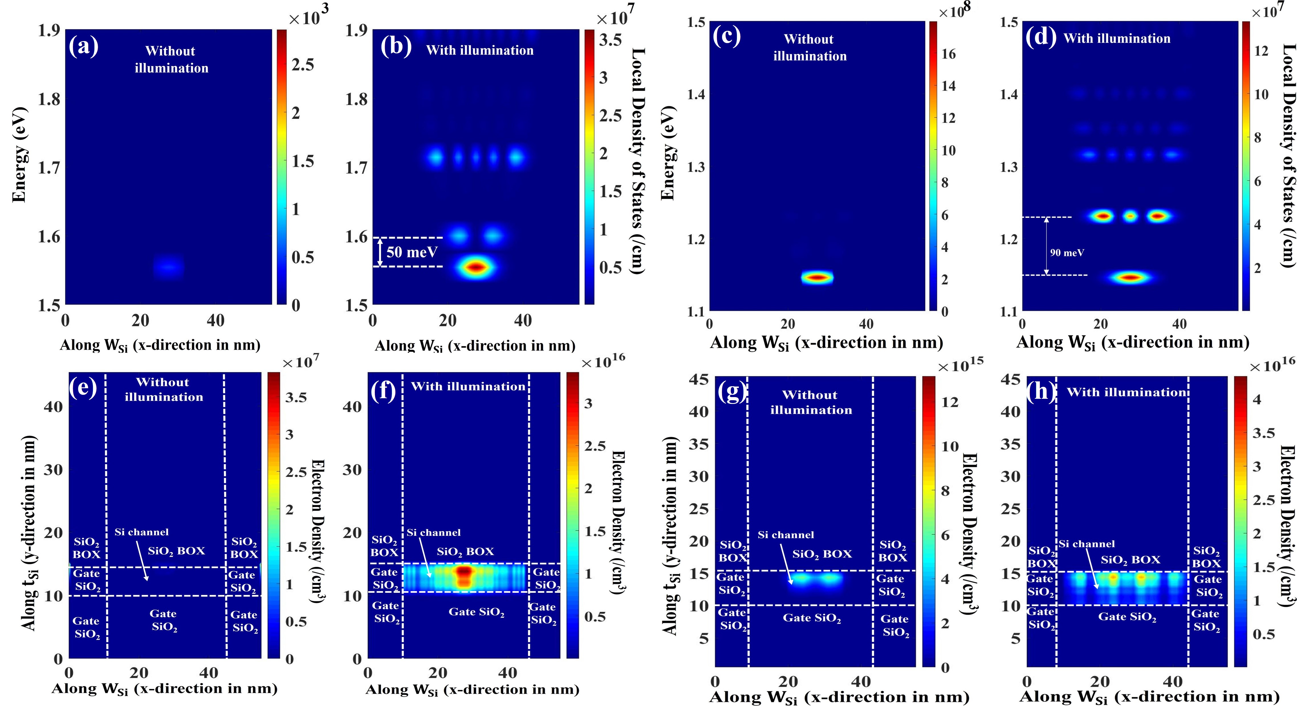
Using equation-12 and 13, we have calculated and plotted it against the gate voltage for =50 mV for non illuminated case (figure-5a) and illuminated case (figure-5b) respectively. From those two figures, we can see that for dark is almost flat due to the deficiency of electrons and the unavailability of states. This is illustrated in figure-4a and 4e for peak A, corresponding to the =-0.64V. It is also further illustrated for =-0.26V corresponding to peaks B, in figure-4c and figure-4g, respectively. In section SN-5 of SI NAT (2024) corresponding to peaks C is demonstrated. from our theoretical calculations for illuminated case shows nearly exact peaks, namely A, B, and C, respectively, for =50 mV (Figure-5b). These peaks approximately match our experimental results (figure-2a). Here, the Gate voltage is pushing the device to the quantum regime along direction, and being already in the quantum domain in direction, we finally reach voltage tunable quantum wire. A coupled mode LDOS of that quantum wire from our NEGF model is illustrated in figure-4a and figure-4b for the non-illuminated and illuminated case respectively for gate Voltage =-0.64V. This illustration demonstrates the energy difference between the initial and subsequent sub-bands is 50 meV for gate Voltage =-0.64V. Similarly, the energy spacing of the first and third sub-band is 90 meV for gate Voltage =-0.26V, which is shown in figure-4c and figure-4d respectively. The energy spacing of the first and third sub-band is 90 meV for gate Voltage =0.28V, which is illustrated in SN-5 of SI NAT (2024). These peaks A, B, and C are related optically populated subbands for different gate voltage =-0.64V,-0.26V, and 0.28V, respectively, at room temperature. Theoretically, to see clear oscillation of current due to subband population at room temperature, the subband energy separation must be equal to at least 3.5 times of thermal broadening energy () Beenakker (1991); Heinzel (2008); Yi et al. (2011), which is 91 meV. From our experiment and theoretical model, the energy spacing of the first and second subband is approximately 1.96 (for 50 meV subband spacing for =-0.64V) times of thermal broadening energy for peak A. For peaks B and C, the energy spacing of the first and third subbands is approximately 3.5 times the thermal broadening energy. Therefore, the creation of such sub-bands at room temperature and corresponding distinct optical populations due to gate tunable quantum well is justified as far as our device and its environment are concerned.
IV Conclusion
In summary, we conducted an experimental study on gate-tunable semi-classical transport in a silicon nanowire top-gated junctionless n-channel MOSFET, focusing on the quantum confinement effect when exposed to light at room temperature. We verified this gate tunability of semi-classical transport by measuring drain current while sweeping the gate voltage at various drain-to-source bias settings. Notably, this gate tunability of QCE and corresponding quantum mechanically controlled diffusive transport persisted under slight drain-to-source bias but became less discernible at higher drain-to-source bias levels. Additionally, we developed a compact model for light-electron interactions within our nanostructure device and its corresponding transport characteristics. This model helped us gain insights into the origins of the observed anomalies in transport behavior at room temperature, utilizing the nonequilibrium Green’s function (NEGF) approach. Therefore, this letter unveils an abnormality in quantum mechanically controlled diffusive transport that persists even at room temperature under the influence of illumination. This will open up new possibilities for quantum devices at room temperature by photo-doping in low-dimensional field-effect transistors.
V Methods
Theoretical Modeling: To understand the light-matter interaction, we need to find the corresponding interaction matrix, which has been conceptualized as a scattering picture as follows
| (14) |
The state preceding the scattering event depicts the virtual electron possessing the effective mass of the hole and momentum that is equal but opposite., i.e., and the final state (post-scattering) of the real electron, as shown by Feynman diagram in figure-6a.
The carrier-photon interaction operator is: =
Here, is the momentum operator, and is the incident photons’ vector potential.
Thus, the light-matter interaction matrix can be written as Aeberhard (2012); Bertazzi et al. (2020); Kolek (2019).
| (15) |
Where and
The last term of equation-17 is calculated by starting from,
Equation-19 can be solved by calculating the electron-photon Green’s function as follows.
| (20) |
Similarly can be written as,
| (21) |
substituting the equation-20 and 21 in the equation-5, we get,
| (22) |
where
| (23) |
In our device, the possibility of carrier recombination is negligible due to voltage-dependent separation. Hence, the second term of the R.H.S of equation-23 can be neglected. So, we find,
| (24) |
These entire calculations can be similarly followed for holes, and so reach to,
| (25) |
Where the number of absorbed photons is given as:
, , , and are the intensity of the laser source, correlation function of the filled states in the conduction band, valence band, and the absorbing volume, respectively. At the same time, represents the interaction potential governing the device’s photo generation (electron-hole pair). The velocity of light within the material is , where is the refractive index of Si for the corresponding wavelength of the laser source.
Device Fabrication : Figure-1a shows the schematic of a tri-gated nanowire junctionless transistor. The nanowire is highly doped () such that we can have a high amount of ON current. The gate material surrounded the nanowire from three directions, as shown in figure-1, to increase the gate control over the channel, and this tri-gate has the same functionality as a conventional single gate. Therefore, this tri-gate geometry can easily control the flow of carriers from source to drain with the highest precision. We use -type nanowire or channel and p-type gate in this work. Therefore, we now put a -type gate on the -type channel; due to work function difference and very low nanowire thickness (5 nm), the channel beneath the gate got depleted completely. So, this type of junction-less device works in accumulation mode, which is unlikely like other devices with junctions. To fabricate tri-gated silicon nanowire-based junctionless MOSFET, we used silicon-on-insulator (SOI) wafers with a few high-quality nanometers of top silicon. We did ion implantation of arsenic to dope the top silicon of SOI wafer into n-type silicon, and resultant arsenic doping was in the order of . After making the top silicon into n-type, we did nanolithography using electron beam lithography (EBL) to define the nanowire, where we spin-coated top silicon with negative electron resist Hydrogen Silsesquioxane (HSQ). Next, we did reactive ion etching (RIE) of EBL patterned nanowire, and finally, silicon nanowire (Si NW) was realized. After realizing the nanowire, we did dry oxidation of Sio2 on the top of the nanowire to get 10 nm top gate oxide. Then, we patterned the oxide over the nanowire. In the next step to realizing 1 um top gate, we deposited 50 nm amorphous silicon in a low-pressure chemical vapor chamber at . We doped the amorphous silicon heavily with boron to make top gate. After this, we annealed the sample for 30 mins at in nitrogen to make it polycrystalline silicon from amorphous silicon. Then, we did EBL and RIE to pattern the polysilicon to define the 1-um gate. To isolate the gate from source and drain contact, we deposited a very slim layer of sio2. To make source and drain contact, we opened a window in the sio2 via photolithography and deposited Ti/W-Al. The scanning electron microscopy (SEM) image of fabricated tri-gated silicon nanowire MOSFET is shown in figure-1b.The whole fabrication steps are illustrated in SN-5 of SI NAT (2024).
Photo Response Measurement: The photo responsiveness of the Tri-Gated Junctionless (JL) nanowire n-channel transistor we fabricated was assessed under light exposure with a wavelength of 700 nm. Illuminating our Nanowire MOSFET with a laser beam with incident power on the nanowire is 4.12 nW. This illumination induces electron excitation, resulting in the production of a measurable current. Subsequently, the source measuring unit captures and examines this current, offering valuable information about NW MOSFET’s photoconductivity and electronic characteristics. In Figure 2, the transfer characteristics of our fabricated device are depicted under constant illumination conditions while maintaining a fixed drain-to-source voltage of 50 mV. Even at incident power on the nanowire is 4.12 nW, our device exhibited a discernible photo response compared to the non-illuminated case, highlighting its high sensitivity. To further understand the photo response, we varied the drain-to-source voltage from -200 mV to +200 mV, maintaining the same illumination conditions ( laser beam with incident power on the nanowire is 4.12 nW and a wavelength of 700 nm).
VI Data Avaibility
The datasets produced in this research can be acquired by making a reasonable request to the corresponding author.
VII Acknowledgement
The authors thank the Defence Research and Development Organisation (DRDO) and the Department of Science and Technology (DST) for financial support. BK acknowledges the financial assistance from the Prime Minister Research Fellows (PMRF) Scheme (PMRF ID: 1401633), India. Additionally, special appreciation is expressed to James Haigh from Hitachi Cambridge Laboratory for assisting with optical measurements.
VIII Author Contributions
BK and AM have made equal contributions to this article.
IX Competing interests
The authors declare no competing interests.
Correspondence and inquiries for materials should be directed to S.D.
References
- Elzerman et al. (2004) J. Elzerman, R. Hanson, L. Willems van Beveren, B. Witkamp, L. Vandersypen, and L. P. Kouwenhoven, nature 430, 431 (2004).
- Xia and Cheah (1997) J.-B. Xia and K. Cheah, Physical Review B 55, 15688 (1997).
- Petta et al. (2005) J. R. Petta, A. C. Johnson, J. M. Taylor, E. A. Laird, A. Yacoby, M. D. Lukin, C. M. Marcus, M. P. Hanson, and A. C. Gossard, Science 309, 2180 (2005).
- Angus et al. (2007) S. J. Angus, A. J. Ferguson, A. S. Dzurak, and R. G. Clark, Nano letters 7, 2051 (2007).
- Rustagi et al. (2007) S. C. Rustagi, N. Singh, Y. Lim, G. Zhang, S. Wang, G. Lo, N. Balasubramanian, and D.-L. Kwong, IEEE electron device letters 28, 909 (2007).
- Li et al. (2013) X. Li, W. Han, L. Ma, H. Wang, Y. Zhang, and F. Yang, IEEE electron device letters 34, 581 (2013).
- Colinge et al. (2011) J.-P. Colinge, C.-W. Lee, N. Dehdashti Akhavan, R. Yan, I. Ferain, P. Razavi, A. Kranti, and R. Yu, Semiconductor-On-Insulator Materials for Nanoelectronics Applications pp. 187–200 (2011).
- Lee et al. (2009) C.-W. Lee, A. Afzalian, N. D. Akhavan, R. Yan, I. Ferain, and J.-P. Colinge, Applied Physics Letters 94 (2009).
- Amin and Sarin (2013) S. I. Amin and R. Sarin, in Third International Conference on Computational Intelligence and Information Technology (CIIT 2013) (IET, 2013), pp. 432–439.
- Colinge et al. (2006a) J.-P. Colinge, A. J. Quinn, L. Floyd, G. Redmond, J. C. Alderman, W. Xiong, C. R. Cleavelin, T. Schulz, K. Schruefer, G. Knoblinger, et al., IEEE Electron Device Letters 27, 120 (2006a).
- Das et al. (2016) S. Das, V. Dhyani, Y. M. Georgiev, and D. A. Williams, Applied Physics Letters 108 (2016).
- Gorman et al. (2005) J. Gorman, D. Hasko, and D. Williams, Physical review letters 95, 090502 (2005).
- Yang et al. (2016) T.-Y. Yang, A. Andreev, Y. Yamaoka, T. Ferrus, S. Oda, T. Kodera, and D. A. Williams, in 2016 IEEE International Electron Devices Meeting (IEDM) (IEEE, 2016), pp. 34–2.
- Nishiguchi et al. (2006) K. Nishiguchi, A. Fujiwara, Y. Ono, H. Inokawa, and Y. Takahashi, Applied physics letters 88 (2006).
- Shi et al. (2013) Z. Shi, C. Simmons, D. R. Ward, J. Prance, R. Mohr, T. S. Koh, J. K. Gamble, X. Wu, D. Savage, M. Lagally, et al., Physical Review B 88, 075416 (2013).
- Shaji et al. (2008) N. Shaji, C. Simmons, M. Thalakulam, L. J. Klein, H. Qin, H. Luo, D. Savage, M. Lagally, A. Rimberg, R. Joynt, et al., Nature Physics 4, 540 (2008).
- MacQuarrie et al. (2020) E. MacQuarrie, S. F. Neyens, J. Dodson, J. Corrigan, B. Thorgrimsson, N. Holman, M. Palma, L. Edge, M. Friesen, S. Coppersmith, et al., npj Quantum Information 6, 81 (2020).
- Schoenfield et al. (2017) J. S. Schoenfield, B. M. Freeman, and H. Jiang, Nature communications 8, 64 (2017).
- Penthorn et al. (2019) N. E. Penthorn, J. S. Schoenfield, J. D. Rooney, L. F. Edge, and H. Jiang, npj Quantum Information 5, 94 (2019).
- Hu et al. (2007) Y. Hu, H. O. Churchill, D. J. Reilly, J. Xiang, C. M. Lieber, and C. M. Marcus, Nature nanotechnology 2, 622 (2007).
- Veldhorst et al. (2015) M. Veldhorst, C. Yang, J. Hwang, W. Huang, J. Dehollain, J. Muhonen, S. Simmons, A. Laucht, F. Hudson, K. M. Itoh, et al., Nature 526, 410 (2015).
- Degen et al. (2017) C. L. Degen, F. Reinhard, and P. Cappellaro, Reviews of modern physics 89, 035002 (2017).
- Gonzalez-Zalba et al. (2016) M. F. Gonzalez-Zalba, S. N. Shevchenko, S. Barraud, J. R. Johansson, A. J. Ferguson, F. Nori, and A. C. Betz, Nano letters 16, 1614 (2016).
- Berman et al. (1997) D. Berman, N. B. Zhitenev, R. C. Ashoori, H. I. Smith, and M. R. Melloch, Journal of Vacuum Science & Technology B: Microelectronics and Nanometer Structures Processing, Measurement, and Phenomena 15, 2844 (1997).
- Zhang et al. (2005) C.-Y. Zhang, H.-C. Yeh, M. T. Kuroki, and T.-H. Wang, Nature materials 4, 826 (2005).
- Nikonov and Young (2013) D. E. Nikonov and I. A. Young, Proceedings of the IEEE 101, 2498 (2013).
- Trivedi et al. (2011) K. Trivedi, H. Yuk, H. C. Floresca, M. J. Kim, and W. Hu, Nano letters 11, 1412 (2011).
- Yi et al. (2011) K. S. Yi, K. Trivedi, H. C. Floresca, H. Yuk, W. Hu, and M. J. Kim, Nano letters 11, 5465 (2011).
- Buin et al. (2008) A. Buin, A. Verma, A. Svizhenko, and M. Anantram, Nano letters 8, 760 (2008).
- Singh et al. (2008) N. Singh, K. D. Buddharaju, S. K. Manhas, A. Agarwal, S. C. Rustagi, G. Lo, N. Balasubramanian, and D.-L. Kwong, IEEE Transactions on Electron Devices 55, 3107 (2008).
- Suzuki et al. (2013) R. Suzuki, M. Nozue, T. Saraya, and T. Hiramoto, Japanese Journal of Applied Physics 52, 104001 (2013).
- Konstantatos et al. (2012) G. Konstantatos, M. Badioli, L. Gaudreau, J. Osmond, M. Bernechea, F. P. G. De Arquer, F. Gatti, and F. H. Koppens, Nature nanotechnology 7, 363 (2012).
- Jiang et al. (2022) H. Jiang, J. Wei, F. Sun, C. Nie, J. Fu, H. Shi, J. Sun, X. Wei, and C.-W. Qiu, ACS nano 16, 4458 (2022).
- Yuan et al. (2018) S. Yuan, H. Zhang, P. Wang, L. Ling, L. Tu, H. Lu, J. Wang, Y. Zhan, and L. Zheng, Organic Electronics 57, 7 (2018).
- Huang et al. (2016) H. Huang, J. Wang, W. Hu, L. Liao, P. Wang, X. Wang, F. Gong, Y. Chen, G. Wu, W. Luo, et al., Nanotechnology 27, 445201 (2016).
- Guo et al. (2016) Q. Guo, A. Pospischil, M. Bhuiyan, H. Jiang, H. Tian, D. Farmer, B. Deng, C. Li, S.-J. Han, H. Wang, et al., Nano letters 16, 4648 (2016).
- Aftab et al. (2022) S. Aftab, M. Z. Iqbal, and M. W. Iqbal, Advanced Materials Interfaces 9, 2201219 (2022).
- Wu et al. (2017) J. Wu, S. Feng, Z. Wu, Y. Lu, and S. Lin, RSC advances 7, 33413 (2017).
- Yan et al. (2009) R. Yan, D. Gargas, and P. Yang, Nature photonics 3, 569 (2009).
- Calarco et al. (2005) R. Calarco, M. Marso, T. Richter, A. I. Aykanat, R. Meijers, A. vd Hart, T. Stoica, and H. Lüth, Nano letters 5, 981 (2005).
- Zheng et al. (2019) P. Zheng, B. Sun, Y. Chen, H. Elshekh, T. Yu, S. Mao, S. Zhu, H. Wang, Y. Zhao, and Z. Yu, Applied Materials Today 14, 21 (2019).
- Colinge (2007) J.-P. Colinge, Solid-State Electronics 51, 1153 (2007).
- Colinge et al. (2006b) J. Colinge, W. Xiong, C. Cleavelin, T. Schulz, K. Schrufer, K. Matthews, and P. Patruno, IEEE electron device letters 27, 775 (2006b).
- Lee et al. (2010) D. S. Lee, K.-C. Kang, J.-E. Lee, H.-S. Yang, J. H. Lee, and B.-G. Park, Japanese journal of applied physics 49, 04DJ01 (2010).
- Ma et al. (2015) L. Ma, W. Han, H. Wang, X. Yang, and F. Yang, IEEE Electron Device Letters 36, 941 (2015).
- Je et al. (2000) M. Je, S. Han, I. Kim, and H. Shin, Solid-State Electronics 44, 2207 (2000).
- NAT (2024) (2024), see Supplemental Material at URL for additional information and explanations about Carriers confinement in nanostructures, Bulk channel in Junctionless Transistor, Photodoping of Nanowire MOSFET, Inter subband energy spectroscopy , Gate bias depended modulation of quantum well of nanowire and optical population at gate bias 0.28V, Fabrication flow , Current from our developed theoretecal calculations for drain voltage 50 mv and 60 mV respecctively which include Refs. [5-7,10,26,27,38,39,41-45,47-52,54,57,58,60,62,64-66].
- Colinge et al. (2010) J.-P. Colinge, C.-W. Lee, A. Afzalian, N. D. Akhavan, R. Yan, I. Ferain, P. Razavi, B. O’neill, A. Blake, M. White, et al., Nature nanotechnology 5, 225 (2010).
- Trevisoli et al. (2012) R. D. Trevisoli, R. T. Doria, M. de Souza, S. Das, I. Ferain, and M. A. Pavanello, IEEE Transactions on Electron Devices 59, 3510 (2012).
- Rai et al. (2022) M. K. Rai, A. Gupta, and S. Rai, Silicon 14, 4423 (2022).
- Colinge (1990) J.-P. Colinge, IEEE Transactions on Electron Devices 37, 718 (1990).
- Colinge (2012) J.-P. Colinge, Silicon-on-insulator technology: materials to VLSI: materials to Vlsi (Springer Science & Business Media, 2012).
- Gnani et al. (2011) E. Gnani, A. Gnudi, S. Reggiani, and G. Baccarani, IEEE Transactions on Electron Devices 58, 2903 (2011).
- Keldysh et al. (1965) L. V. Keldysh et al., Sov. Phys. JETP 20, 1018 (1965).
- Aeberhard and Morf (2008) U. Aeberhard and R. Morf, Physical Review B 77, 125343 (2008).
- Mera et al. (2016) H. Mera, T. G. Pedersen, and B. K. Nikolić, Physical Review B 94, 165429 (2016).
- Aeberhard (2012) U. Aeberhard, Physical Review B 86, 115317 (2012).
- Bertazzi et al. (2020) F. Bertazzi, A. Tibaldi, M. Goano, J. A. G. Montoya, and E. Bellotti, Physical Review Applied 14, 014083 (2020).
- Kolek (2019) A. Kolek, Optical and Quantum Electronics 51, 171 (2019).
- Sikdar et al. (2021) S. Sikdar, B. N. Chowdhury, and S. Chattopadhyay, Physical Review Applied 15, 024055 (2021).
- Sikdar et al. (2017) S. Sikdar, B. N. Chowdhury, A. Ghosh, and S. Chattopadhyay, Physica E: Low-dimensional Systems and Nanostructures 87, 44 (2017).
- Datta (2000) S. Datta, Superlattices and microstructures 28, 253 (2000).
- Datta (2005) S. Datta, Quantum transport: atom to transistor (Cambridge university press, 2005).
- Sikdar et al. (2019) S. Sikdar, B. N. Chowdhury, and S. Chattopadhyay, Journal of Computational Electronics 18, 465 (2019).
- Beenakker (1991) C. W. Beenakker, Physical Review B 44, 1646 (1991).
- Heinzel (2008) T. Heinzel, Mesoscopic electronics in solid state nanostructures (John Wiley & Sons, 2008).