Generation of gigahertz frequency surface acoustic waves in YIG/ZnO heterostructures
Abstract
We study surface acoustic waves (SAWs) in yttrium iron garnet (YIG)/zinc oxide (ZnO) heterostructures, comparing the results of a computationally lightweight analytical model with time-resolved micro-focused Brillouin light scattering (-BLS) data. Interdigital transducers (IDTs), with operational frequencies in the gigahertz regime, were fabricated on 50 and 100 nm thin films of YIG prior to sputter deposition of 830 nm and 890 nm films of piezoelectric ZnO. We find good agreement between our analytical model and -BLS data of the IDT frequency response and SAW group velocity, with clear differentiation between the Rayleigh and Sezawa-like modes. This work paves the way for the study of SAW-spin wave (SW) interactions in low SW damping YIG, with the possibility of a method for future energy-efficient SW excitation.
I Introduction
Surface acoustic waves (SAWs) have become ubiquitous in modern life, indeed most of us carry SAW devices every day in the form of mobile telephone filters [1, 2], owing to their relatively short wavelengths at gigahertz frequencies compared to their electromagnetic counterparts. Other applications include sensors [3, 4], oscillators [5, 6], and microfluidic actuators [7, 8]; however, of late, there has been increasing research on the coupling between SAWs and spin waves (SWs) in thin magnetic films [9, 10, 11, 12, 13, 14, 15, 16, 17, 18, 19, 20, 21]. This has led to the observation of several intriguing phenomena, such as non-reciprocal SW generation/ SAW absorption as a result of a mismatched helicity between the SAW-induced magnetoacoustic driving fields and the fixed precession of the magnetisation [9, 12, 14], with possible application as acoustic isolators or circulators [22, 23, 24, 25]. Furthermore, there is the prospect of utilising SAWs for the energy-efficient excitation of SWs, due to the absence of Joule heating compared to conventional microwave antenna or spin pumping via the spin-hall effect, with application in magnonic computing [26, 27, 28]. However, these SAW-SW studies have suffered from high SW damping in the magnetic materials of interest. For example, CoFeB has propagation lengths typically on the order of micrometres [29, 30].
In this work, piezoelectric zinc oxide (ZnO) was deposited by radio frequency (RF) magnetron sputtering on thin films of yttrium iron garnet (YIG), which exhibits SW propagation lengths of up to millimetres [31, 32]. Zinc oxide (ZnO) is a well-established piezoelectric material, capable of generating high-frequency SAWs on account of its relatively high acoustic wave velocity and electromechanical coupling coefficient [33, 34, 35, 36, 37]. Although YIG/ZnO heterostructures have been realised in the past [38, 39], the interdigital transducers (IDTs) fabricated were not capable of generating SAWs in the gigahertz regime, which is required for the coupling of surface acoustic waves and spin waves. Before sputter deposition, we use electron-beam lithography to pattern IDTs on the YIG with a periodicity of 2.8 m and a corresponding fundamental frequency of 1.1 GHz. The IDTs can also be operated at higher harmonics of the fundamental frequency, where the first accessible harmonic frequency for our IDT design is 2.9 GHz. This is noteworthy, as with the harmonic IDT excitation we can reach sufficiently high frequencies to enable the direct study of the SAW-SW interaction in YIG in the future.
In this paper, we report on the SAW properties in these YIG/ZnO heterostructures. We measure the frequency response of the IDTs and the group velocities of the launched SAWs, using time-resolved micro-focused Brillouin light scattering (-BLS), to characterise these devices. Furthermore, we compare these results to a computationally lightweight analytical model that calculates the SAW dispersion relation in the heterostructures, taking the entire stack sequence substrate/YIG/ZnO into account. We find that this model is in good agreement with our experimental results.
II Theory
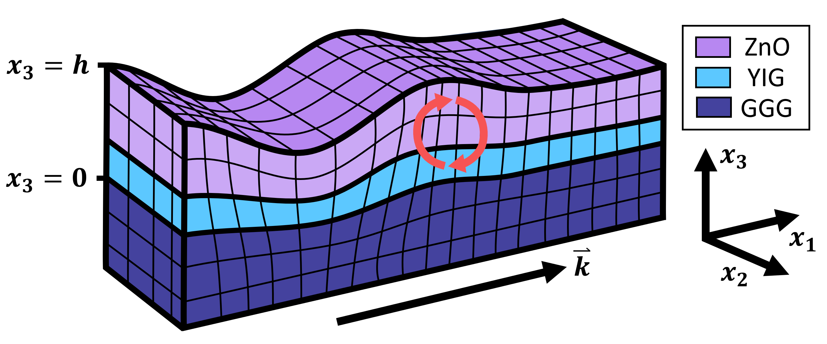
To begin, we present the analytical model used to determine the SAW dispersion relation in a thin-film structure consisting of -layers. The methodology follows that laid out by Farnell and Adler [40]; however, we consider it valuable to present it here in some detail to aid in the comparison between the model and our experimental results. We consider the model a useful tool to obtain fairly accurate analytical results in just a few minutes, without the need to resort to computationally intensive finite-element modeling. The relevant geometry of the thin-film layered structures can be seen in Fig. 1, where we show a YIG/ZnO two-layer thin film structure on a Gadolinium Gallium Garnet (GGG) substrate. is the direction normal to the surface, with the interface between the first layer and the substrate at , and a total YIG/ZnO film layer thickness given by . The GGG substrate is assumed to extend to in the direction. The waves propagate in the direction.
For a piezoelectric material, such as ZnO, the equations of motion are given by
| (1) |
where are the mechanical displacements, the electric potential, the density, and , and the elastic, piezoelectric, and permittivity tensors respectively.
As we are looking for SAWs, we propose the ansatz
| (2) |
where we have a wave of amplitude propagating in the direction with wavenumber and phase velocity . The exponentially decaying component in the direction, with complex coefficient , gives the SAW characteristic. Substituting this ansatz into the equations of motion yields the Christoffel equation
| (3) | |||
are given by quadratic equations in with components of the elastic, piezoelectric, and permittivity tensors as the coefficients.
For a nontrivial solution, the determinant of the matrix in eq. (3) must be zero; therefore, for each value of , there is an eighth-order polynomial in to solve. The amplitude coefficients, , can then be found by solving eq. (3) for each solution of ; giving a solution that is a superposition of partial waves
| (4) |
rather than the monochromatic wave ansatz in eq. (2).
As we are considering thin layers, where the wavelengths are comparable to the thicknesses, all the solutions of are taken, such that the index runs from 1 to 8. However, in the substrate, only the in the lower half of the complex plane are considered, as the wave must vanish as , hence the index runs from 1 to 4. Therefore, in total, the index runs from 1 to 8(number of layers)+4.
The solutions found thus far only give the relations between , , and . As we are interested in the dispersion relations, we must additionally consider the boundary conditions. To do so, we use the linearised coupled strain-charge equations
| (5) |
where is the stress tensor, the strain tensor, the electric field, and the electric displacement with
| (6) |
At each layer interface, , , , , , and are continuous, giving 8 boundary condition equations. At the free surface, there is no restriction on the mechanical displacements, while the same three stress components are zero, and is again continuous; giving four boundary condition equations. Therefore, in total, there are 8(number of layers)+4 boundary condition equations.
Substituting eq. (4) into the boundary condition equations, gives linear equations in the relative amplitudes , and hence can be written in the form of a matrix equation
| (7) |
where is the boundary condition matrix and the index runs over the boundary condition equations. As before, for nontrivial solutions, the determinant of must be zero. Solving this equation gives the phase velocity of the structures in terms of the wavenumber, from which the dispersion relation and group velocity can be easily determined.
In addition, the electromechanical coupling coefficients, given by [41]
| (8) |
can be calculated. Where is the phase velocity previously calculated, and is the phase velocity calculated with an infinitesimally thin perfect conductor layer at the position of the IDT. This metallic film modifies the boundary conditions such that the electric potential, , at the conductor is zero. If the film is on the free surface, the size of the boundary condition matrix is unchanged; whereas, in the case of an interlayer IDT, an additional 8 equations must be added. gives an estimate of the conversion efficiency between electrical and acoustic energy.
III Sample structuring
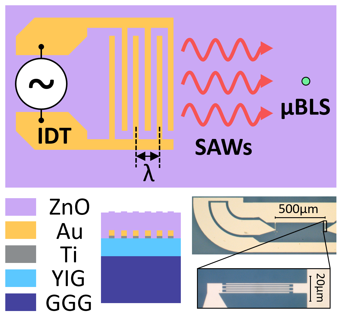
Before examining the results of the analytical model, we first discuss the sample preparation and structuring. A schematic of the sample structure and a microscope image of one of the IDTs can be seen in Fig. 2. Experimental results from two samples are presented here and the thicknesses of the layers and IDTs can be found in Tab. 1.
| Sample | GGG | YIG | IDT | ZnO | |
|---|---|---|---|---|---|
| Ti | Au | ||||
| Sample 1 | 0.5mm | 103nm | 10nm | 80nm | 890nm |
| Sample 2 | 0.5mm | 55nm | 10nm | 80nm | 830nm |
The YIG thin films were grown by liquid phase epitaxy on a (111) oriented GGG substrate [42]. The 103 nm film was purchased commercially from the company Matesy GmbH in Jena, Germany, and the 55 nm film was grown at INNOVENT e.V., Germany. To reach sufficiently high frequencies to enable the future study of SAW-SW coupling, electron beam lithography was used to pattern IDTs with 6 and 20-fingers with finger widths and separations of 700 nm ( 2.8 m), and an aperture size of 50 m. The titanium-gold stack was deposited by electron beam evaporation, followed by a lift-off process to leave behind the IDT. The ZnO was RF magnetron sputtered over the entire sample, with the piezoelectric c-axis of the wurtzite crystal structure pointing out-of-plane. Finally, the contact pads of the IDTs were etched free of the insulating ZnO using hydrochloric acid. A more detailed description of this process, including x-ray diffraction (XRD) characterisation, can be found in the Supplemental Material [43].
IV Experimental methods
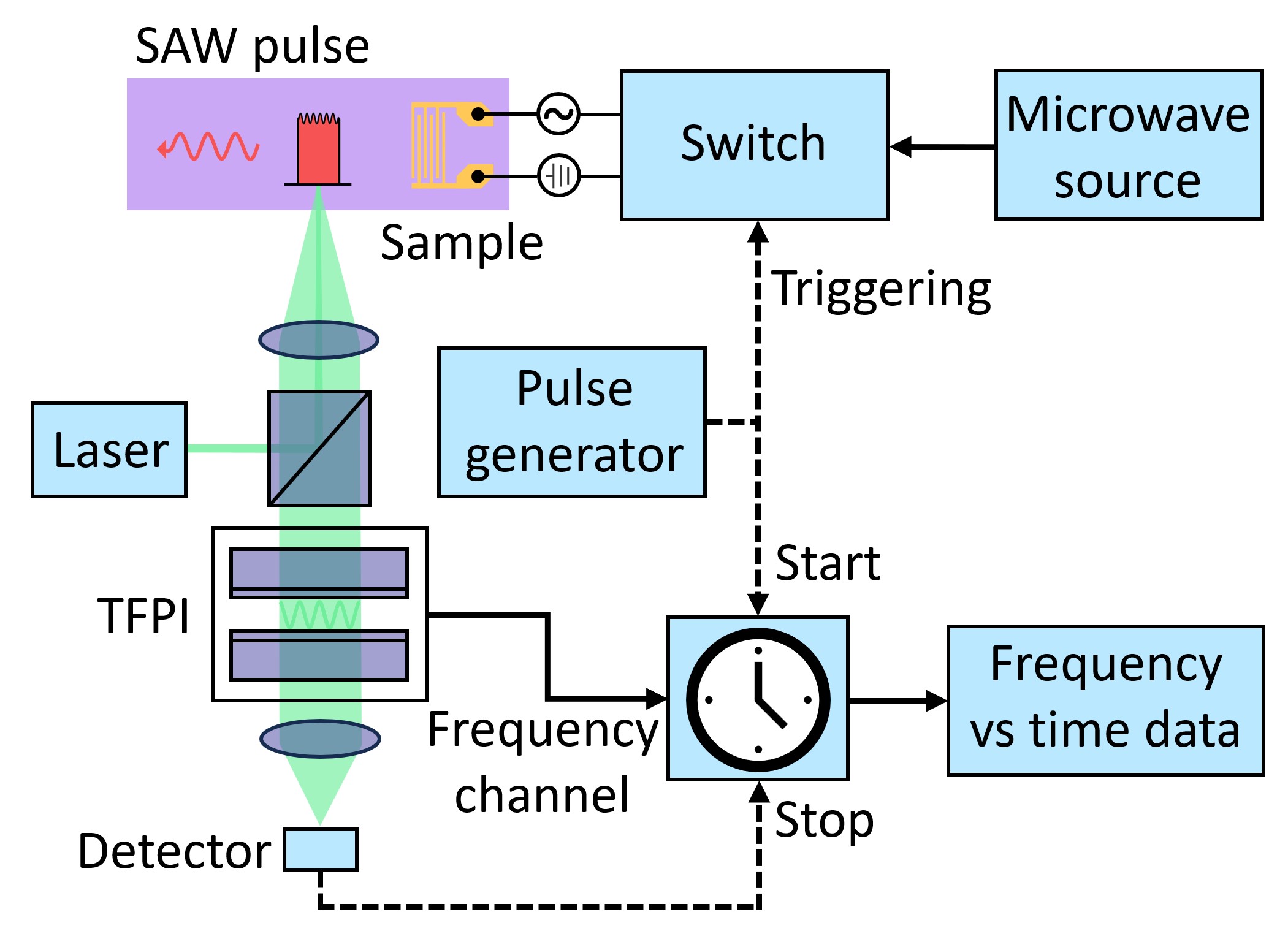
To excite SAWs, the IDT is contacted using a microwave probe with a ground-signal-ground footprint and pitch of 200 m, connected to a microwave source and an amplifier. The IDT is directly excited and the SAW intensity is measured using -BLS [44, 45, 46], with a 532 nm wavelength laser, to determine the IDT’s frequency response. A schematic of this set-up can be seen in Fig. 2. Note, a half-wave plate is used to suppress possible magnon-induced signals by their polarization-dependence [21].
In addition to standard -BLS measurements, we also take time-resolved data to find the phonon group velocities. A schematic of the time-resolved -BLS setup is shown in Fig. 3. A pulse generator is used to trigger a -BLS measurement window, during this window a microwave switch is opened for approximately 600 ns, allowing a microwave pulse of fixed frequency to excite the IDT.
V Analytical results
Considering the above sample structures, we calculated the dispersion relations following the methodology laid out in Section II. This requires a large number of material parameters, as discussed below, and there are no free parameters in the calculation, as such, an exact solution is numerically converged upon. Practically, we propose an initial guess for at a fixed , and if a solution for is converged upon, continue to make small steps in over a predefined range finding .
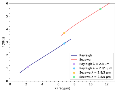
The resulting dispersion relation for Sample 1 can be seen in Fig. 4a. Solving the wave equation leads to multiple solutions, which can be grouped into two classes depending on the type of particle displacement induced. The first are ‘Rayleigh modes’, which result in an elliptical particle motion in the , plane for the case of isotropic materials [48, 40], as shown schematically in Fig. 1 by the red arrows. We note that due to the anisotropic layered structures, there is additional particle motion as discussed in the Supplemental Material [43], hence we use the term ‘Rayleigh-like’. The zeroth-order mode, shown by the dark blue line in Fig. 4a, always exists in the structure; however, the higher-order ‘Sezawa’ modes are only introduced when the shear wave speed in the layer exceeds that of the substrate [49]. The first-order Sezawa-like mode is shown by the red line in Fig. 4a.
The second class of solutions are ‘Love modes’, which have particle motion perpendicular to the direction of propagation for isotropic materials [50]. In the case of our layered structures, we find the expected excitation frequencies of the Love-like modes to be similar to those of the Rayleigh-like modes, thus prohibiting their differentiation with BLS frequency response data due to the finite linewidths. However, the difference between the Rayleigh and Love-like modes is significantly more pronounced when considering the group velocity curves. We did not find the calculated group velocity curves for the Love-like modes to fit well with the experimental data, and therefore, chose to ignore this class of solutions. This is presumably owing to the small electromechanical coupling coefficients calculated for these modes, typically two orders of magnitude smaller than those of the Rayleigh-like modes, another reason we chose to ignore these solutions.
It is important to note a few caveats relating to our methodology: firstly, the IDTs, in particular their finite thickness, are neglected in the simple analytical model; secondly, as mentioned, literature values for the density and elastic, piezoelectric, and permittivity tensors are used for the ZnO [41], YIG [51, 52], and GGG [53, 54] as listed in the Supplemental Material [43], rather than measured values for our films. As this results in a total of 23 material parameters used in the model, generally measured in bulk samples, we do not attempt to estimate an error in the analytical calculation.
Thirdly, based on our experience of growing ZnO films sputtered under near identical conditions, we expect there to be an approximately 200 nm ‘dead layer’ of ZnO where the c-axis is not aligned [55]. This layer occurs as the ZnO does not begin growth with an aligned c-axis, instead growing with a random orientation that begins to self-texture, preferentially forming out-of-plane c-axis aligned columnar grains. To account for this, we introduce an additional 200 nm layer between the YIG and the c-axis aligned ZnO, which we treat as polycrystalline ZnO with randomly oriented c-axes - calculating the material constants accordingly [56]. Physically, we expect a gradual increase in c-axis alignment from the initial complete randomisation; however, we consider the simple model to be adequate as a first-order approximation given the observed change in the dispersion relation is minor. The only sizeable effect is a reduction in the electromechanical coupling coefficients by one to two orders of magnitude, depending on frequency. This is expected, given the electrical excitation from the embedded IDTs is concentrated around this ‘dead layer’ where there is no macroscopic alignment of electric dipoles. Indeed, improving c-axis alignment and reducing the ‘dead layer’ thickness is the key to improved excitation efficiency and an area of active research. We consider these three caveats to be the most likely source of any discrepancies between analytical and experimental results; although, as will be shown, these are relatively small.
Further discussion of the model of the ‘dead layer’, the rotation of crystallographic axes including the ZnO piezoelectric c-axis, and calculations of the coupling coefficients, and normalised mechanical displacements and strains may be found in the Supplemental Material [43].
VI Experimental Results
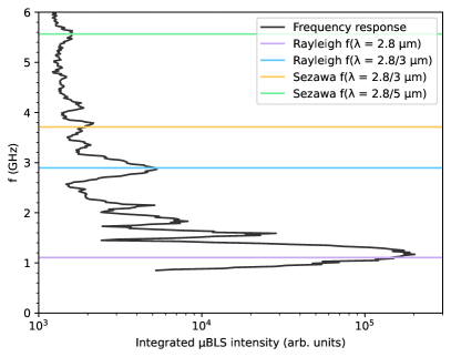
First, we measured the frequency response of the 6-finger IDT on Sample 1 and compared this to the expected excitation frequencies from the analytical calculation. This comparison is shown in Fig. 4b. To maximise the signal, the laser spot was positioned centrally relative to the IDT aperture and approximately 1 m along the SAW propagation path. We expect the highest intensity peak to correspond to the fundamental frequency which is determined by the periodicity/ wavelength of the IDT (2.8 m) according to . Moreover, we should see higher order modes corresponding to where is an odd integer - a net electric field between IDT fingers is required to excite a SAW. We see the fundamental frequency occurs at approximately 1.1 GHz. The coloured horizontal lines indicate the calculated excitation frequencies of the IDT and show good agreement with the peaks in the experimental data.
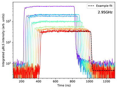
Second, we used time-resolved measurements to calculate the phonon group velocities at fixed microwave frequencies. An example of the resultant BLS intensity as a function of time can be seen in Fig. 5a. We see top-hat-like intensity profiles, where high intensities correspond to the presence of a SAW at the laser spot position. The laser spot is initially positioned centrally next to the IDT and then moved away from the IDT along the SAW propagation direction in equal-sized steps. At each step, a BLS measurement is taken corresponding to the different coloured lines from purple to red in Fig. 5a. This data is then fitted using a least squares regression with the sigmoidal Boltzmann function to smoothly approximate the Heaviside step function
| (9) |
where is the BLS intensity, is the time, and , , , and are constants. An example fit is shown by the black dotted curve fitting the red BLS data.
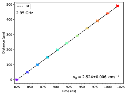
From these fits we extract the constant , the position of the falling edge of the SAW pulse, with an associated fitting error. Combining this with the known laser spot position, we can plot the SAW propagation distance from the IDT as a function of , Fig. 5b. Alongside the fitting error in , we take into account experimental errors of 2 ns for time-based measurements and 1 m for the microscope position stabilisation. A straight line is fitted to the data, using orthogonal distance regression, to determine the group velocity at a fixed frequency.
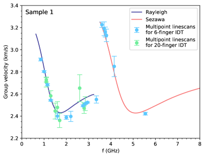
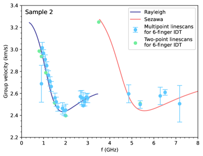
The results of this fitting process can be seen for Sample 1 in Fig. 5c and Sample 2 in Fig. 5d. We show the experimentally determined group velocities with their associated errors in light blue and green as a function of the SAW excitation frequency. For Sample 1, the group velocities were measured for two IDT structures, one with 6-fingers, light blue, and the other with 20-fingers, green. These group velocities were determined from multipoint linescans, that is to say, the laser spot was scanned over multiple points in space, as in Fig. 5a. For Sample 2, all measurements were made on the same 6-finger IDT. In light blue, we again have group velocities determined from multipoint linescans. In green, however, the group velocities were calculated from two-point linescans, where the laser spot was positioned at only two points in space, one next to the IDT and the other at the maximum distance measured from the IDT of 500 m. There is good agreement between the two-point and multipoint measurements showing the accuracy of the technique.
Figs 5c and 5d also show the analytically calculated group velocities of the Rayleigh-like mode in dark blue and the Sezawa-like mode in red for Sample 1 (Fig 5c) and Sample 2 (Fig 5d). Given the caveats discussed in Section V, the agreement between the analytical model and the experimental data is excellent, with the largest discrepancies, in general, occurring for the points with the largest measurement errors. These large errors occur due to the low excitation efficiency of the IDT at these frequencies, meaning the top-hat-like intensity profiles become more noisy. In particular, the narrower bandwidth 20-finger IDT tends to show larger errors when off-resonance, as expected. In general, the data fits the curvature well and we can differentiate between the Rayleigh and Sezawa-like modes. These results show we can measure the non-linearity in the phonon dispersion relation for these complex layered structures to a high accuracy using time-resolved -BLS. Furthermore, we demonstrate good agreement with the analytical model, thus verifying the model is sufficient within the assumptions made to interpret our experimental data. Additionally, the experimental results agree with the model for two different samples and three different IDT structures with different ZnO and YIG thicknesses.
Finally, from the amplitudes of the top-hat-like functions found from the Boltzmann fits, we can estimate the phonon decay length by fitting the equation
| (10) |
where is the initial amplitude and the decay length. Due to the aforementioned reduction in experimental data quality when off-resonance, we only calculate this decay length for values near the first accessible harmonic frequency of the IDT. Taking a weighted average, we find a decay length of for the 6-finger IDT on Sample 1, consistent with the value of for the 6-finger IDT on Sample 2. We believe the relatively large errors in these values result from variations in the reflectivity of the surface of the samples, which could result from defects in the film or surface particles. We note that etching away the ZnO along the propagation path after the excitation region may increase the decay length, given the ‘dead layer’ is not crystallographically ordered, and therefore, will have increased scattering.
VII Conclusion and outlook
In conclusion, we have demonstrated a method to generate gigahertz frequency SAWs in YIG thin films by first patterning IDTs on the surface of the YIG, and then sputter depositing thin films of piezoelectric ZnO. We measured the IDT frequency responses and SAW group velocities of these structures experimentally using time-resolved -BLS. Using these experimental results, we show good agreement with an analytical model that calculates the dispersion relation of the SAWs in these thin film heterostructures. We are able to differentiate between Rayleigh and Sezawa-like modes.
We hope this work lays the foundations for the study of the SAW-SW interaction in YIG, with the possibility of observing non-reciprocal SW generation, and therefore, probing device ideas such as acoustic isolators or circulators [9, 12, 14]. With efficient SAW excitation, there is additionally the prospect of studying strong magnon-phonon coupling [57] and non-linear SAW-SW interaction phenomena [58, 59]. Furthermore, the successful deposition of piezoelectric ZnO, despite the large lattice mismatch with YIG [60, 61], suggests it may be possible to similarly excite SAWs in other lattice mismatched thin film materials. This demonstrates the versatility of using ZnO as a piezoelectric and possibly opens the door to studying the magnetoacoustic interaction in additional magnetic media.
Acknowledgements.
This work was supported by the European Research Council (ERC) under the European Union’s Horizon Europe research and innovation programme (Consolidator Grant “MAWiCS”, Grant Agreement No. 101044526). The work of F. Ryburn was supported by a UK Engineering and Physical Sciences Research Council (EPSRC) Industrial Cooperative Award in Science & Technology. The work of M. Linder was supported by the German Bundesministerium für Wirtschaft und Energie 262 (BMWi) under Grant No. 49MF180119.References
- Campbell [1998] C. Campbell, Surface Acoustic Wave Devices for Mobile and Wireless Communications, Four-Volume Set (Academic press, 1998).
- Ruby [2015] R. Ruby, IEEE Microwave Magazine 16, 46 (2015).
- Gronewold [2007] T. M. Gronewold, Analytica Chimica Acta 603, 119 (2007).
- Mandal and Banerjee [2022] D. Mandal and S. Banerjee, Sensors 22 (2022), 10.3390/s22030820.
- Wohltjen [1984] H. Wohltjen, Sensors and Actuators 5, 307 (1984).
- Parker and Montress [1988] T. Parker and G. Montress, IEEE Transactions on Ultrasonics, Ferroelectrics, and Frequency Control 35, 342 (1988).
- Ding et al. [2013] X. Ding, P. Li, S.-C. S. Lin, Z. S. Stratton, N. Nama, F. Guo, D. Slotcavage, X. Mao, J. Shi, F. Costanzo, et al., Lab on a Chip 13, 3626 (2013).
- Destgeer and Sung [2015] G. Destgeer and H. J. Sung, Lab on a Chip 15, 2722 (2015).
- Sasaki et al. [2017] R. Sasaki, Y. Nii, Y. Iguchi, and Y. Onose, Phys. Rev. B 95, 020407(R) (2017).
- Tateno and Nozaki [2020] S. Tateno and Y. Nozaki, Phys. Rev. Appl. 13, 034074 (2020).
- Hernández-Mínguez et al. [2020] A. Hernández-Mínguez, F. Macià, J. M. Hernàndez, J. Herfort, and P. V. Santos, Phys. Rev. Appl. 13, 044018 (2020).
- Xu et al. [2020] M. Xu, K. Yamamoto, J. Puebla, K. Baumgaertl, B. Rana, K. Miura, H. Takahashi, D. Grundler, S. Maekawa, and Y. Otani, Science Advances 6, eabb1724 (2020).
- Küß et al. [2020] M. Küß, M. Heigl, L. Flacke, A. Hörner, M. Weiler, M. Albrecht, and A. Wixforth, Phys. Rev. Lett. 125, 217203 (2020).
- Küß et al. [2021a] M. Küß, M. Heigl, L. Flacke, A. Hefele, A. Hörner, M. Weiler, M. Albrecht, and A. Wixforth, Phys. Rev. Appl. 15, 034046 (2021a).
- Küß et al. [2021b] M. Küß, M. Heigl, L. Flacke, A. Hörner, M. Weiler, A. Wixforth, and M. Albrecht, Phys. Rev. Appl. 15, 034060 (2021b).
- Li et al. [2021] Y. Li, C. Zhao, W. Zhang, A. Hoffmann, and V. Novosad, APL Materials 9, 060902 (2021).
- Geilen et al. [2022a] M. Geilen, A. Nicoloiu, D. Narducci, M. Mohseni, M. Bechberger, M. Ender, F. Ciubotaru, B. Hillebrands, A. Müller, C. Adelmann, and P. Pirro, Applied Physics Letters 120, 242404 (2022a).
- Küß et al. [2023a] M. Küß, M. Hassan, Y. Kunz, A. Hörner, M. Weiler, and M. Albrecht, Phys. Rev. B 107, 024424 (2023a).
- Küß et al. [2023b] M. Küß, M. Hassan, Y. Kunz, A. Hörner, M. Weiler, and M. Albrecht, Phys. Rev. B 107, 214412 (2023b).
- Huang et al. [2023] M. Huang, W. Hu, H. Zhang, and F. Bai, Journal of Applied Physics 133, 223902 (2023).
- Kunz et al. [2023] Y. Kunz, M. Küß, M. Schneider, M. Geilen, P. Pirro, M. Albrecht, and M. Weiler, arXiv preprint arXiv:2311.16688 (2023), arXiv:2311.16688 .
- Shah et al. [2020] P. J. Shah, D. A. Bas, I. Lisenkov, A. Matyushov, N. X. Sun, and M. R. Page, Science Advances 6, eabc5648 (2020).
- Verba et al. [2021] R. Verba, E. N. Bankowski, T. J. Meitzler, V. Tiberkevich, and A. Slavin, Advanced Electronic Materials 7, 2100263 (2021).
- Rasmussen et al. [2021] C. Rasmussen, L. Quan, and A. Alù, Journal of Applied Physics 129, 210903 (2021).
- Küß et al. [2022] M. Küß, M. Albrecht, and M. Weiler, Frontiers in Physics 10 (2022), 10.3389/fphy.2022.981257.
- Li et al. [2017] X. Li, D. Labanowski, S. Salahuddin, and C. S. Lynch, Journal of Applied Physics 122, 043904 (2017).
- Mahmoud et al. [2020] A. Mahmoud, F. Ciubotaru, F. Vanderveken, A. V. Chumak, S. Hamdioui, C. Adelmann, and S. Cotofana, Journal of Applied Physics 128, 161101 (2020).
- Chumak et al. [2022] A. V. Chumak, P. Kabos, M. Wu, C. Abert, C. Adelmann, A. Adeyeye, J. Åkerman, F. G. Aliev, A. Anane, A. Awad, et al., IEEE Transactions on Magnetics 58, 1 (2022).
- Rana et al. [2017] B. Rana, Y. Fukuma, K. Miura, H. Takahashi, and Y. Otani, Applied Physics Letters 111, 052404 (2017).
- Nikitchenko and Pertsev [2021] A. I. Nikitchenko and N. A. Pertsev, Phys. Rev. B 104, 134422 (2021).
- Qin et al. [2018] H. Qin, S. J. Hämäläinen, K. Arjas, J. Witteveen, and S. van Dijken, Phys. Rev. B 98, 224422 (2018).
- Maendl et al. [2017] S. Maendl, I. Stasinopoulos, and D. Grundler, Applied Physics Letters 111, 012403 (2017).
- Koike et al. [1993] J. Koike, K. S. K. Shimoe, and H. I. H. Ieki, Japanese Journal of Applied Physics 32, 2337 (1993).
- Le Brizoual et al. [2008] L. Le Brizoual, F. Sarry, O. Elmazria, P. Alnot, S. Ballandras, and T. Pastureaud, IEEE Transactions on Ultrasonics, Ferroelectrics, and Frequency Control 55, 442 (2008).
- Wang et al. [2008] Q. J. Wang, C. Pflügl, W. F. Andress, D. Ham, F. Capasso, and M. Yamanishi, Journal of Vacuum Science & Technology B: Microelectronics and Nanometer Structures Processing, Measurement, and Phenomena 26, 1848 (2008).
- Fu et al. [2019] S. Fu, W. Wang, L. Qian, Q. Li, Z. Lu, J. Shen, C. Song, F. Zeng, and F. Pan, IEEE Electron Device Letters 40, 103 (2019).
- Su et al. [2020] R. Su, S. Fu, J. Shen, Z. Chen, Z. Lu, M. Yang, R. Wang, F. Zeng, W. Wang, C. Song, et al., ACS Applied Materials & Interfaces 12, 42378 (2020).
- Hanna and Murphy [1988] S. Hanna and G. Murphy, IEEE Transactions on Magnetics 24, 2814 (1988).
- Kryshtal and Medved [2017] R. Kryshtal and A. Medved, Journal of Physics D: Applied Physics 50, 495004 (2017).
- FARNELL and ADLER [1972] G. FARNELL and E. ADLER (Academic Press, 1972) pp. 35–127.
- Zhang [2022] G. Zhang, Bulk and Surface Acoustic Waves (CRC Press, 2022).
- Dubs et al. [2020] C. Dubs, O. Surzhenko, R. Thomas, J. Osten, T. Schneider, K. Lenz, J. Grenzer, R. Hübner, and E. Wendler, Phys. Rev. Mater. 4, 024416 (2020).
- [43] See Supplemental Material for information about sample preparation; material parameters used in calculations; calculations of the electromechanical coupling coefficients, displacements, and strains; rotation of crystallographic axes including the piezoelectric ZnO c-axis; and the modelling of the ‘dead layer’, which includes Refs. [62, 63, 64, 41, 51, 52, 53, 54, 40, 13, 55, 56, 65, 66, 67, 68, 69].
- Büttner et al. [2000] O. Büttner, M. Bauer, S. O. Demokritov, B. Hillebrands, Y. S. Kivshar, V. Grimalsky, Y. Rapoport, M. P. Kostylev, B. A. Kalinikos, and A. N. Slavin, Journal of Applied Physics 87, 5088 (2000).
- Demidov et al. [2004] V. E. Demidov, S. O. Demokritov, B. Hillebrands, M. Laufenberg, and P. P. Freitas, Applied Physics Letters 85, 2866 (2004).
- Sebastian et al. [2015] T. Sebastian, K. Schultheiss, B. Obry, B. Hillebrands, and H. Schultheiss, Frontiers in Physics 3 (2015).
- Heinz [2021] B. M. Heinz, Nano-scaled yttrium iron garnet conduits for magnonic networks, Ph.D. thesis, Rheinland-Pfälzische Technische Universität Kaiserslautern-Landau (2021).
- Rayleigh [1885] L. Rayleigh, Proceedings of the London mathematical Society 1, 4 (1885).
- Sezawa [1927] K. Sezawa, Bull. Earthq. Res. Inst. Tokyo 3, 1 (1927).
- Love [1911] A. E. H. Love, Some Problems of Geodynamics: Being an Essay to which the Adams Prize in the University of Cambridge was Adjudged in 1911 (University Press, 1911).
- Clark and Strakna [2004] A. E. Clark and R. E. Strakna, Journal of Applied Physics 32, 1172 (2004).
- Hasan et al. [2017] I. H. Hasan, M. N. Hamidon, I. Ismail, R. Osman, and A. Ismail, in 2017 IEEE Regional Symposium on Micro and Nanoelectronics (RSM) (2017) pp. 131–134.
- Graham and Chang [2003] L. J. Graham and R. Chang, Journal of Applied Physics 41, 2247 (2003).
- Connelly et al. [2021] D. A. Connelly, H. R. O. Aquino, M. Robbins, G. H. Bernstein, A. Orlov, W. Porod, and J. Chisum, IEEE Magnetics Letters 12, 1 (2021).
- Fung [2015] T. Fung, Phonon magnonics, Ph.D. thesis, University of Oxford (2015).
- Den Toonder et al. [1999] J. Den Toonder, J. Van Dommelen, and F. Baaijens, Modelling and Simulation in Materials Science and Engineering 7, 909 (1999).
- Hwang et al. [2023] Y. Hwang, J. Puebla, K. Kondou, C. Gonzalez-Ballestero, H. Isshiki, C. S. Munoz, L. Liao, F. Chen, W. Luo, S. Maekawa, et al., arXiv preprint arXiv:2309.12690 (2023), arXiv:2309.12690 .
- Geilen et al. [2022b] M. Geilen, R. Verba, A. Nicoloiu, D. Narducci, A. Dinescu, M. Ender, M. Mohseni, F. Ciubotaru, M. Weiler, A. Müller, B. Hillebrands, C. Adelmann, and P. Pirro, “Parametric excitation and instabilities of spin waves driven by surface acoustic waves,” (2022b), arXiv:2201.04033 .
- Shah et al. [2023] P. J. Shah, D. A. Bas, A. Hamadeh, M. Wolf, A. Franson, M. Newburger, P. Pirro, M. Weiler, and M. R. Page, “Symmetry and nonlinearity of spin wave resonance excited by focused surface acoustic waves,” (2023), arXiv:2305.06259 .
- Abrahams and Bernstein [1969] S. C. Abrahams and J. L. Bernstein, Acta Crystallographica Section B 25, 1233 (1969).
- Gurjar et al. [2019] G. Gurjar, V. Sharma, S. Patnaik, and B. K. Kuanr, AIP Conference Proceedings 2115, 030323 (2019).
- Bachari et al. [1999] E. Bachari, G. Baud, S. Ben Amor, and M. Jacquet, Thin Solid Films 348, 165 (1999).
- Lin and Huang [2004] S.-S. Lin and J.-L. Huang, Surface and Coatings Technology 185, 222 (2004).
- Howe et al. [2015] B. M. Howe, S. Emori, H.-M. Jeon, T. M. Oxholm, J. G. Jones, K. Mahalingam, Y. Zhuang, N. X. Sun, and G. J. Brown, IEEE Magnetics Letters 6, 1 (2015).
- Foster et al. [1968] N. Foster, G. Coquin, G. Rozgonyi, and F. Vannatta, IEEE Transactions on Sonics and Ultrasonics 15, 28 (1968).
- Yanagitani et al. [2011] T. Yanagitani, N. Morisato, S. Takayanagi, M. Matsukawa, and Y. Watanabe, IEEE Transactions on Ultrasonics, Ferroelectrics and Frequency Control 58 (2011).
- Laude and Ballandras [2003] V. Laude and S. Ballandras, Journal of Applied Physics 94, 1235 (2003).
- O’Rorke et al. [2020] R. O’Rorke, A. Winkler, D. Collins, and Y. Ai, RSC advances 10, 11582 (2020).
- Maupin [2007] V. Maupin, in Advances in Wave Propagation in Heterogenous Earth, Advances in Geophysics, Vol. 48, edited by R.-S. Wu, V. Maupin, and R. Dmowska (Elsevier, 2007) pp. 127–155.