[1,2]\fnmRounak \surJha [1]\fnmParitosh \surKarnatak
[1]\orgdivDepartment of Physics, \orgnameUniversity of Basel, \orgaddress\cityCH-4056 Basel, \countrySwitzerland
2]\orgdivLaboratory of Quantum Physics (LQP), \orgnameÉcole Polytechnique Fédérale de Lausanne (EPFL), \orgaddress\cityCH-1015 Lausanne, \countrySwitzerland
3]\orgdivResearch Center for Functional Materials, \orgnameNational Institute for Material Science, \orgaddress\streetStreet, \city1-1 Namiki, \stateTsukuba 305-0044, \countryJapan
4]\orgdivInternational Center for Materials Nanoarchitectonics, \orgnameNational Institute for Material Science, \orgaddress\streetStreet, \city1-1 Namiki, \stateTsukuba 305-0044, \countryJapan
5]\orgdivSwiss Nanoscience Institute, \orgnameUniversity of Basel, \orgaddress\cityBasel, \postcode4056, \countrySwitzerland
Large tunable kinetic inductance in a twisted graphene superconductor
Abstract
Twisted graphene based moiré heterostructures host a flat band at the magic angles where the kinetic energy of the charge carriers is quenched and interaction effects dominate. This results in emergent phases such as superconductors and correlated insulators that are electrostatically tunable. We investigate superconductivity in twisted trilayer graphene (TTG) by integrating it as the weak link in a superconducting quantum interference device (SQUID). The measured current phase relation (CPR) yields a large and tunable kinetic inductance, up to 150 nH per square, of the electron and hole type intrinsic superconductors. We further show that the specific kinetic inductance and the critical current density are universally related via the superconducting coherence length, and extract an upper bound of nm for the coherence length. Our work opens avenues for using graphene-based superconductors as tunable elements in superconducting circuits.
keywords:
superconductivity, moiré, kinetic inductance, grapheneThe discovery of novel phases, such as superconductors and correlated insulators, that emerge in a few atomic layers of twisted graphene has brought a new class of materials to the fore [1, 2, 3, 4, 5, 6, 7, 8]. While graphene by itself is a semi-metal, twisted graphene systems host an emergent flat band at the magic angles where the kinetic energy of the charge carriers is small and interactions dominate. Such strong electron-electron correlations lead to a spontaneous breaking of the underlying symmetries and several phases manifest from the ensuing competition between various ground states [1, 2, 3, 5]. The superconducting phase is particularly interesting and many studies point to a departure from a Bardeen–Cooper–Schrieffer (BCS) origin of the superconductivity [2, 9, 5, 7, 10]. Moreover, as this rich phase diagram is accessible by electrostatic tuning, these materials have been used to design novel superconducting devices [11, 12].
Currently, superconducting circuits are widely utilised to design well defined quantum states and control circuits at the mesoscopic scale to create one of the leading quantum bit (qubit) architectures [13, 14, 15]. A key fundamental property of the superconductors is called the kinetic inductance, that arises from the inertia of Cooper pairs and is proportional to the ratio of the effective mass of the charge carriers and the superfluid density. Recently, high kinetic inductance superconductors, such as TiN [16], NbN [17, 18], NbTiN [19, 20] and granular aluminum [21, 22], have been utilised in superconducting circuits, for example, to design novel qubits [23], to achieve a strong qubit-photon coupling [24, 25, 26, 27] as well as in applications such as sensitive photon detectors [28, 29, 30] and cryogenic amplifiers [31, 32]. However, the kinetic inductance of such disordered superconducting films is typically limited to nH [30]. On the other hand, in moiré flat band materials a large tunable kinetic inductance is expected [33], owing to a large effective mass of the charge carriers and a tunable, low charge carrier density ( m-2).
In this work, we investigate superconductivity in twisted trilayer graphene (TTG), by integrating it as the weak link in a SQUID (superconducting quantum interference devices) loop of superconducting molybdenum rhenium (MoRe). We show that, in the intrinsic superconducting regimes, the phase winds like a linear inductor across the TTG weak link and contrast this with the proximity superconducting regime where TTG exhibits a sinusoidal current phase relation (CPR). For the superconducting TTG we measure a large kinetic inductance, up to 150 nH which is electrostatically tunable. Moreover, by studying the kinetic inductance of the superconducting phase as a function of the critical current density we extract the upper bounds of 200 nm and 190 nm for the superconducting coherence lengths in the electron and the hole type flat bands, respectively. Finally, with a critical current density of nA/m we show that graphene-based superconductors may be promising as tunable elements in superconducting circuits.
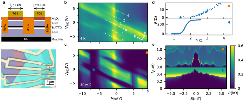
We create the TTG by twisting three layers of graphene, such that the top and the bottom layers are aligned while the middle layer is twisted at an angle . TTG is encapsulated between hexagonal Boron Nitride (hBN) layers with graphite underneath which functions as the backgate (BG). The schematic shown in Fig. 1(a) (top) represents the cross section of a device along the dashed black line in the optical image shown at the bottom. The edge contacts to twisted trilayer graphene are made by etching the structure and then sputtering nm MoRe. MoRe also forms the superconducting loop for the SQUID. Finally, nm Al2O3 is grown using atomic layer deposition and Ti/Au topgates are fabricated on top of each TTG weak link for individual control over the junctions. See methods for further details.
The characteristic transport signatures of twisted trilayer graphene flat bands are shown by the differential resistance map at K by sweeping the backgate voltage () and the topgate voltage () on junction 2 (jn2), while , as shown in Fig.1(b). The dashed white lines mark the resistive features visible at integer fillings of the two flat bands. Here , where is the charge carrier density and is the carrier density at the full filling of the flat bands. Displacement field () dependent resistance peaks are visible at , and yield a twist angle of (Supplementary Information, section I). At mK (Fig. 1c), the zero resistance features dominate and the intrinsic superconductivity of TTG is visible on the electron and the hole side near as well as the proximity superconductivity induced by MoRe at high electron doping, in the upper right corner of Fig. 1c.
The intrinsic and proximity superconducting regions show a marked difference in the vs. plot shown in Fig. 1d. The resistance in the proximity region (orange dot in Fig. 1c) gradually rises, highlighting the weakening proximity effect with increasing temperature. The intrinsic TTG superconductor (blue diamond in Fig. 1c), on the other hand, shows a Berezinskii–Kosterlitz–Thouless (BKT) like transition to the normal state typical of 2D superconductors [34, 6, 7]. Furthermore, as shown in Fig. 1e, the proximity superconductor shows a Fraunhofer-like interference in magnetic field [35], while the intrinsic superconductor screens the external magnetic field and the critical current decays monotonically on a larger magnetic field scale [36, 6].
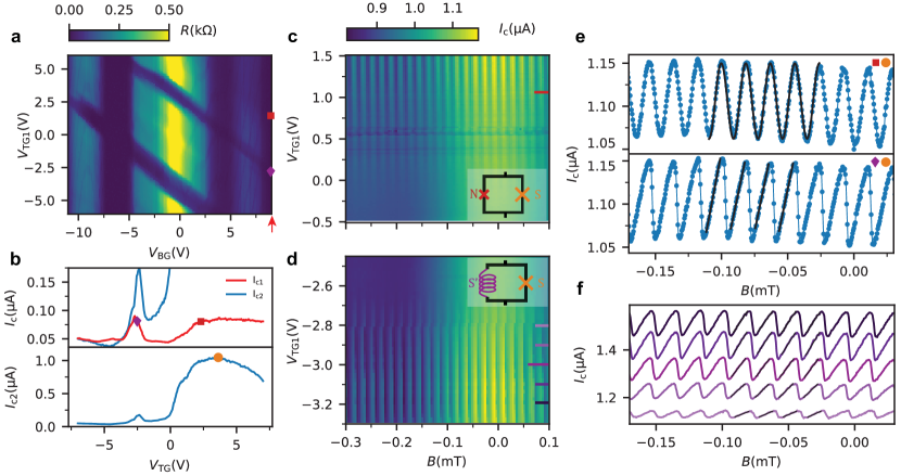
The differential resistance map obtained by sweeping the backgate voltage () and the topgate voltage (), while , is shown in Fig.2a. We measure the switching statistics of the superconducting junctions using a counter (for details see Supplementary Information, section II). The average switching currents for the two junctions are shown, in Fig. 2b, as a function of the respective topgate voltage at fixed V (along the red arrow in Fig. 2a and the blue arrow on Fig. 1c). We notice that the maximum supercurrent of the intrinsic electron type superconductor, at V, in the two junctions differs by a factor (given the zero error in the measurements). This matches well with the ratio of the widths of the two junctions () as would be expected from an intrinsic superconductor. On the other hand, the maximum supercurrents in the proximity regime for the two junctions differ by more than a factor of , highlighting that the superconducting order parameter induced from the MoRe decays exponentially with the junction lengths ( m and m ).
The rich phase diagram for the two TTG junctions allows us to study the SQUID oscillations and probe the current phase relation (CPR) of the weak links in various configurations. The critical current for a weak link is governed by the phase drop across the junction and is given by , where () is the (maximum) critical current, is the phase difference of the superconducting order parameter across the junction and is its CPR, which is typically a periodic function bound to . Since the intrinsic nature of a weak link determines its CPR, measuring the CPR is a valuable probe to access fundamental material properties [37, 33, 38, 39]. For example, the CPR for insulating barriers is sinusoidal [35], that for short junctions of normal materials depends on the transparency of the current carrying modes [40, 41] and a topological weak link generates a sawtooth-like CPR with periodicity [42, 43, 44].
To measure the CPR of junction 1 (jn1), for example, the SQUID can be configured asymmetrically, . This fixes the phase drop across jn2 at the critical phase (phase at which is maximum) resulting in the external flux () essentially tuning the phase drop across jn1. However, an accurate measurement of the CPR requires careful considerations [38, 45]. The frequently used criterion for the SQUID asymmetry, may not be sufficient and the suitable ratio depends on the CPR itself [45]. Moreover, the presence of large inductance effects in the SQUID loop skews the measured CPR [38].
For an accurate measurement of the CPR we keep the ratio and ensure that we observe the expected oscillation amplitude by using the gate tunability of our weak links to eliminate the possibility of large inductance effects from the SQUID loop. We study the CPR of jn1 by fixing jn2 as the reference junction with A, shown by the orange dot in Fig. 2b, and vary across the proximity regime of jn1 (Fig. 2c) and the intrinsic electron type superconductor (Fig. 2d) (see Supplementary Information, section IV for other configurations). The SQUID oscillations in the two regions show a stark contrast, that we better highlight in the two cuts shown in the proximity (Fig. 2e top) and the intrinsic regions (Fig. 2e bottom). For nearly the same critical current nA, the proximitised junction shows a sinusoidal CPR, whereas the same junction when gate tuned into an intrinsic superconductor shows a highly skewed CPR.
The CPR in the proximity regime is sinusoidal (, solid black curve in Fig. 2e) and can be understood by modeling jn1 as a short SNS junction characterised by a small effective transparency 0.5 of the current carrying modes [40, 41] (also see Supplementary Information, section III). In contrast, the SS’S junction formed when TTG is intrinsically superconducting can be modeled as a linear inductor in a simple picture with a supercurrent , where and . In addition, here the periodicity of such an inductor results from the fact that at a critical phase of , where is an integer, it becomes favorable for a vortex to enter the SQUID loop rather than the phase across the intrinsic superconductor (S’) winding further. In fact, vortex generation may be particularly favorable in our two-dimensional superconductor where the magnetic field screening is weak. The SQUID critical current can then be written as
| (1) |
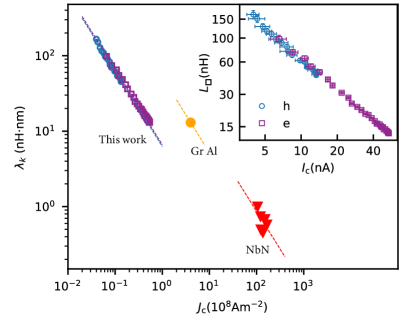
The kinetic inductance of the intrinsic superconductor (jn1) can then be extracted from the slope ( for ) of the rising linear part of the measured CPR. This yields, for example, nH for the bottom panel in Fig. 2e. Multiple such oscillations are shown in Fig. 2f, as is varied from 5 nA to 45 nA by tuning . We see an increase in the slope of the oscillations with increasing indicating a decreasing . The extracted sheet kinetic inductance values, , are shown as a function of for the electron (hole) type intrinsic superconductor as purple squares (blue circles) in a log-log plot in the inset of Fig. 3 (see Supplementary Information, section IV for full measurements). We emphasise that in an intrinsic TTG superconductor we are able to tune the kinetic inductance by more than an order of magnitude from 10 nH to 150 nH, with maximum kinetic inductance values of nH/ for the hole type superconductor, and nH/ for the electron type superconductor.
Using the Ginzburg Landau (GL) theory [35, 47], one can write the critical current density of a superconducting thin film as , under the assumption that , where is the effective mass of electrons ( is the mass of a Cooper pair), is the superfluid density, and is the coherence length. The kinetic inductance on the other hand can be obtained by considering that the total kinetic energy of the Cooper pairs is stored in an inductor (), where is the film thickness and is the supercurrent. Equating the two we obtain the kinetic inductance as .
We then define the specific kinetic inductance as . This yields a universal relation between and that only depends on the coherence length of the superconductor. We note that the contribution of jn.1 towards the critical current of the SQUID, that we obtain from the SQUID oscillations, may be smaller than the critical current predicted from the GL theory. The former is governed by the fluxoid quantisation in the SQUID loop and the phase slip rates in the superconducting thin film, while the latter is related to the vanishing superconducting order parameter of the thin film as the velocity of superconducting charge carriers increases (see Supplementary Information, section VI).
The plot of vs. , shown in Fig. 3, then allows us to extract the upper bound for for the hole ( nm) and the electron type superconductor ( nm) as we tune the critical current density in TTG by tuning the charge carrier density. The estimates of from the switching dynamics of an individual junction further constraint the extracted (see Supplementary Information, section VI).
We emphasise that the coherence length we extract for the twisted trilayer graphene superconductor is larger than those previously reported [6, 7] which places constraints on the nature of superconductivity. Finally, from the available literature we show two other commonly used high kinetic inductance materials, in Fig. 3, namely granular aluminum (Gr Al) [46] and NbN [18], for which we extract nm and nm, respectively, in agreement with the reported values [48].
In the future, it will be intriguing to investigate the kinetic impedance at high frequencies and study other crystalline van der Waals superconductors [49, 50, 51]. Our results demonstrate that twisted trilayer graphene superconductors exhibit a large kinetic inductance up to nH that is tunable by an electric field. They also show a critical current density up to nA/m. And while challenges in terms of the scalability of such materials are outstanding they may compliment the existing elements available for superconducting circuits.
Methods
Fabrication Details
The graphene and hBN flakes are exfoliated on a doped silicon wafer with 285nm of silicon oxide on top (Si/SiO). Large monolayer graphene flakes are selected by optical contrast under a microscope. The graphene flake selected for the device (with dimensions of around 45 m 15 m) is cut into three segments using a tungsten needle controlled with a micromanipulator. For picking up the flakes, we use a polydimethylsiloxane/polycarbonate (PDMS/PC) film. We assemble the stack using a dry pick-up method [52]. First, the top hBN (thickness = nm) flake is picked up with the stage temperature at C. The stage is then cooled down to C to pick up the first (cut) graphene segment, and subsequently rotated by before picking up the second graphene segment. We revert the stage back to to pick up the final graphene flake, such that the first and third graphene layers are aligned. This forms the alternating twist-angle trilayer graphene heterostructure. We encapsulate the TTG by picking up a bottom hBN flake (thickness = nm) at C, before finally picking up a graphite flake, (which serves as the backgate) at C. The stack is deposited by melting the PDMS/PC at C on an undoped Si/SiO substrate. The PDMS/PC film residue is washed away using dichloromethane.
After the preparation of the stack, the regions where MoRe will be deposited as edge contacts are defined using e-beam lithography. We then etch through the top hBN, graphene and a small portion () of the bottom hBN above these regions using reactive ion etching (RIE) (CHF3/O2), before sputtering the MoRe edge contacts ( nm). Subsequently, the graphene junction dimensions are determined by defining an etching mask in another stage of e-beam lithography, which is then etched away with CHF3/O2 RIE. For the next step, we deposit an additional insulating layer in the form of nm Al2O3 using atomic layer deposition (ALD). In the last stage of lithography, the individual togates are fabricated by defining and evaporating Ti/Au ( nm/ nm) above the junction weak links.
Measurement set-up
The transport measurements are done in a dilution refrigerator, which can be cooled down to 30 mK (base temperature). We apply a voltage signal composed of a dc component generated by a voltage source to which a small ac component supplied by a lock-in amplifier is added using a transformer. The signal is converted to a bias current using a 1 M resistor connected in series with the voltage source. The device resistance is determined in a pseudo four-terminal configuration (where we can ignore line resistances but not contact resistances) by measuring the consequent voltage drop across the device on applying the bias current. The lock-in amplifier serves to reduce the signal noise and uses the small ac component (1 to 10 nA) of the signal to measure the differential resistance .
Converting gate voltages to charge carrier densities
To extract the charge carrier densities and the displacement field from the gate voltages, we utilise a parallel plate capacitor model [53].
| (2) |
| (3) |
with
| (4) |
For the topgates, where there are two insulating layers (hBN and Al2O3) separating them from the graphene:
| (5) |
Here, is the gate voltage applied to junction by its corresponding topgate, is the position of the charge neutrality point, and () and () are the dielectric constants and the heights of the corresponding layers. can be non zero due to intrinsic doping of the sample.
Inductance estimation
Our SQUID can be approximated to a rectangular loop, whose geometrical inductance is given by [54]:
| (6) |
where is the height of the loop, is its width, and and are lengths of the two sides of the rectangular loop. We estimate 44pH. Previous studies report the sheet kinetic inductance of MoRe = 4.26 pH [53]. This gives us the kinetic inductance of MoRe in our SQUID loop = 290 pH. The total inductance of these sources is nH, which is much smaller than the extracted loop inductance of the order 100 nH. Thus, we can assume the entire loop inductance to be contributed by the kinetic inductance of the TTG to a very good approximation.
References
- \bibcommenthead
- Bistritzer and MacDonald [2011] Bistritzer, R., MacDonald, A.H.: Moiré bands in twisted double-layer graphene. Proceedings of the National Academy of Sciences 108(30), 12233–12237 (2011)
- Cao et al. [2018a] Cao, Y., Fatemi, V., Fang, S., Watanabe, K., Taniguchi, T., Kaxiras, E., Jarillo-Herrero, P.: Unconventional superconductivity in magic-angle graphene superlattices. Nature 556(7699), 43–50 (2018)
- Cao et al. [2018b] Cao, Y., Fatemi, V., Demir, A., Fang, S., Tomarken, S.L., Luo, J.Y., Sanchez-Yamagishi, J.D., Watanabe, K., Taniguchi, T., Kaxiras, E., et al.: Correlated insulator behaviour at half-filling in magic-angle graphene superlattices. Nature 556(7699), 80–84 (2018)
- Khalaf et al. [2019] Khalaf, E., Kruchkov, A.J., Tarnopolsky, G., Vishwanath, A.: Magic angle hierarchy in twisted graphene multilayers. Phys. Rev. B 100, 085109 (2019)
- Lu et al. [2019] Lu, X., Stepanov, P., Yang, W., Xie, M., Aamir, M.A., Das, I., Urgell, C., Watanabe, K., Taniguchi, T., Zhang, G., et al.: Superconductors, orbital magnets and correlated states in magic-angle bilayer graphene. Nature 574(7780), 653–657 (2019)
- Park et al. [2021] Park, J.M., Cao, Y., Watanabe, K., Taniguchi, T., Jarillo-Herrero, P.: Tunable strongly coupled superconductivity in magic-angle twisted trilayer graphene. Nature 590(7845), 249–255 (2021)
- Hao et al. [2021] Hao, Z., Zimmerman, A., Ledwith, P., Khalaf, E., Najafabadi, D.H., Watanabe, K., Taniguchi, T., Vishwanath, A., Kim, P.: Electric field–tunable superconductivity in alternating-twist magic-angle trilayer graphene. Science 371(6534), 1133–1138 (2021)
- Park et al. [2022] Park, J.M., Cao, Y., Xia, L.-Q., Sun, S., Watanabe, K., Taniguchi, T., Jarillo-Herrero, P.: Robust superconductivity in magic-angle multilayer graphene family. Nature Materials 21(8), 877–883 (2022)
- Yankowitz et al. [2019] Yankowitz, M., Chen, S., Polshyn, H., Zhang, Y., Watanabe, K., Taniguchi, T., Graf, D., Young, A.F., Dean, C.R.: Tuning superconductivity in twisted bilayer graphene. Science 363(6431), 1059–1064 (2019)
- Kim et al. [2022] Kim, H., Choi, Y., Lewandowski, C., Thomson, A., Zhang, Y., Polski, R., Watanabe, K., Taniguchi, T., Alicea, J., Nadj-Perge, S.: Evidence for unconventional superconductivity in twisted trilayer graphene. Nature 606(7914), 494–500 (2022)
- de Vries et al. [2021] Vries, F.K., Portolés, E., Zheng, G., Taniguchi, T., Watanabe, K., Ihn, T., Ensslin, K., Rickhaus, P.: Gate-defined josephson junctions in magic-angle twisted bilayer graphene. Nature Nanotechnology 16(7), 760–763 (2021)
- Rodan-Legrain et al. [2021] Rodan-Legrain, D., Cao, Y., Park, J.M., Barrera, S.C., Randeria, M.T., Watanabe, K., Taniguchi, T., Jarillo-Herrero, P.: Highly tunable junctions and non-local josephson effect in magic-angle graphene tunnelling devices. Nature Nanotechnology 16(7), 769–775 (2021)
- Vool and Devoret [2017] Vool, U., Devoret, M.: Introduction to quantum electromagnetic circuits. International Journal of Circuit Theory and Applications 45(7), 897–934 (2017)
- Krantz et al. [2019] Krantz, P., Kjaergaard, M., Yan, F., Orlando, T.P., Gustavsson, S., Oliver, W.D.: A quantum engineer’s guide to superconducting qubits. Applied physics reviews 6(2) (2019)
- Rasmussen et al. [2021] Rasmussen, S.E., Christensen, K.S., Pedersen, S.P., Kristensen, L.B., Bækkegaard, T., Loft, N.J.S., Zinner, N.T.: Superconducting circuit companion—an introduction with worked examples. PRX Quantum 2, 040204 (2021)
- Leduc et al. [2010] Leduc, H.G., Bumble, B., Day, P.K., Eom, B.H., Gao, J., Golwala, S., Mazin, B.A., McHugh, S., Merrill, A., Moore, D.C., et al.: Titanium nitride films for ultrasensitive microresonator detectors. Applied Physics Letters 97(10) (2010)
- Niepce et al. [2019] Niepce, D., Burnett, J., Bylander, J.: High kinetic inductance nanowire superinductors. Physical Review Applied 11(4), 044014 (2019)
- Frasca et al. [2023] Frasca, S., Arabadzhiev, I.N., Puechredon, S.Y.B., Oppliger, F., Jouanny, V., Musio, R., Scigliuzzo, M., Minganti, F., Scarlino, P., Charbon, E.: Nbn films with high kinetic inductance for high-quality compact superconducting resonators. Phys. Rev. Appl. 20, 044021 (2023)
- Vissers et al. [2015] Vissers, M.R., Hubmayr, J., Sandberg, M., Chaudhuri, S., Bockstiegel, C., Gao, J.: Frequency-tunable superconducting resonators via nonlinear kinetic inductance. Applied Physics Letters 107(6) (2015)
- Samkharadze et al. [2016] Samkharadze, N., Bruno, A., Scarlino, P., Zheng, G., DiVincenzo, D., DiCarlo, L., Vandersypen, L.: High-kinetic-inductance superconducting nanowire resonators for circuit qed in a magnetic field. Physical Review Applied 5(4), 044004 (2016)
- Rotzinger et al. [2016] Rotzinger, H., Skacel, S., Pfirrmann, M., Voss, J., Münzberg, J., Probst, S., Bushev, P., Weides, M., Ustinov, A., Mooij, J.: Aluminium-oxide wires for superconducting high kinetic inductance circuits. Superconductor Science and Technology 30(2), 025002 (2016)
- Maleeva et al. [2018] Maleeva, N., Grünhaupt, L., Klein, T., Levy-Bertrand, F., Dupre, O., Calvo, M., Valenti, F., Winkel, P., Friedrich, F., Wernsdorfer, W., et al.: Circuit quantum electrodynamics of granular aluminum resonators. Nature communications 9(1), 3889 (2018)
- Grünhaupt et al. [2019] Grünhaupt, L., Spiecker, M., Gusenkova, D., Maleeva, N., Skacel, S.T., Takmakov, I., Valenti, F., Winkel, P., Rotzinger, H., Wernsdorfer, W., et al.: Granular aluminium as a superconducting material for high-impedance quantum circuits. Nature materials 18(8), 816–819 (2019)
- Landig et al. [2018] Landig, A.J., Koski, J.V., Scarlino, P., Mendes, U., Blais, A., Reichl, C., Wegscheider, W., Wallraff, A., Ensslin, K., Ihn, T.: Coherent spin–photon coupling using a resonant exchange qubit. Nature 560(7717), 179–184 (2018)
- Samkharadze et al. [2018] Samkharadze, N., Zheng, G., Kalhor, N., Brousse, D., Sammak, A., Mendes, U., Blais, A., Scappucci, G., Vandersypen, L.: Strong spin-photon coupling in silicon. Science 359(6380), 1123–1127 (2018)
- Yu et al. [2023] Yu, C.X., Zihlmann, S., Abadillo-Uriel, J.C., Michal, V.P., Rambal, N., Niebojewski, H., Bedecarrats, T., Vinet, M., Dumur, É., Filippone, M., et al.: Strong coupling between a photon and a hole spin in silicon. Nature Nanotechnology, 1–6 (2023)
- Ungerer et al. [2024] Ungerer, J.H., Pally, A., Kononov, A., Lehmann, S., Ridderbos, J., Potts, P.P., Thelander, C., Dick, K.A., Maisi, V.F., Scarlino, P., Baumgartner, A., Schönenberger, C.: Strong coupling between a microwave photon and a singlet-triplet qubit. Nature Communications 15(1), 1068 (2024)
- Cabrera et al. [1998] Cabrera, B., Clarke, R., Colling, P., Miller, A., Nam, S., Romani, R.: Detection of single infrared, optical, and ultraviolet photons using superconducting transition edge sensors. Applied Physics Letters 73(6), 735–737 (1998)
- Day et al. [2003] Day, P.K., LeDuc, H.G., Mazin, B.A., Vayonakis, A., Zmuidzinas, J.: A broadband superconducting detector suitable for use in large arrays. Nature 425(6960), 817–821 (2003)
- Valenti et al. [2019] Valenti, F., Henriques, F., Catelani, G., Maleeva, N., Grünhaupt, L., Lüpke, U., Skacel, S.T., Winkel, P., Bilmes, A., Ustinov, A.V., Goupy, J., Calvo, M., Benoît, A., Levy-Bertrand, F., Monfardini, A., Pop, I.M.: Interplay between kinetic inductance, nonlinearity, and quasiparticle dynamics in granular aluminum microwave kinetic inductance detectors. Physical review applied 11(5), 054087 (2019)
- Ho Eom et al. [2012] Ho Eom, B., Day, P.K., LeDuc, H.G., Zmuidzinas, J.: A wideband, low-noise superconducting amplifier with high dynamic range. Nature Physics 8(8), 623–627 (2012)
- Frasca et al. [2024] Frasca, S., Roy, C., Beaulieu, G., Scarlino, P.: Three-wave-mixing quantum-limited kinetic inductance parametric amplifier operating at 6 t near 1 k. Phys. Rev. Appl. 21, 024011 (2024)
- Portolés et al. [2022] Portolés, E., Iwakiri, S., Zheng, G., Rickhaus, P., Taniguchi, T., Watanabe, K., Ihn, T., Ensslin, K., Vries, F.K.: A tunable monolithic squid in twisted bilayer graphene. Nature Nanotechnology 17(11), 1159–1164 (2022)
- Tsen et al. [2016] Tsen, A., Hunt, B., Kim, Y., Yuan, Z., Jia, S., Cava, R., Hone, J., Kim, P., Dean, C., Pasupathy, A.: Nature of the quantum metal in a two-dimensional crystalline superconductor. Nature Physics 12(3), 208–212 (2016)
- Tinkham [2004] Tinkham, M.: Introduction to Superconductivity. Courier Corporation, North Chelmsford, Massachusetts (2004)
- Benkraouda and Clem [1998] Benkraouda, M., Clem, J.R.: Critical current from surface barriers in type-ii superconducting strips. Phys. Rev. B 58, 15103–15107 (1998)
- Goswami et al. [2016] Goswami, S., Mulazimoglu, E., Monteiro, A.M., Wölbing, R., Koelle, D., Kleiner, R., Blanter, Y.M., Vandersypen, L.M., Caviglia, A.D.: Quantum interference in an interfacial superconductor. Nature nanotechnology 11(10), 861–865 (2016)
- Endres et al. [2023] Endres, M., Kononov, A., Arachchige, H.S., Yan, J., Mandrus, D., Watanabe, K., Taniguchi, T., Schönenberger, C.: Current–phase relation of a wte2 josephson junction. Nano Letters (2023)
- Dausy et al. [2021] Dausy, H., Nulens, L., Raes, B., Van Bael, M.J., Vondel, J.: Impact of kinetic inductance on the critical-current oscillations of nanobridge squids. Physical Review Applied 16(2), 024013 (2021)
- Bagwell [1992] Bagwell, P.F.: Suppression of the josephson current through a narrow, mesoscopic, semiconductor channel by a single impurity. Phys. Rev. B 46, 12573–12586 (1992)
- Golubov et al. [2004] Golubov, A.A., Kupriyanov, M.Y., Il’ichev, E.: The current-phase relation in josephson junctions. Rev. Mod. Phys. 76, 411–469 (2004)
- Beenakker et al. [2013] Beenakker, C.W.J., Pikulin, D.I., Hyart, T., Schomerus, H., Dahlhaus, J.P.: Fermion-parity anomaly of the critical supercurrent in the quantum spin-hall effect. Phys. Rev. Lett. 110, 017003 (2013)
- Murani et al. [2017] Murani, A., Kasumov, A., Sengupta, S., Kasumov, Y.A., Volkov, V., Khodos, I., Brisset, F., Delagrange, R., Chepelianskii, A., Deblock, R., et al.: Ballistic edge states in bismuth nanowires revealed by squid interferometry. Nature Communications 8(1), 15941 (2017)
- Bernard et al. [2023] Bernard, A., Peng, Y., Kasumov, A., Deblock, R., Ferrier, M., Fortuna, F., Volkov, V., Kasumov, Y.A., Oreg, Y., Oppen, F., Bouchiat, H., Guéron, S.: Long-lived andreev states as evidence for protected hinge modes in a bismuth nanoring josephson junction. Nature physics 19(3), 358–364 (2023)
- Babich et al. [2023] Babich, I., Kudriashov, A., Baranov, D., Stolyarov, V.: Limitations of the current-phase relation measurements by an asymmetric dc-squid. Nano Letters (2023)
- Winkel [2020] Winkel, P.: Superconducting quantum circuits for hybrid architectures. PhD thesis, Karlsruher Institut für Technologie (KIT) (2020)
- Lindelof [1981] Lindelof, P.E.: Superconducting microbridges exhibiting josephson properties. Reports on Progress in Physics 44(9), 949 (1981)
- Friedrich et al. [2019] Friedrich, F., Winkel, P., Borisov, K., Seeger, H., Sürgers, C., Pop, I.M., Wernsdorfer, W.: Onset of phase diffusion in high kinetic inductance granular aluminum micro-squids. Superconductor Science and Technology 32(12), 125008 (2019)
- Zhou et al. [2021] Zhou, H., Xie, T., Taniguchi, T., Watanabe, K., Young, A.F.: Superconductivity in rhombohedral trilayer graphene. Nature 598(7881), 434–438 (2021)
- Zhou et al. [2022] Zhou, H., Holleis, L., Saito, Y., Cohen, L., Huynh, W., Patterson, C.L., Yang, F., Taniguchi, T., Watanabe, K., Young, A.F.: Isospin magnetism and spin-polarized superconductivity in bernal bilayer graphene. Science 375(6582), 774–778 (2022)
- Zhang et al. [2023] Zhang, Y., Polski, R., Thomson, A., Lantagne-Hurtubise, É., Lewandowski, C., Zhou, H., Watanabe, K., Taniguchi, T., Alicea, J., Nadj-Perge, S.: Enhanced superconductivity in spin–orbit proximitized bilayer graphene. Nature 613(7943), 268–273 (2023)
- Kim et al. [2016] Kim, K., Yankowitz, M., Fallahazad, B., Kang, S., Movva, H.C., Huang, S., Larentis, S., Corbet, C.M., Taniguchi, T., Watanabe, K., et al.: van der waals heterostructures with high accuracy rotational alignment. Nano letters 16(3), 1989–1995 (2016)
- Indolese [2021] Indolese, D.: Engineered graphene josephson junctions probed by quantum interference effects. PhD thesis, University of Basel (2021)
- Shatz and Christensen [2014] Shatz, L.F., Christensen, C.W.: Numerical inductance calculations based on first principles. PloS one 9(11), 111643 (2014)
Data availability The nummerical data in this publication are available in numerical form at: https://doi.org/10.5281/zenodo.10732456.
Acknowledgements
We thank Artem Kononov and Carlo Ciaccia for fruitful discussions. This project has received funding from the European Research Council (ERC) under the European Union’s Horizon 2020 research and innovation programme: grant agreement No 787414 TopSupra, and by the Swiss Nanoscience Institute (SNI). M.B. acknowledges the support of SNSF Eccellenza grant No. PCEGP2_194528, and support from the QuantERA II Programme that has received funding from the European Union’s Horizon 2020 research and innovation program under Grant Agreement No 101017733. K.W. and T.T. acknowledge support from the Elemental Strategy Initiative conducted by MEXT, Japan, the CREST (JPMJCR15F3), JST and from the JSPS KAKENHI (Grant Numbers 19H05790 and 20H00354).
Author contribution P.K. and C.S. designed the experiments. R.J. and P.K. fabricated the devices. R.J., M.E. and P.K. performed the measurements. R.J. performed the data analysis with inputs from P.K., C.S. and M.B. The hBN crystals were provided by K.W. and T.T.. R.J. and P.K. wrote the manuscript with inputs from all authors.