-
March 2024
Anodization-free fabrication process for high-quality cross-type Josephson tunnel junctions based on a Nb/Al-AlOx/Nb trilayer
Abstract
Josephson tunnel junctions form the basis for various superconducting electronic devices. For this reason, enormous efforts are routinely taken to establish and later on maintain a scalable and reproducible wafer-scale manufacturing process for high-quality Josephson junctions. Here, we present an anodization-free fabrication process for Nb/Al-AlOx/Nb cross-type Josephson junctions that requires only a small number of process steps and that is intrinsically compatible with wafer-scale fabrication. We show that the fabricated junctions are of very high-quality and, compared to other junction types, exhibit not only a significantly reduced capacitance but also an almost rectangular critical current density profile. Our process hence enables the usage of low capacitance Josephson junctions for superconducting electronic devices such as ultra-low noise dc-SQUIDs, microwave SQUID multiplexers based on non-hysteretic rf-SQUIDs and RFSQ circuits.
Keywords: Josephson tunnel junctions, microfabrication process, Nb/Al-AlOx/Nb trilayer, subgap leakage, thermal activation theory, unshunted dc-SQUIDs, capacitance measurements.
1 Introduction
Josephson tunnel junctions are key components of any superconducting electronic devices. This includes superconducting quantum bits [1], superconducting quantum interference devices (SQUIDs) [2], rapid single flux quantum (RSFQ) circuits [3, 4], Josephson voltage standards [5], single electron transistors (SETs) [6, 7], Josephson parametric amplifiers [8, 9] or superconductor-insulator-superconductor (SIS) mixers [10, 11]. Most of these devices are based on refractory Josephson tunnel junctions made of an in-situ deposited Nb/Al-AlOx/Nb trilayer, the latter being an excellent choice regarding junction quality, tunability of the critical current density, scalability and run-to-run reproducibility of characteristic junction parameters as well as resilience to thermal cycling. A key requirement for realizing integrated circuits based on these junctions is the availability of a wafer-scale fabrication process. For this reason, research facilities make huge efforts to establish and maintain a fabrication process for high-quality Nb/Al-AlOx/Nb Josephson tunnel junctions. In some cases, these efforts are further challenged by the need for minimizing the junction capacitance to allow, for example, improving the energy resolution of SQUIDs [12].
The capacitance of a Josephson tunnel junction is composed of an intrinsic and a parasitic contribution. The intrinsic capacitance depends on the material and the dimensions of the tunnel barrier and is determined by barrier thickness (setting the critical current density) and the junction area . It scales inversely with the tunnel barrier thickness . At the same time, the critical current density scales exponentially with the tunnel barrier thickness . For this reason, reducing the junction area and simultaneously increasing the critical current density effectively lowers the intrinsic junction capacitance assuming a fixed target value of the critical current . The parasitic capacitance is due to overlaps of the superconducting wiring with the junction electrodes that are separated by the wiring insulation. It strongly depends on the fabrication technology, i.e. the type and thickness of insulation layers, the required actual overlap between wiring layers, etc..
In the past, several fabrication processes for Nb/Al-AlOx/Nb Josephson tunnel junctions have been developed. These are based on reactive ion etching and wet-chemical anodization [13, 14], chemical-mechanical polishing [15, 16], focused ion beam etching [17] or shadow evaporation [18]. Though these processes are used with great success, they either yield junctions with high capacitance or barrier homogeneity as well as alignment accuracy are challenging and potentially cause process faults. Moreover, wet-chemical anodization requires a galvanic connection to ground, necessitating a temporary electrical connection of electrically floating devices such as rf-SQUIDs or qubits to their environment which must be removed in later fabrication steps. This complicates the fabrication process and introduces potential steps for junction damage.
Within this context, we present a variant of a fabrication process for cross-type Josephson tunnel junctions [14, 19, 20] that does not depend on wet-chemical anodization. Our process is hence particularly suited for fabricating electrically floating superconducting quantum devices. At the same time, the junction capacitance is minimized. Moreover, our process requires only a small number of fabrication steps, is intrinsically compatible with wafer-scale fabrication and yields junctions with very high tunnel barrier homogeneity.
2 Description of fabrication process
Our Josephson tunnel junctions are based on a Nb/Al-AlOx/Nb trilayer that is in-situ sputter-deposited on a thermally oxidized Si substrate. The thickness of the lower Nb base electrode, the Al layer and the upper Nb counter electrode are , , and , respectively. All layers are dc-magnetron sputtered from targets in a high vacuum (HV) sputter system with a base pressure in the order of . During sputtering, the substrate is passively cooled by a thin layer of vacuum grease between substrate and sample holder. Prior to metal deposition, the substrate is pre-cleaned by an rf-driven Ar plasma in the load-lock of the sputtering system. Both Nb layers are sputtered with a rate of at a constant dc-power of . The pressure of the Ar atmosphere during sputtering is to yield Nb free of mechanical stress [21]. The Al film is deposited in an Ar atmosphere with a pressure of using a dc-power of resulting in a deposition rate of . For tunnel barrier formation within the load-lock of the sputtering system, the Al layer is oxidized at room temperature in a static O2 atmosphere with pressure . The critical current density of the tunnel junctions depends on the total oxygen exposure according to (see figure 1). We typically vary the oxidation time at a fixed value of the oxidation pressure of .
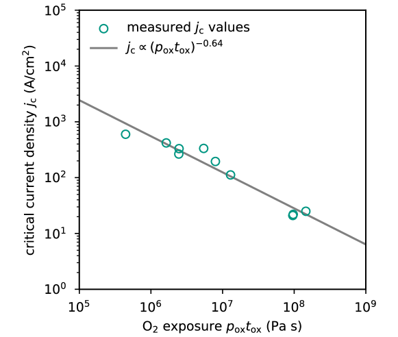
Figure 2 shows the individual fabrication steps for our cross-type Josephson junctions. After trilayer deposition (see figure 2(a)), a positive, high-resolution UV photoresist (AZ MIR 701 29CP supplied by Microchemicals GmbH) is spin-coated on top of the trilayer and patterned as a narrow stripe using direct laser lithography. The width of this stripe defines one of the lateral dimensions of the final Josephson junction (see below). The resulting photoresist mask is used for etching the entire trilayer stack (see figure 2(b)). Both Nb layers are etched by inductively coupled plasma reactive ion etching (ICP-RIE) using SF6 and Ar in a mixing ratio of 2:1 at a constant pressure of as process gas. The rf-power and the ICP power are and , respectively, resulting in an etch rate of . The Al-AlOx layer and the thermal oxide of the Si substrate, respectively, act as etch stop for the ICP-RIE processes. The Al-AlOx layer is wet-chemically etched with an etching solution consisting of phosphoric acid, nitric acid, acetic acid and water that are mixed in a ratio of . As will be shown in section 4, wet-chemical etching of the Al layer is key to guarantee a high junction quality when omitting wet-chemical anodization.
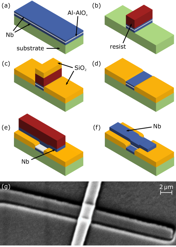
The next step is the deposition of a dielectric insulation layer (see figure 2(c)). The insulation is intended not only to protect the sidewalls of the patterned trilayer stripe, but also to quasi-planarize the layer stack before the deposition of subsequent layers. For deposition, we use the same photoresist mask as for trilayer patterning, i.e. the mask is not removed after the prior etching steps. It is important to note that the photoresist acts as a shadow mask during dc-magnetron sputter deposition, resulting in trenches beside the trilayer stripe. We empirically found that the thickness of the insulation layer at the lowest point of the trenches is only about of the nominally deposited material. For this reason, the thickness of the insulation layer must be at least twice the layer thickness of the Nb base electrode to prevent shorts between the base electrode and subsequent wiring layers. We hence deposit a thick SiO2 layer by rf-magnetron sputtering utilizing a separate HV sputtering system, a gas mixture consisting of Ar and O2 at a constant pressure of as process gas, and an rf-power of . This results in an overall deposition rate of .
After removal of the photoresist mask (see figure 2(d)), a Nb wiring layer with a thickness of is dc-magnetron sputter deposited using a HV sputter system with a base pressure below and a Nb target. The Ar pressure and the dc-power are and , respectively, resulting in a deposition rate of . Prior to the deposition, the surface of the Nb counter electrode (upper Nb layer of the trilayer stripe) is pre-cleaned by Ar ion milling to remove native oxides and hence to ensure a superconducting contact between the counter electrode and the deposited Nb layer. This final layer is patterned by structuring a high-resolution UV photoresist (same as for trilayer patterning) as a narrow stripe that is oriented perpendicular to the embedded trilayer stripe and ICP-RIE for Nb etching. The top Nb layer of the trilayer stack is etched within the same etching cycle to define the final size of the counter electrode (see figure 2(e)). By this, we yield rectangular Josephson tunnel junctions from the overlap of the trilayer and Nb wiring stripes. Finally, the residual Al-AlOx of the trilayer is removed by wet etching to enable later electrical contacts to the Nb base electrode (see figure 2(f)).
It is worth mentioning that the area of our cross-type Josephson junctions is only limited by the resolution of the lithographic tool and not by alignment accuracy. Due to the minimum structure size of our laser lithography tool of , we are able to reliably fabricate cross-type junctions with a nominal area of \qtyproduct1 x 1\micro, but even sub-micrometer-sized junctions are achievable with the help of e.g. DUV steppers or electron beam lithography. Even though such small junctions require higher values of the critical current density to achieve a target value of the critical current, the total junction capacitance is reduced as the intrinsic capacitance linearly decreases with the junction area while the intrinsic capacitance per unit area only logarithmically increases with the critical current density [22, 23]. In addition, the capacitance of cross-type junctions has a negligible parasitic contribution there are no direct wiring overlaps. Besides that, only two lithographic layers are required during the entire fabrication process. The higher values of the critical current density further lower the time taken to fabricate a batch of cross-type junctions as, according to figure 1, the oxidation time for the formation of the tunnel barrier gets significantly shorter assuming a fixed oxidation pressure.
3 Experimental techniques for junction characterization
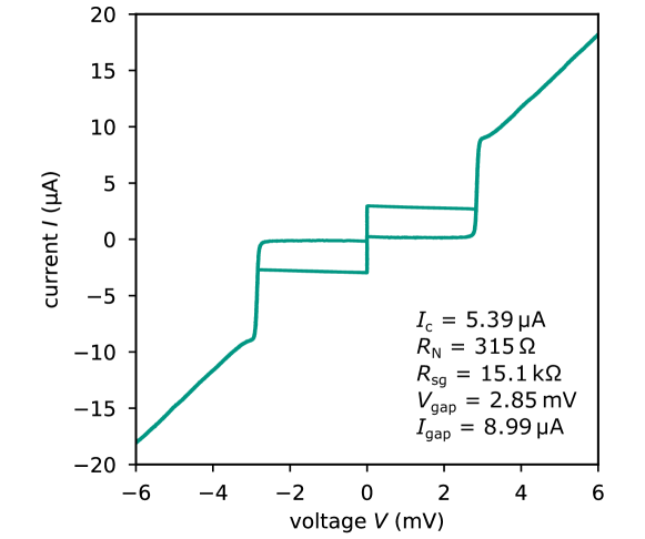
Up to now, we have successfully fabricated more than 15 batches of cross-type junctions with linear dimensions varying between and using our anodization-free fabrication process. The characteristic figures of merit and hence the quality of fabricated junctions as well as their uniformity across an entire wafer were determined by recording the current-voltage () characteristics (see figure 3 as an example) of a sub-sample of each batch at a temperature of in a differential four-wire configuration. The utilized measurement set-up comprises low-pass filters at room and cryogenic temperatures to filter external rf interference signals. The dc bias current is generated by applying a triangular voltage signal with a frequency of to the series connection of all resistors in the input circuit of the set-up. This includes the equivalent resistance of both rf-filters as well as the voltage-dependent resistance of the Josephson junction to be measured. The actual bias current through the junction hence depends on the voltage drop across the junction and is given by
| (1) |
The voltage drop is measured using a battery-powered differential amplifier. To screen the samples from disturbances induced by variations of magnetic background fields, the cryo-probe is equipped with a mu-metal and a superconducting shield made of Nb.
The quality of each Josephson junction is evaluated by means of different figures of merit, among those the critical current , the normal state resistance , the gap voltage , and the subgap resistance . As conventional, the subgap resistance is determined at a voltage value of in the subgap region. From these quantities, the characteristic resistance ratio and the product are calculated. The former is a junction area independent figure of merit to quantify subgap leakage, e.g. due to defects or shorts in the tunnel barrier [24, 25]. The latter is a measure for the strength of Cooper pair tunneling that depends on the profile of the electric potential along the tunnel barrier [26].
The critical current of each Josephson junction was determined by its relation [27] to the gap current , the latter corresponding to the amplitude of the quasiparticles’ tunneling current at the gap voltage, as the switching current at , extracted from -characteristics, is always significantly smaller than the true critical current. The deviation between the switching current and the critical current is caused by thermal noise [28, 29]. The recursion formula
| (2) |
describes the related probability of the Josephson junction to escape from the zero-voltage state at a nominal switching current within the interval when a bias current is injected with a sweep rate . The temperature dependent escape rate
| (3) |
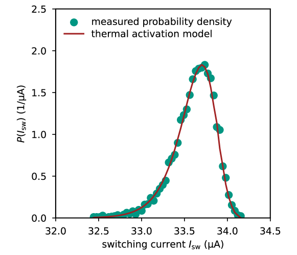
is a function of a temperature and damping dependent thermal prefactor , the oscillation frequency of the Josephson junction with denoting the plasma frequency and the height of the potential barrier [30]. It can be calculated from the measured switching current distribution of a junction to determine its true critical current by using iterative numerical methods [31]. Figure 4 shows as an example of the measured switching current distribution at and a fit according to equations 2 and 3 for one of our cross-type junctions with a critical current of . The dimensionless factor , used to calculate the critical current from the measured gap current, is independent of the junction size and constant for an entire junction batch. It was determined by measuring and evaluating the switching current distribution of some representative junctions from each batch.
In order to investigate the spatial profile of the critical current density along the tunnel barrier, the dependence of the maximum supercurrent through the junction on an external magnetic field was measured [32]. For these measurements, the mu-metal shield of our junction characterization set-up was removed and a Helmholtz coil was attached to the sample holder such that the junction was located in the center of the coil. To analyze the measured data (see, for example, figure 11 in section 4), a model of the distribution of the critical current density was generated and the absolute value of the Fourier transform of this model was compared to the measured data.
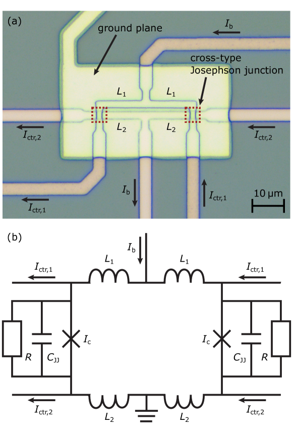
The specific capacitance of our Josephson junctions was determined by observing Shapiro steps in unshunted dc-SQUIDs [33, 34]. For this, two types of symmetric, unshunted dc-SQUIDs based on cross-type junctions were designed and fabricated. Both variants differ by the junction size (see below). Figure 5 shows a micrograph and the corresponding equivalent circuit model of such a current-biased SQUID comprising \qtyproduct2 x 2\micro-sized cross-type Josephson junctions. The SQUID loop with inductance is composed of two sections. The upper section with inductance is patterned from the thick Nb wiring layer. In contrast, the lower section with inductance is formed by the thick lower Nb layer of the trilayer stack. Both sections are connected via the Josephson junctions. Moreover, feedlines for injecting control currents and are connected to both loop sections at the location of the Josephson junctions. A thick Nb ground plane, separated by an insulating SiO2 layer, was patterned on top of all devices to reduce cross-talk between both loop sections [35]. The resulting parasitic capacitance which is connected in parallel to the capacitance of the two Josephson junctions was estimated to be about and corresponds to only of the smallest measured capacitance.
To observe the actual resonance steps in the -characteristic, the maximum supercurrent of a respective sample SQUID was suppressed by applying a control current through one of the feedlines. For with , , and denoting the magnetic flux threading the SQUID loop, the maximum supercurrent is at its minimum. At the same time, the periodicity of the maximum supercurrent modulation with being the current difference between two neighboring minima was used to determine the inductance of the SQUID loop [36]. The value of for our unshunted SQUIDs with \qtyproduct2 x 2\micro-sized junctions was simulated to be using InductEx (numeric simulation software by SUN Magnetics (Pty) Ltd.) and is in perfect agreement with the experimental value of taking into account possible fabrication induced size and alignment variances. We also fabricated devices with \qtyproduct4 x 4\micro-sized cross-type junctions to determine the specific capacitance for junctions with critical current densities . Here, the calculated loop inductance is which is again in good agreement with the experimental value of .
4 Results and discussion
4.1 Sidewall insulation and characteristic resistance ratio
A key factor for the reliable and reproducible fabrication of high-quality cross-type Josephson junctions based on a Nb/Al-AlOx/Nb trilayer stack is a sufficient galvanic isolation between the base electrode of the junction and a subsequent wiring layer to its top electrode. In our process, this insulation is realized by the quasi-planarizing insulation layer with sufficient thickness to compensate for trenching effects and, even more important, the usage of wet-chemical etching for removing the Al-AlOx layer during trilayer etching (see figure 2(b)). During the wet etching process, nitric acid oxidizes the Al surface, while phosphoric acid dissolves the native as well as the continuously formed aluminum oxide. Since niobium, similar to aluminum, oxidizes in nitric acid, but niobium oxide does not dissolve in phosphoric acid [37], an oxide layer of a few nm thickness forms on the exposed sidewalls of the patterned Nb/Al-AlOx stripe and on the surface of the still unstructured lower Nb of the trilayer. This oxide layer serves as a passivation layer. Moreover, compared to plasma induced ion milling no etching residues from redeposited Al atoms [38] appear during wet etching. These residues potentially adhere to the sidewalls of the etched structure forming shorts across the tunnel barrier. Similarly, the passivation layer protects against the formation of shorts originating from potential redeposits during Nb base electrode etching. Overall, the passivation layer formed during wet etching takes on the same task as wet-chemical anodization, however, without the need for a galvanic contact between all patterned trilayer structures.
In order to proof that wet etching of the Al-AlOx layer using our acidic etching solution in fact substitutes the anodization of the sidewalls of the patterned trilayer stack, we prepared two distinct batches of cross-type junctions. The Nb/Al-AlOx/Nb trilayer of both batches was sputtered in the same deposition run by placing both substrates side-by-side on the sample holder in the sputter system. For one batch, the Al-AlOx layer was wet-chemically etched, for the other batch Ar ion milling within the ICP-RIE system was used. For about one half of the Josephson junctions of each batch, the sidewalls were additionally anodized after etching the trilayer stripe.
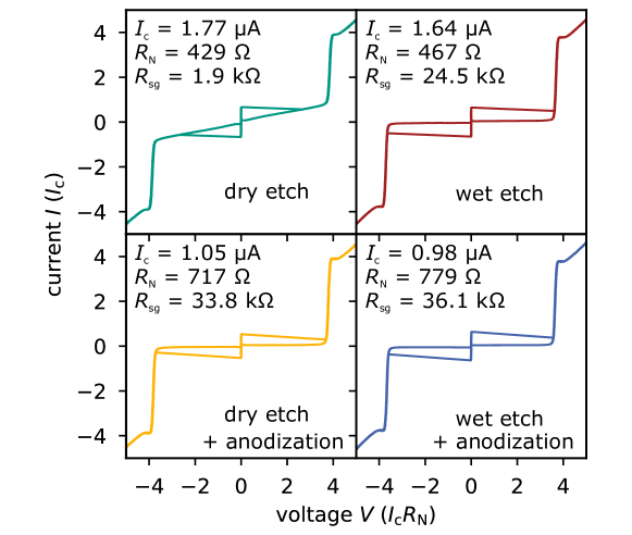
Figure 6 shows current-voltage characteristics of representative cross-type Josephson junctions for each variant. Irrespective of the actual etching technique, the junctions with anodized sidewalls are of high quality which is indicated by very low subgap leakage. Non-anodized junctions for which the Al-AlOx was wet-chemically etched are of the same quality and have low subgap leakage. In contrast, the -characteristics of non-anodized, dry etched cross-type junctions exhibit severe leakage. We attribute this to vertical shorts across the tunnel barrier caused by non-passivated Al and Nb redeposits that are oxidized in case that wet-chemical anodization is subsequently used. We note that the critical current of anodized junctions is about smaller than of non-anodized junctions and attribute this to the reduced junction area due to the thick oxide layer on the sidewalls caused by anodization.
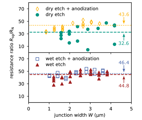
The number of redeposits that potentially lead to shorts across the tunnel barrier and hence the subgap leakage are expected to increase with the junction width . Figure 7 displays the dependence of the characteristic resistance ratio on the width of the quadratic Josephson junctions from the two examined batches and confirms this hypothesis. We observe an increase of spread with increasing junction size for the dry etched junctions with non-anodized sidewalls. Note that the yield of junctions of this variant is only , i.e. about every second junction has very high subgap leakage or shown an ohmic -characteristic. The fact that this large spread is not observed for anodized junctions from the same batch as well as that the yield of all other variants is significantly larger (about 90%) is a clear indication that the leakage originates from the sidewalls and not from the tunnel barrier itself.
The comparison between the non-anodized, wet-chemically etched junctions and the anodized junctions from the same batch as well as the dry etched, anodized junctions (see figure 7) shows that the use of an acidic etching solution for removing the Al-AlOx layer indeed replaces wet-chemical anodization of the sidewalls of cross-type Josephson junctions. These three variants show a small spread of the characteristic resistance ratio. The latter tends to get larger the larger the junction is. We attribute this to edge effects that are not caused by redeposits at the sidewalls. Moreover, a direct comparison of the mean characteristic resistance ratios indicates that wet etched, non-anodized junctions show generally lower subgap leakage than dry etched, anodized specimens. This favors the usage of our fabrication process as compared to processes relying on dry etching the Al-AlOx layer and subsequent wet-chemical anodization.
4.2 Scalability and uniformity of critical current and normal state resistance
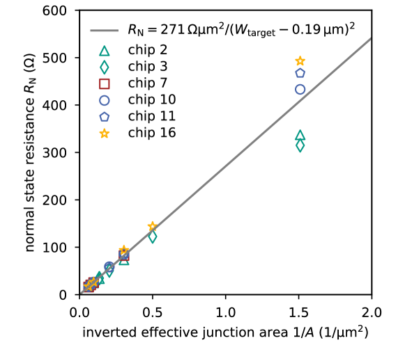
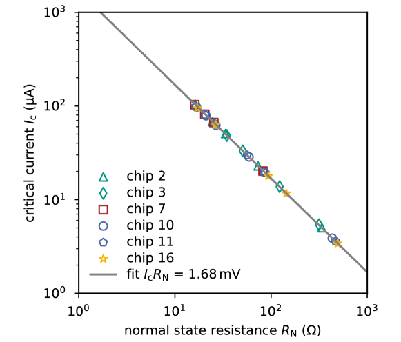
For all batches of Josephson junctions that were produced using our anodization-free fabrication process, we checked for the scalability of the critical current and the normal state resistance with respect to the junction area as well as for the uniformity of these parameters within a batch. Figure 8 and figure 9 show as an example the results for a batch with a critical current density of about . As expected, both, the critical current and the normal state resistance , scale linearly with the effective and the inverse effective junction area, respectively. We note that the effective junction area deviates from the target value as the lateral junction size deviates by a length . We determine the deviation by a linear fit , denoting the normal state resistivity, to the data in figure 8 and find that the size of the cross-type junctions of this example batch is on average only smaller than the target value. We attribute this deviation to size variations in the photoresist masks and to a parasitic lateral material loss during etching. Deviations from the linear fit only occur for the smallest junctions with a target area of , for which a potentially location dependent variation of the junction size has the greatest effect.
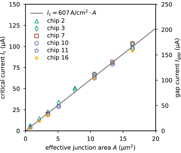
Besides the scalability of the critical current and the normal state resistance, our cross-type junctions also show a high quality that is reflected, for example, by the high average values of the characteristic resistance ratio for small junctions with and for junctions with (compare figure 7) or the value of the gap voltage . For all batches, , i.e. the gap voltage is very close to the value or the energy gap of Nb [39] and the proximity effect due to the Al layer is negligible. We find for the example batch displayed in figure 8 and figure 9 and the values for the gap voltage are only statistically distributed with a standard deviation of . The product (see figure 10) is independent of junction size and is as high as for the example batch discussed here. This observation and the almost size independent resistance ratio (see figure 7) indicate that the performance of Nb/Al-AlOx/Nb Josephson tunnel junctions produced with our cross-type fabrication process is not affected by edge effects caused by the process but rather than by the intrinsic properties of the tunnel barrier that, of course, could be further optimized.
4.3 Profile of the critical current density
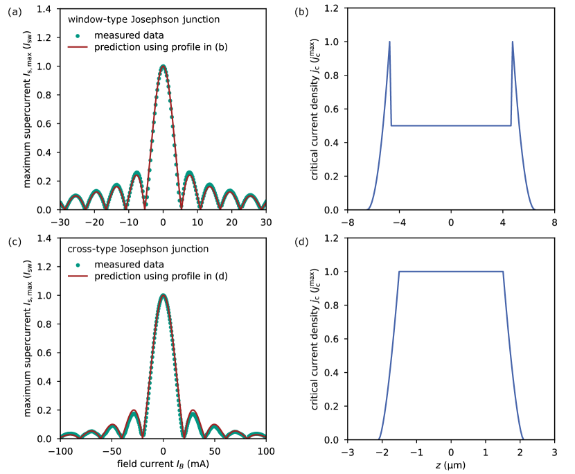
The usage of our fabrication process for cross-type Josephson junctions turns out to positively affect the critical current density profile of the tunnel barrier. This can be seen by a comparison between the critical current density distributions shown in figure 11(b) and figure 11(d). Both profiles were generated as models to describe the measured dependencies of the maximum supercurrent of a \qtyproduct13 x 13\micro window-type and a \qtyproduct4.2 x 4.2\micro cross-type Josephson junction on the current through the Helmholtz coil of our measurement setup (see section 3). The corresponding plots are shown in figure 11(a) and figure 11(c), respectively. The batch of Nb/Al-AlOx/Nb window-type junctions was fabricated separately using an anodization-free process based on the one described in [40] in which the Al-AlOx layer was etched by Ar ion milling. The modeled critical current density profile plotted in figure 11(b) is based on two assumptions: 1.) Due to small damages at the edges of the tunnel barrier during dry etching of the Nb top electrode and the Al-AlOx layer, the flanks of the -profile are not upright but slightly quadratically shaped. 2.) The momentum/energy of the Ar ions during surface cleaning of the top electrode prior to the deposition of the Nb wiring is transferred to the underlying tunnel barrier where it causes damage and thus a reduced critical current density. The area in which this effect occurs is restricted to the size of the window in the insulation layer which is \qtyproduct11 x 11\micro. The measured magnetic field dependence agrees very well with the modeled -profile. The modeled critical current density profile of the cross-type junction shown in figure 11(d) only assumes small damages at the edges of the tunnel barrier during dry etching of the trilayer stack. It clearly exhibits no indentation and yet describes the measured data in figure 11(c) well. Since there is no insulation window on top of the top electrode for a cross-type Josephson junction, the momentum/energy transfer of the Ar ions should be distributed evenly over the entire tunnel barrier, giving rise to a more homogeneous tunnel barrier.
4.4 Capacitance measurements
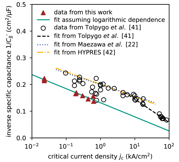
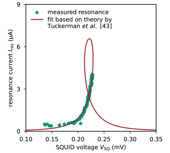
We measured the capacitance of several cross-type Josephson junctions taken from batches with different critical current densities using unshunted dc-SQUIDs as described in section 3. As the parasitic capacitance is expected to be negligible due to the missing overlap of wiring layers, the measured values should resemble the intrinsic capacitance related to the tunnel barrier. Figure 12 summarizes the result of our measurements and shows the dependence of the inverse junction capacitance per junction area on the critical current density for each measured SQUID. We note that the specific capacitance is derived from the measured capacitance value as well as the effective junction area that is determined from fitting the dependence of the normal state resistance on the junction area (see section 4.2). Moreover, figure 13 shows an example of a recorded Shapiro step of a current-biased SQUID with an experimentally determined loop inductance of and a critical current of of the Josephson junction. The resonance voltage for deriving the junction capacitance
| (4) |
was determined by fitting the expected shape of the resonance curve to the actual data [43]. The value of the damping parameter required for performing this fit was extracted from its relation to the current ratio [44]. For the resonance curve shown in figure 13, . The amplitude of the measured resonance step does not reach the theoretically expected value due to thermal suppression at .
The solid line in figure 12 represent a fit to the data assuming a logarithmic dependence of the specific capacitance on the critical current density [22, 23]. We find
| (5) |
For comparison, we also display the data and derived functional dependencies of the specific capacitance published in [41] and the references therein. We see that in a critical current density range between approximately and the slope of the functional dependence of our cross-type Josephson junctions is similar to those published by other research groups [22, 42]. Nevertheless, the offset is slightly higher which might be related to different crystal structures of the aluminum oxide barrier.
5 Conclusion
We have developed an anodization-free fabrication process for Nb/Al-AlOx/Nb cross-type junctions. Our process requires only a small number of fabrication steps and is intrinsically compatible with wafer-scale fabrication. Fabricated junctions are of very high-quality as indicated by the measured values for the subgap to normal state resistance ratio and the product. Compared to other junction types manufactured under the same technical conditions, our cross-type Josephson junctions show not only a significantly reduced specific capacitance but also an almost rectangular critical current density profile. Our process hence enables the usage of low capacitance Josephson junctions for superconducting electronic devices such as ultra-low noise dc-SQUIDs, microwave SQUID multiplexers based on non-hysteretic rf-SQUIDs, and RFSQ circuits.
Acknowledgments
We would like to thank A Reifenberger, O Kieler and T Wolf for support during device fabrication and characterization. Moreover, we thank A Ferring, C Jakob, M Schmelz, and R Stolz for fruitful discussions. F Bauer acknowledges former financial support by the Helmholtz Graduate School for Hadron and Ion Research (HGS-HIRe of FAIR). The research leading to these results has also received funding from the European Union’s Horizon 2020 Research and Innovation Programme, under Grant Agreement No. 824109.
Data Availability Statement
The data that support the findings of this study are available from the corresponding author upon reasonable request.
References
References
- [1] Clarke J and Wilhelm F K 2008 Nature 453 1031–42 URL https://doi.org/10.1038/nature07128
- [2] Fagaly R L 2006 Review of Scientific Instruments 77 URL https://doi.org/10.1063/1.2354545
- [3] Yohannes D T, Hunt R T, Vivalda J A, Amparo D, Cohen A, Vernik I V and Kirichenko A F 2015 IEEE Transactions on Applied Superconductivity 25(3) 1100405 URL https://doi.org/10.1109/TASC.2014.2365562
- [4] Kunert J, Ijsselsteijn R, Il’ichev E, Brandel O, Oelsner G, Anders S, Schultze V, Stolz R and Meyer H G 2017 Low Temperature Physics 43(7) 785 URL https://doi.org/10.1063/1.4995626
- [5] Hamilton C A 2000 Review of Scientific Instruments 71 URL https://doi.org/10.1063/1.1289507
- [6] Blüthner K, Götz M, Krech W, Mühlig H, Wagner T, Fuchs H J, Bluthner K, Gotz M, Muhlig H, Schelle D, Fritzsch L, Nachtmann B and Nowack A 1996 Journal de Physique IV Proceedings 111(C3) 3–163 URL http://dx.doi.org/10.1051/jp4:1996325
- [7] Dolata R, Scherer H, Zorin A B and Niemeyer J 2005 Journal of Applied Physics 97(5) URL https://doi.org/10.1063/1.1855399
- [8] Bhat A, Meng X, Whiteley S, Jeffery M and Duzer T V 1999 IEEE Transactions on Applied Superconductivity 9(2) 3232–3235 URL https://doi.org/10.1109/77.783717
- [9] Aumentado J 2020 IEEE Microwave Magazine 21(8) 45–59 URL https://doi.org/10.1109/MMM.2020.2993476
- [10] Rothermel H, Gundlach K H and Voss M 1994 Le Journal de Physique IV 04(C6) 267 URL https://doi.org/10.1051/jp4:1994643
- [11] Westig M P, Justen M, Jacobs K, Stutzki J, Schultz M, Schomacker F and Honingh N 2012 Journal of Applied Physics 112(9) 093919 URL https://doi.org/10.1063/1.4764324
- [12] Clarke J and Braginski A I (eds) 2004 The SQUID Handbook: Vol. 1 Fundamentals and Technology of SQUIDs and SQUID Systems (Wiley-VCH Verlag GmbH & Co. KGaA) ISBN 3527402292
- [13] Gurvitch M, Washington M A and Huggins H A 1983 Applied Physics Letters 42(5) 472 URL http://aip.scitation.org/doi/10.1063/1.93974
- [14] Dolata R, Weimann T, Scherer H J and Niemeyer J 1999 IEEE Transactions on Applied Superconductivity 9(2) 3255 URL https://doi.org/10.1109/77.783723
- [15] Ketchen M B, Pearson D, Kleinsasser A W, Hu C K, Smyth M, Logan J, Stawiasz K, Baran E, Jaso M, Ross T, Petrillo K, Manny M, Basavaiah S, Brodsky S, Kaplan S B, Gallagher W J and Bhushan M 1991 Applied Physics Letters 59(20) 2609–2611 URL https://doi.org/10.1063/1.106405
- [16] Bao Z, Bhushan M, Han S and Lukens J E 1995 IEEE Transactions on Applied Superconductivity 5(2) 2731–2734 URL https://doi.org/10.1109/77.403155
- [17] Watanabe M, Nakamura Y and Tsai J S 2004 Applied Physics Letters 84(3) 410–412 URL https://doi.org/10.1063/1.1640798
- [18] Harada Y, Haviland D B, Delsing P, Chen C D and Claeson T 1994 Applied Physics Letters 65(5) 636–638 URL https://doi.org/10.1063/1.112255
- [19] Dang H and Radparvar M 1991 IEEE Transactions on Magnetics 27(2) 3157 URL https://doi.org/10.1109/20.133881
- [20] Anders S, Schmelz M, Fritzsch L, Stolz R, Zakosarenko V, Schönau T and Meyer H G 2009 Superconductor Science and Technology 22(6) 064012 URL http://dx.doi.org/10.1088/0953-2048/22/6/064012
- [21] Kaiser C, Meckbach J M, Ilin K S, Lisenfeld J, Schäfer R, Ustinov A V and Siegel M 2011 Superconductor Science and Technology 24 URL http://dx.doi.org/10.1088/0953-2048/24/3/035005
- [22] Maezawa M, Aoyagi M, Nakagawa H, Kurosawa I, Takada S and Tuckerman A 1995 Applied Physics Letters 66(16) 2134 URL https://doi.org/10.1063/1.113927
- [23] Tolpygo S K, Yohannes D, Hunt R T, Vivalda J A, Donnelly D, Amparo D and Kirichenko A F 2007 IEEE Transactions on Applied Superconductivity 17(2) 946 URL https://doi.org/10.1109/TASC.2007.898571
- [24] Kuroda K and Yuda M 1988 Journal of Applied Physics 63(7) 2352 URL https://doi.org/10.1063/1.341051
- [25] Du J, Charles A D M, Petersson K D and Preston E W 2007 Superconductor Science and Technology 20(11) S350 URL https://doi.org/10.1088/0953-2048/20/11/S10
- [26] Likharev K K 1986 Dynamics of Josephson Junctions and Circuits (Taylor & Francis) ISBN 9782881240423
- [27] Likharev K K 1979 Reviews of Modern Physics 51(1) 101 URL https://doi.org/10.1103/RevModPhys.51.101
- [28] Fulton T A and Dunkleberger L N 1974 Physical Review B 9(11) 4760 URL https://doi.org/10.1103/PhysRevB.9.4760
- [29] Danchi W C, Hansen J B, Octavio M, Habbal F and Tinkham M 1984 Physical Review B 30 2503–2516 URL https://doi.org/10.1103/PhysRevB.30.2503
- [30] Wallraff A, Lukashenko A, Coqui C, Kemp A, Duty T and Ustinov A V 2003 Review of Scientific Instruments 74(8) 3740 URL https://doi.org/10.1063/1.1588752
- [31] Castellano M G, Leoni R, Torrioli G, Chiarello F, Cosmelli C, Costantini A, Diambrini-Palazzi G, Carelli P, Cristiano R and Frunzio L 1996 Journal of Applied Physics 80(5) 2922 URL https://doi.org/10.1063/1.363147
- [32] Barone A and Paternò G 1982 Physics and Applications of the Josephson Effect (John Wiley & Sons, Inc.) ISBN 9783527602780
- [33] Guéret P 1979 Applied Physics Letters 35(11) 889 URL https://doi.org/10.1063/1.90995
- [34] Magerlein J H 1981 IEEE Transactions on Magnetics MAG-17(1) 286 URL https://doi.org/10.1109/TMAG.1981.1060968
- [35] Williams T 2017 EMC for Product Designers 5th ed (Newnes) ISBN 978-0-08-101016-7
- [36] Henkels W H 1978 Applied Physics Letters 32(12) 829 URL https://doi.org/10.1063/1.89940
- [37] Koch C and Rinke T J 2017 Photolithography: Basics of Microstructuring 1st ed (MicroChemicals GmbH) ISBN 978-3-9818782-1-9
- [38] Lehmann H W, Krausbauer L and Widmer R 1977 Journal of Vacuum Science and Technology 14(1) 281 URL https://doi.org/10.1116/1.569140
- [39] Carbotte J P 1990 Reviews of Modern Physics 62(4) 1027–1157 URL https://doi.org/10.1103/RevModPhys.62.1027
- [40] Kempf S, Ferring A, Fleischmann A, Gastaldo L and Enss C 2013 Superconductor Science and Technology 26(6) 065012 URL http://dx.doi.org/10.1088/0953-2048/26/6/065012
- [41] Tolpygo S K, Bolkhovsky V, Zarr S, Weir T J, Wynn A, Day A L, Johnson L M and Gouker M A 2017 IEEE Transactions on Applied Superconductivity 27(4) 1100815 URL https://doi.org/10.1109/TASC.2017.2667403
- [42] Hypres niobium integrated circuit fabrication, process #03-10-45, design rules, revision #25, 12/12/2012 URL https://www.hypres.com/wp-content/uploads/2010/11/DesignRules-4.pdf
- [43] Tuckerman D B and Magerlein J H 1980 Applied Physics Letters 37(2) 241 URL https://doi.org/10.1063/1.91839
- [44] Paternò G, Cucolo A M and Modestino G 1985 Journal of Applied Physics 57(5) 1680 URL https://doi.org/10.1063/1.334437