Fault-tolerant Quantum Error Correction Using a Linear Array of Emitters
Abstract
We propose a fault-tolerant quantum error correction architecture consisting of a linear array of emitters and delay lines. In our scheme, a resource state for fault-tolerant quantum computation is generated by letting the emitters interact with a stream of photons and their neighboring emitters. In the absence of delay line errors, our schemes have thresholds ranging between and against the standard circuit-level depolarizing error model. Depending on the number of emitters , we study the effect of delay line errors in two regimes: when is a small constant of order unity and when scales with the code distance. Between these two regimes, the logical error rate steadily decreases as increases, from an exponential decay in to an exponential decay in . We also carry out a detailed study of the break-even point and the fault-tolerance overhead. These studies suggest that the multi-emitter architecture, using the state-of-the-art delay lines, can be used to demonstrate error suppression, assuming other sources of errors are sufficiently small.
I Introduction
One of the fundamental discoveries in quantum computation is the theory of fault-tolerant quantum computation Gottesman (1998a, b, 2009); Kitaev (2003); Aharonov and Ben-Or (2008); Knill et al. (1998). While realistic quantum computers are noisy, if their noise rate is below the fault-tolerance threshold, one can simulate the behavior of a noiseless quantum computer arbitrarily well using a noisy quantum computer.
Recently, rapid progress in quantum computing technology led to an explosion of works on fault-tolerant quantum computing architectures Barends et al. (2014); Arute et al. (2019); Harty et al. (2014); Ballance et al. (2016); Monroe and Kim (2013); Madsen et al. (2022); Levine et al. (2019); Norcia et al. (2018); Saskin et al. (2019); Covey et al. (2019). These studies aim to develop protocols tailored to specific hardwares, with the goal of maximizing the efficiency of the underlying error correction protocols. One of the most well-studied architecture is the surface-code based architecture, which are well-suited for planar array of superconducting qubits Fowler et al. (2012). Recent advances led to novel architectures suitable for implementing quantum low-density parity check codes Tremblay et al. (2022); Delfosse et al. (2021); Strikis and Berent (2023); Xu et al. (2023). These theoretical advances were also accompanied by recent experimental milestones that demonstrate quantum error correction Acharya et al. (2022); Ryan-Anderson et al. (2021, 2022); Bluvstein et al. (2023).
However, near-term quantum computers are still not powerful enough to carry out commercially useful quantum computations. A commonly cited commercial application of quantum computation is the study of challenging molecules such as FeMoCo Reiher et al. (2016). However, in spite of the progress made in quantum algorithms, the number of -gates — the most expensive fault-tolerant gate due to the costly magic state distillation — is still estimated to be between and , with the number of logical qubits estimated to be at least Lee et al. (2020); von Burg et al. (2020).
Manufacturing and controlling such large number of qubits can pose a significant challenge. However, it is possible to mitigate this challenge by exploiting the unique physics provided by certain platforms. One such approach is to use a single-photon emitter such as quantum dot. With photons, a promising approach is to build a cluster state, which is a resource state for measurement-based quantum computation (MBQC) Raussendorf and Briegel (2001); Raussendorf et al. (2003) as an avenue for doing quantum computation quite distinct from those based on unitary circuits. Preparation of cluster state using photons is a well-studied subject. Many protocols have been studied both theoretically and experimentally Nielsen (2004); Walther et al. (2005); Lindner and Rudolph (2009); Economou et al. (2010); Yokoyama et al. (2013); Yoshikawa et al. (2016); Schwartz et al. (2016); Pichler et al. (2017); Larsen et al. (2019); Asavanant et al. (2019); Wan et al. (2021); Shi and Waks (2021); Ferreira et al. (2022); Roh et al. (2023); Bartolucci et al. (2021); Bombin et al. (2021); Bourassa et al. (2021); Tzitrin et al. (2021).
For instance, it is well-known that an emitter can be used to create a one-dimensional cluster state Lindner and Rudolph (2009). By using a single delay line, a single emitter can prepare a two-dimensional cluster state Pichler et al. (2017); Ferreira et al. (2022), which can be used for universal measurement-based quantum computation Raussendorf et al. (2003).
With an additional delay line, one can even prepare a three-dimensional cluster state Wan et al. (2021), which is a resource state for universal fault-tolerant quantum computation Raussendorf et al. (2005, 2006, 2007); Roh et al. (2023). In this scheme, all that is required for building a fault-tolerant logical qubit is a single emitter, two delay lines, and a single-photon detector. Compared to the alternatives which would require controlling hundreds if not thousands of physical qubits, the demand on the number of experimental components is more modest.
However, there is an important caveat. The error rate one needs to demonstrate error suppression puts a challenging demand on the quality of the delay line. Assuming that the error rate per unit length in the delay line is , it was shown in Ref. Wan et al. (2021) that the logical error rate decays exponentially with , provided that the other error rates (e.g., two-qubit gates between the emitter and the photon) smaller than a threshold. Unfortunately, assuming the circuit-level noise is a depolarizing noise of strength of , the existing state-of-the-art (loss) error rates reported in the commercial delay lines Tamura et al. (2018) were below the break-even point Wan et al. (2021). More precisely, if one were to use such a delay line, logical error rate after error correction is expected to be strictly higher than the circuit-level error. As such, while the approach of Ref. Wan et al. (2021) was conceptually appealing, it did not seem practical considering the current experimental capabilities.
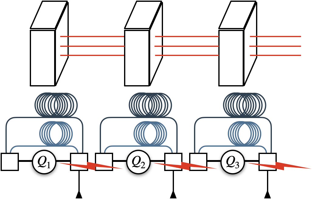
The main purpose of this paper is to study a generalization of the scheme in Ref. Wan et al. (2021) that can mitigate this issue. Our scheme involves emitters that are arranged on a linear array. What we envision is a scheme similar to the one proposed in Ref. Wan et al. (2021), but including extra emitters that can interact with their neighboring emitters. A schematic description of our approach is shown in Figure 1. We note that such a gate can be applied between a pair of quantum dots, for instance Xue et al. (2021); Noiri et al. (2022); Mills et al. (2022); Madzik et al. (2022); Philips et al. (2022).
Generally speaking, as the number of emitters increase, the performance of our scheme (quantified in terms of the lowest logical error rate one can achieve) improves. We discuss these improvements on three fronts. First, if the number of emitters is a constant of order unity (e.g., 2 or 3), the logical error rate decays exponentially with . While this may seem like a modest improvement over the scaling in Ref. Wan et al. (2021), we emphasize that the logical error rate decays exponentially with these numbers. Therefore, increasing by a factor of few can lead to a factor of few orders of magnitude change in the logical error rate. We observe this phenomena in our numerical studies.
Second, if the number of emitters is large, we obtain a more favorable scaling form for the logical error rate. If is linear in the code distance , we find the logical error rate to decay exponentially with (instead of ), where . Between this regime and the regime in which , the logical error rate steadily improves as increases.
Our improvement stems from the fact that the time each photon experiences in the delay line can be reduced as we increase the number of emitters. Thus by increasing the number of emitters, one effectively reduces the amount of error each photon is experiencing in the delay line. This explains why, as we increase the number of emitters, the logical error rate improves. This suggests that increasing the number of emitters is generally favorable, provided that the two-qubit error rates between the neighboring emitters are sufficiently low.
Experimentally, while two-qubit gate fidelities exceeding 99% have been demonstrated in a small number of quantum dots Xue et al. (2021); Noiri et al. (2022); Mills et al. (2022); Madzik et al. (2022), scaling this to a larger number may lead to a lower fidelity. (However, see Ref. Philips et al. (2022) for the recent advance in scaling the system to up to six quantum dots.) Therefore, a potential concern for our scheme is the practical challenge in scaling the system whilst ensuring high two-qubit gate fidelities.
However, we show in this paper that the two-qubit error rate one can tolerate is significantly higher than what one might naively expect. We consider an anisotropic error model in which the ratio between the two-qubit error rate between the emitters and the other gates can be varied. When , we find that the thresholds of our schemes remain practically unchanged even if we assume that the two-qubit error rate between the emitters is almost ten times larger than the other error rates. When is large, the thresholds of our schemes do depend on the error ratio, though still in the range of , similar to the thresholds of the single-emitter protocols Wan et al. (2021). Thus our scheme is tolerant against such experimentally motivated noise models.
The rest of the paper is structured as follows. In Section II, we provide an executive summary of a cluster state preparation protocol which involves a single emitter and two delay lines. This is similar to the one proposed in Ref. Wan et al. (2021), but modified in a way that is suitable for the generalization presented in Section III. In Section III, we propose several cluster state preparation protocols using multiple emitters and delay lines. In Section IV.1, we study the threshold of our scheme by varying the number of emitters over several different error models, in the absence of delay line error. We find the threshold to remain largely intact, independent of the number of emitters, even if the gates between the emitters are far noisier than the other gates. In Section IV.2, we extend the analysis in Section IV.1 to the setup in which the delay line error is present. In Section IV.3, we addressed the improvement of a multi-emitter protocol in comparison to a single-emitter protocol. In Section V, we conclude with a discussion. In particular, we focus on the prospect of achieving error suppression using realistic experimental parameters, using the multi-emitter architecture we propose.
II Single emitter protocols
In this Section, we provide an executive summary of a protocol for preparing a three-dimensional (3D) cluster state using a single emitter. While the main body of our work follows that of Ref. Wan et al. (2021), we also make some changes that are suitable for our generalization to the multi-emitter protocols in Section III.
Physically, the emitter can be an atom or a quantum dot. However, our exposition will simply view them as a qubit, interacting with photons, which can be viewed as another qubit. To differentiate the two, we shall refer to the emitter as the ancilla qubit and the photons as data qubits. From this perspective, the operations enacted on the emitter and the photons are simply the oft-used gates such as controlled- (), controlled-NOT (), and Hadamard. (Note, however, that the entangling gate is only applied between the ancilla and a data qubit, not between data qubits.) For the details on the experimental implementation, see Ref. Wan et al. (2021).
The main purpose of using these gates is to ultimately prepare some cluster states, also known as graph states. This state is defined in terms of a graph . Here is a set of vertices and is a set of (undirected) edges. We will represent the edge between vertices as . Then the cluster state is defined as
| (1) |
where is the gate on the edge. Note that the vertices in the graph only involve the data qubits. The ancilla qubit only assists in creating the target cluster state ; it is not part of the qubits that constitute . The cluster state can be described also in terms of the stabilizers. The canonical generating set of the stabilizer group is , where we denoted Pauli- and Pauli- on vertex as and , respectively.
II.1 Cluster state construction from a single emitter
Here we explain a general approach to prepare a cluster state, following the discussion in Ref. Wan et al. (2021). A conventional approach is to prepare all the qubits in the state and apply gate over every edge Raussendorf and Briegel (2001); Raussendorf et al. (2003). However, in our physical setup we cannot apply such gates directly because it is difficult to directly apply an entangling gate between two photons.
One of the key technical observations in Wan et al. (2021) is that such operation can be mediated through an ancilla qubit. Here is the key identity:
| (2) |
where is the ancilla qubit and is the gate acting on qubits and . The protocols we describe below are based on the repeated use of Eq. (2).
To that end, define a sequence of subgraphs and a quasi-subgraph of the graph as follows:
| (3) |
where is a subset of data qubits whose elements are labeled by a non-negative integer, and is the set of edges among the data qubits in . The quasi-subgraph contains, in addition to the vertices and edges in , a vertex corresponding to the ancilla qubit and an additional edge between and the -th qubit.
We can repeatedly apply Eq. (2). Without loss of generality, the cluster state obtained at the -th step is related to the one at the -th step as follows Wan et al. (2021)
| (4) |
While the operation can be easily applied in our setup, the gate is not. This difficulty can be circumvented by using another key identity Wan et al. (2021):
| (5) |
where is a gate with the ancilla as the control qubit and is an arbitrary state of . With this identity, the operations in Eq. (4) be realized entirely in terms of the Hadamard on , and gates between (as the control) and a data qubit. Thus we can sequentially build up the cluster state, arriving at . (Here is the number of vertices.)
To that end, we introduce a unitary :
| (6) |
and rewrite in Eq. (4) as
| (7) |
The state is obtained by applying through on the initial product state . At the very end, we apply to disentangle the ancilla from the data qubit and obtain :
| (8) |
This completes the generation of the desired cluster state .
II.2 Protocols
There were several protocols proposed in Ref. Wan et al. (2021) for cluster state preparation. We found that some of those are readily generalized to the multi-emitter setup whereas some are not. We introduce two protocols — Protocol S1 and Protocol S2— that are easily adaptable to the multi-emitter case.111For the readers familiar with Ref. Wan et al. (2021), we remark that our Protocol S1 is in fact Algorithm 2 of Ref. Wan et al. (2021). Also, Protocol S2 is a slight variant of Protocol B in Ref. Wan et al. (2021); here we apply prior to measuring in the Z-basis whereas in Ref. Wan et al. (2021), they apply after the measurement, specifically when the measurement outcome is . (Here the Roman letter S stands for the single emitter.) The main difference between the two protocols is that Protocol S1 is purely unitary whereas Protocol S2 involves measurements and re-initialization of .
We remark that the conditional statement in the protocols are included to minimize redundant operations, thereby avoiding extra unnecessary errors. More precisely, if belongs to the graph , in Eq. (6) involves the application of twice. This is because the qubit is linked to the ancilla qubit in the quasi-subgraph . Consequently, executing the optimized version of (lines 4-8 in Protocol S1) results in fewer errors. In Protocol S2, lines 4-9 correspond to the optimized for that protocol.
At first, one might worry that these protocols involve interaction of the ancilla qubit with an extensive number of data qubits. This can potentially lead to a single error on the ancilla qubit propagating to an extensive number of qubits. However, a remarkable fact first discovered in Ref. Wan et al. (2021) is that their protocols do not lead to such adverse propagation of errors. A similar analysis can be carried out for our protocols. Also in our protocols one can find that the circuit-level one- or two-qubit errors propagate to, up to stabilizers, errors of constant weight.
II.3 Fault-tolerant error correction
Once a (noisy) 3D cluster state is prepared, one can measure all the qubits in the -basis. These measurement outcomes can be then fed into a decoder, which returns a correction. By studying whether the error and the correction form a logical operator or not, one can decide whether a logical error occurred or not Dennis et al. (2002); Raussendorf et al. (2005, 2006, 2007). We carried out such a numerical simulation using Protocols S1 and S2, the result of which is presented below. (We assumed periodic boundary condition for both Protocols S1 and S2.) Throughout this paper we used the minimum-weight perfect matching (MWPM) decoder, employing the open source code PyMatching Higgott and Gidney (2022) and Stim Gidney (2021).
II.3.1 Circuit-level noise
We first study the performance of Protocol S1 and S2 under the standard circuit-level depolarizing noise. This is the standard model in which a single- and two-qubit depolarizing noise is applied after a single- and two-qubit gate is applied:
| (9) | ||||
where , , , and are the identity and the three Pauli gates acting on the vertex . Here is the single-qubit depolarizing channel of strength applied to qubit and is the two-qubit depolarizing channel over qubit and .
Against this noise model, we estimated the logical error rate for a 3D cluster state of size , where is even to satisfy periodic boundary condition. We averaged over realizations for each choice of and . We estimate the logical error rate by fitting the data to a quadratic scaling ansatz
| (10) |
where and are determined by fitting the data.
The results of these simulations are shown in Figure 3. The threshold values of and were obtained for Protocols S1 and S2, respectively. We remark that the threshold value of for Protocol S2 is the same as that of Protocol B in the Ref. Wan et al. (2021), as expected. However, the logical error rates of Protocol S2 we obtain are higher than those obtained in Wan et al. (2021). This is likely due to the different boundary conditions employed in our calculations. (We used the periodic boundary condition whereas Ref. Wan et al. (2021) used an open boundary condition.)

II.3.2 Delay line error
The study in Section II.3.1 excludes an important source of error. Recall that the data qubits are photons, which at times propagate through a delay line. Each photon experiences an error for each unit of length they travel. We include the effect of such delay line error, following the discussion in Ref. Wan et al. (2021).
The error associated with each delay line — from the emission of the data qubit into the delay line to the eventual measurement — is proportional to the time the photon spends in the delay line. This is equal to the time it takes to apply , which will constitute a convenient unit of time. We assume that each operation consumes an equal amount of time. Throughout this paper, we will assume that there is a fixed error rate associated with this unit time, denoted as with an appropriate subscript, as we describe below.
There are two primary sources of errors in the delay line: dephasing and (heralded) loss error. Dephasing error is a stochastic application Pauli- errors on the data qubit with error rate :
| (11) |
The errors are repeatedly applied for every unit of time to every data qubit traveling in the delay line.
For the loss error, instead of applying the loss error for every unit of time, we consider a phenomenological noise model in which a loss error proportional to the total length of the delay line is applied at the very end of the protocol. This time is proportional to in the leading order, and as such, the error model can be described as follows:
| (12) |
(We will justify this phenomenological noise model further later in this Section, while discussing Table 1.)
Under the error models in Eq. (11) and (12), there cannot be a threshold because the error rate increases with . The optimal choice of is proportional to (with appropriate subscripts, depending on the error model) Wan et al. (2021); Shapourian and Shabani (2022), whose precise value can be obtained by increasing for a fixed value of until logical error rate starts to increase.
For the readers’ convenience, we briefly review the heuristic reason behind this scaling. While the strength of the circuit-level noise remains as a constant, independent of the system size, the delay line error on each qubit scales with . If the circuit-level error is smaller than the threshold, there is a constant amount of error budget for the delay line such that, if we are below this budget, the total amount of error is still below the threshold, ensuring error suppression. This means that, insofar as is smaller than some constant, the logical error rate is exponentially small in . The best possible choice of such is clearly proportional to . Consequently, the optimal logical error rate (denoted as ) becomes Shapourian and Shabani (2022):
| (13) |
for some constants .
Now let us discuss the simulation results for Protocols S1 and S2 under these error models. For the dephasing error [Eq. (11)], the circuit-level noise discussed in Section II.3.1 remains the same. For the loss error [Eq. (12)], we have removed the circuit-level noise and used the decoding algorithm in Ref. Barrett and Stace (2010). (As we said already, though this noise model may seem overly simplistic, we will justify this error model further.)
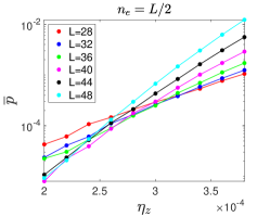
For the dephasing error model [Eq. (11)], we averaged over samples for each choice of , fixing the circuit-level noise as . For both Protocols S1 and S2, Eq. (13) describes our data points well, as expected; see the bottom left plots of Figure 4. The same conclusion applies to the loss error model [Eq. (12)] as well; see the rightmost figures in Figure 4.
It is interesting to see what kind of error rate () is needed to achieve a desired logical error rate . We have listed these values in Table 1 (top) for the target logical error rate of . The same set of values was obtained in Ref. Wan et al. (2021) using Protocol S2 and we listed them in Table 1 (bottom) to compare against ours.
Let us first compare the result obtained for the dephasing error model. One can see that, in order to achieve the same logical error rate, our scheme requires a lower dephasing error than that of Ref. Wan et al. (2021). We expect this discrepancy to be stemming from the different choice of boundary conditions; we used periodic boundary condition whereas the in Ref. Wan et al. (2021) they used open boundary condition. This suggests that it will be more advantageous employ the open boundary condition.
Now we discuss the results obtained from the loss error model. As one can see in Table 1, in order to achieve the same logical error rate, the physical loss error rate needed in our scheme is lower compared to that of Ref. Wan et al. (2021). Therefore, our estimate on the requisite loss error rate to achieve the target logical error rate can be viewed as a conservative lower bound on what is actually needed. The discrepancy between our result and the result in Ref. Wan et al. (2021) is due to the choice of different boundary conditions and loss error model.
Recall that the scheme in Ref. Wan et al. (2021), even applied to the state-of-the-art loss error rate delay line Tamura et al. (2018), does not yield any error suppression. Because the scheme discussed in this Section performs worse than that of Ref. Wan et al. (2021), this scheme will also not yield any error suppression. However, the schemes discussed in Section III will be tantalizingly close to achieving error suppression, assuming the delay line error is equal to the one reported in Ref. Tamura et al. (2018); see Section IV. Accounting for the improvement in logical error rate one can have upon employing the open boundary condition (as in Ref. Wan et al. (2021)), we anticipate error suppression to be well within the reach by using the multi-emitter approach delineated in Section III, applied to the periodic boundary condition; see Section V.
III Multi-emitter protocols
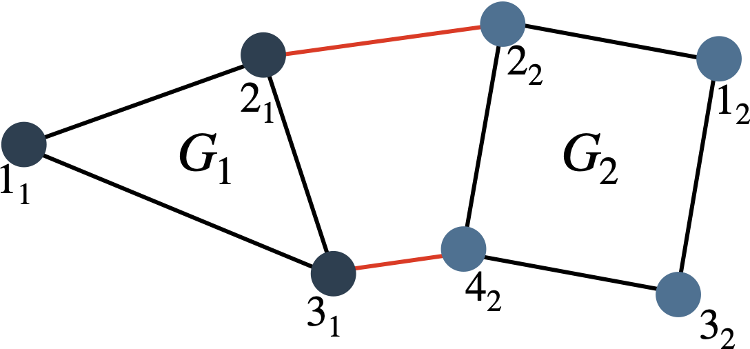
In this Section, we introduce a generalization of the protocols in Section II to the one that involves multiple emitters. A schematic description of our setup is shown in Figure 1.
At a high level, our approach can be explained as follows. Instead of using the single emitter to build up the entire cluster state, we distribute this task to multiple emitters and delay lines. Each emitter is connected to two delay lines as before, and the emitters form a linear array, as shown in Figure 1. Each emitter is responsible for building up a thin “slab” of 3D cluster state, whose thickness is for the cluster state of size , where is the number of emitters.
Of course, as it stands the state being created will be simply a set of disconnected 3D cluster states on different slabs. In order to build an isotropic 3D cluster state of size , we need to further generate entanglement between these slabs. Happily, such entanglement can be generated by a simple modification of the single-emitter protocol [Section II], by intermittently applying an entangling gate between the neighboring emitters without having to entangle the data qubits belonging to different slabs.
We will first go through a simple example illustrating this idea in Section III.1. The general procedure shall be explained in Section III.2.
III.1 Two emitters: an example
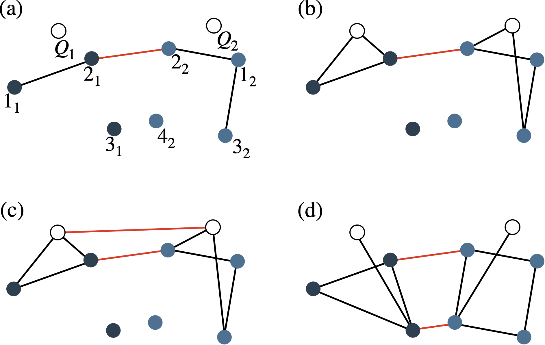
Before we describe our protocol in its full generality, let us start with an instructive example, focusing on the part of the protocol that differs the most from the single-emitter protocol [Section II]. Without loss of generality, suppose our goal is to prepare a cluster state associated with a graph . Assume that this graph can be partitioned into two subgraphs and so that (i) and (ii) and are edges inherited from and , respectively. Note that there are additional edges connecting the vertices across and ; we will denote the set of these edges as .
By running the single-emitter protocol for and concurrently, it is straightforward to create a tensor product of cluster states, each associated with and . However, we also need to generate entanglement associated with the edges in . How can we do that?
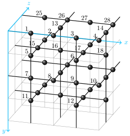
Consider an example of a graph shown in Figure 5. If we grow the cluster state associated with the graph by adding one vertex and the edges connected to that vertex at a time following the numbering convention, there will be two steps in which we would need to generate an entanglement associated with edges in : and . (Here the subscripts and represent the vertices in and , respectively.) Because the underlying procedure is similar, we will focus on the latter. Suppose we have already created a cluster state associated with all the vertices in Fig. 5 except and . When we add and to the existing cluster, we need to add new edges, some of which are in and the rest in .
If we were to only add the edges in , we can simply follow the single-emitter protocol [Section II]. For each subgraph and , we can introduce an ancilla, denoted as and , respectively. We can apply the CZ gate between and the vertices in connected to . Similarly, we can apply the CZ gate between and the vertices in connected to . Then, we can apply the CX and H to effectively swap the state of the ancilla qubits to some data qubits [Eq. (5)], followed by a procedure that disentangles the ancilla qubits from the rest.
However, before we swap the states, notice that we have an opportunity to apply a CZ gate between the ancilla qubits. By doing so, we can generate an entanglement between the two ancilla qubits. If we then follow the rest of the procedure, e.g., swapping the state of the qubits and dientangling the ancilla qubits, we end up exactly with the cluster state we want. Therefore, the modified protocol simply involves adding a single additional CZ gate between the ancilla qubits prior to swapping the state of the ancilla and the data qubits.
We now discuss the overall procedure in more detail. First, consider the situation where the vertices have been connected to form a cluster state except that a graph associated with all the vertices and as well as the two ancillas and are decoupled from the data qubits [Figure 6 (a)]. Then we apply the gate between the ancilla qubits as well as the gates between the ancilla and the data qubits [Figure 6 (b)]. Next, we apply an entangling CZ gate between the ancilla qubits [Figure 6 (c)]. Lastly, applying the procedure in Eq. (5), we obtain a cluster state involving two additional data qubits and [Figure 6 (d)]. The two ancilla qubits can be disentangled from the rest of the cluster state by either applying CZ gates or measuring the ancilla qubits in the -basis.
III.2 Generalization
The main difference between the single-emitter protocol [Section II] and the examplary two-emitter protocol in Section III.1 is the presence of an additional emitter and the CZ gate between the emitters. The prescription of adding such CZ gates generalizes straightforwardly to the generation of arbitrary cluster states, using arbitrary number of emitters, provided a certain condition is met. We discuss this generalization (as well as the condition we need) below.
Because the multi-emitter case is a simple generalization of the two-emitter case, we focus on the protocol for two emitters. As before, we consider a partition of a graph into two subgraphs and , so that . The edges between and are denoted as . For our protocol, we demand the following condition: each vertex in is connected to at most one vertex in , and vice versa.
In analogy with our discussion on the single-emitter protocol [Eq. (3)], let us define a subgraph and a quasi-subgraph of the graph as follows:
| (14) |
Here is the numbered set of data qubits in , and is the set of edges connecting the two subgraphs and . The quasi-subgraph contains, in addition to the vertices and edges in , two vertices , and edges .
The construction of the cluster state is based on a sequential generation of a cluster state associated with a quasi-subgraph , incrementing indices ( or ) by one at each step. Incrementation of and are mediated by the ancilla qubits and , respectively. If neither nor are connected by an edge in , we will employ the single-emitter protocol [Section III]. Since we have two ancilla qubits, both indices can be simultaneously increased by one, without affecting each other.
If is connected by an edge in while is not, we will utilize the single-emitter protocol to increment the index . This means the incrementation of should be interrupted. Conversely, if is linked by an edge in but is not, we will employ the single-emitter protocol to increase the index , and incrementing must be interrupted. If both and are connected by an edge in , we apply the procedure analogous to the one appearing in Figure 6(a-d).
This entails applying the following sequence of gates:
-
1.
We begin with a cluster state associated with a quasi-subgraph .
-
2.
In order to disentangle and from and respectively, we apply and .
-
3.
By applying and , we entangle and with the qubits in and that and must be entangled with.
-
4.
Apply to entangle and .
-
5.
Apply followed by , and similarly, followed by .
Note that the last step [Step 5] realizes a swap between and followed by a CZ gate between the two (and the same set of gates between and ) [Eq. (5)].
Thus the overall procedure can be described as follow:
| (15) |
Repeating this procedure, we can obtain the cluster state associated with the quasi-subgraph . We can then apply and to disentangle the ancilla qubits from the data qubits, obtaining .
An extension of this method to the multi-emitter case is straightforward. Provided that each vertex in each subgraph is connected to at most one vertex in another subgraph, the exact same procedure works. Generalization of our approach to the one that does not require the connectivity constraint is left as a future work.
III.3 Optimized protocol for 3D cluster state
Building upon the multi-emitter protocol discussed in Section III.2, we now discuss the protocols tailored to creating the 3D cluster state, called M1 and M2.222We stated these protocols under the assumption that and all edges in are represented as . (Here M stands for the multi-emitter protocol.) We optimized this protocol (compared to the one discussed in Section III.2) by removing the redundant gates; see the if statements therein. The operations and are defined as:
| (16) |
The main difference between the two protocols is the way in which we implement for vertices that are not connected to vertices in the other subgraphs; M1 uses the one in Protocol S1 while M2 uses the one in Protocol S2.
As an example, an explicit partition of the graph associated to the 3D cluster state (under periodic boundary condition) is shown in Figure 7. Here and corresponds to the left and the right graph and the blue (red) data qubits correspond to the blue (red) face on the other graph. Note that each vertex in is connected to at most one vertex in and vice versa, as we demanded.
We chose the number of qubits in and to be the same and labeled the vertices in such a way that the edges in are represented by pairs of qubits labeled by the same integer (e.g. ). This implies that when beginning with the cluster state associated with and considering the construction procedure [Section III.2], two newly introduced vertices are either both unconnected by an edge in or both connected by an edge in . Therefore, we can achieve a simplified delay line structure and optimize construction time, as the entire construction procedure proceeds without interruption.
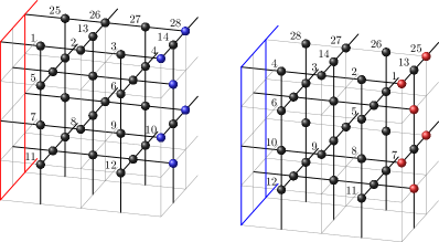
We can generalize the conditions for optimizing the 3D cluster state construction procedure using emitters, which does not allow for interruption. Firstly, considering the fact that two emitters should interact to entangle the qubits in two different subgraphs, we need an even number of emitters; if not, an incrementation of one index for the subgraph has to be interrupted. Secondly, must be an integer to ensure that the number of qubits in different slabs is the same. In Section IV, we simulated all the 3D cluster state construction procedure satisfying these two conditions.
IV Fault-tolerant error correction using multiple emitters
IV.1 Threshold
In this Section, we study the thresholds for Protocols M1 and M2. Note that the main difference between these protocols and the single-emitter protocols [Section II] is the presence of CZ gate between the ancilla qubits. We will employ the standard depolarizing noise model for this gate as well [Eq. (9)].
Physically, the entangling gate used between the emitters may use a physical mechanism different from the one used for the gate between the emitter and the photon. For instance, the gate between the emitters may be based on an exchange interaction Loss and DiVincenzo (1998) whereas the the gate between the emitter and the photon involves an optical interaction that exploits quantum dot’s ability to emit and absorb single photon Volz et al. (2014); Sipahigil et al. (2016); Goban et al. (2014); Tiecke et al. (2014); Reiserer et al. (2014). Therefore, it is reasonable to study an anisotropic error model that treats the entangling gate between the emitters differently from the rest. For this reason, we tune the ratio between the two sources of error. More precisely, we denote the noise strength of the gate between the emitters as and the noise strength of the rest as [Eq. (9)]. We studied the threshold under different ratios of .
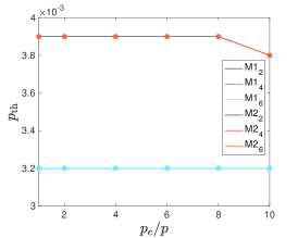
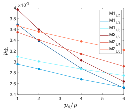
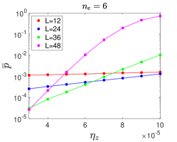
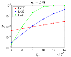
Here are the details of our numerical study. We chose a range of values of for different number of emitters, using Protocol M1 and M2. Each data point is averaged over samples. The thresholds were obtained by fitting the data to the ansatz in Eq. (10). The results are shown in Figure 8. The top figure shows the threshold when the number of emitters is a constant independent of the code distance. The bottom figure shows the threshold when the number of emitters scales linearly with the code distance.
The most striking conclusion from Figure 8 is that the threshold value barely changes even if the the ratio approaches , provided that is a constant independent of the code distance [Figure 8, top]. This suggests that our scheme can tolerate a significantly higher error rate for the entangling gate between the emitters compared to the other sources of error. Our result is consistent with a recent study which also demonstrated a high tolerance against an error at the interface in a modular approach to fault-tolerantly correcting errors using the surface code Ramette et al. (2023). While the underlying error model is not identical, the analytical arguments in Ref. Ramette et al. (2023) can explain our observation qualitatively.
When the number of emitters scales linearly with the code distance, we do observe a decrease in threshold as increases. Nonetheless, the order of magnitude of the threshold remains the same.
IV.2 Delay line error
We now include the effect of the delay line errors. The error model associated with this error is identical to the one used in Section II.3.2. For the CZ gate between the ancilla qubits, we assume the error rate is equal to the error rate of the other circuit-level noises, i.e., .
As we discussed already in Section II, in the presence of a delay line error, there is no threshold. A more relevant question was how one can optimally choose the length of the delay line, given the error rate per unit length , and what the corresponding optimal logical rate is.
Here, we aim to understand the same question but instead focusing on how to obtain the logical error rate in terms of and . There are two regimes of interest, depending on whether the number of emitters is small or large, compared to .
For a fixed , the strength of the delay line error on each qubit scales linearly with . Therefore, in order to ensure that the amount of accumulated error is smaller than the threshold (which is necessary for error suppression), the maximum length one can have is . Recalling that the logical error rate decays exponentially with , we expect the optimal logical error rate to be
| (17) |
where and are positive constants. On the other hand, we can also consider the case in which scales linearly with , i.e., for some integer . In this case, the maximum length one can have is . Then the optimal logical error rate would be
| (18) |
| () | () | () | |
|---|---|---|---|
| () | () | () | |
|---|---|---|---|
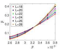
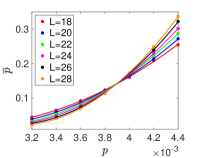
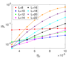
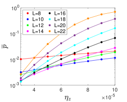
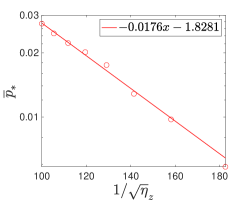
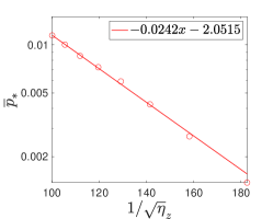
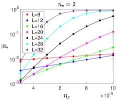
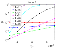
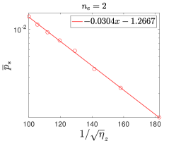
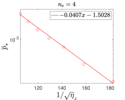
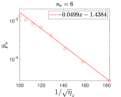
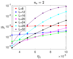
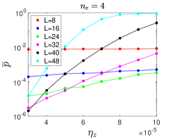
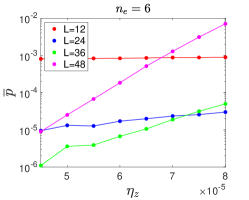
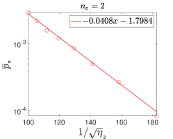
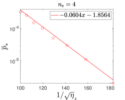
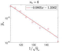
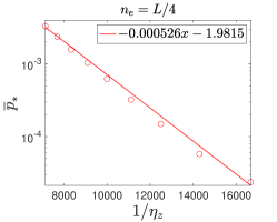
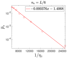
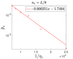
Now we discuss the results of our simulations. We will primarily focus on the effect of dephasing error, and only briefly mention about the loss error simulation at the very end of this Section. We first comment on the case of [Eq. (17)]. We considered using , and samples per data point, using the circuit-level depolarizing noise of . (Larger number of required larger sample size because the logical error rates obtained is lower.) All these data points were well-described by the values of and for M1 and and for M2, respectively; see Figure 9 and 10.333More precisely, for M1, we obtained for , respectively. For M2, we obtained for , respectively. We remark that the values of and for algorithms M1 and M2 are similar to those in S1 and S2, respectively (corresponding to the case). Therefore, we can conclude that the ansatz in Eq. (17) adequately describes the scaling behavior of the logical error rate. Using this equation, we listed the requisite dephasing error rates to achieve targeted logical error rates of are summarized in Table 2 (top), (bottom).
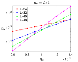
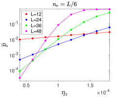
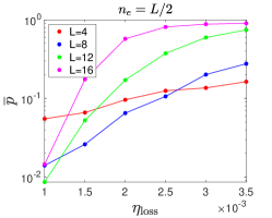
For the case of , we chose and employed Protocol M1 [Figure 11].444While we carried out the same simulation for Protocol M2 as well, even with samples we could not determine the minimum logical error rate . In particular, we could not obtain the constants in Eq. (18). Nonetheless, we found the break-even point with to be greater than . Examining the plots presented in Figure 11 (bottom), we observe a linear relationship between and for . The values of and obtained were and for all the cases.555More precisely, we obtained for . The requisite dephasing error rates to achieve targeted logical error rates of are summarized in Table 3.
We remark that for , the result of our simulation was inconsistent with Eq. (18); see Figure 12 (left). More precisely, we obtained , which is different from the other values of (which were ). We believe this discrepancy is coming from the fact that there are no qubits lying in the interior of the slab for (unlike ).
| () | () | () | |
|---|---|---|---|
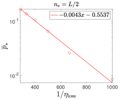
Lastly, let us briefly mention the result of our loss error simulation. To that end, we considered the phenomenological noise model in Eq. (12), employing the decoding algorithm in Ref. Barrett and Stace (2010); see Figure 12 (right). Each data point is obtained from samples. The only result we present here are the case of , which yields the lowest possible logical error rate out of all possible choice of we discuss; see Section IV.3.

IV.3 Comparison: single- vs. multi-emitter
In this Section, we discuss what kind of improvements the multi-emitter protocol [Section III] provides over the single-emitter protocol [Section II]. Recall that the optimal logical error rate improves as increases [Section IV.2]. Since the largest possible value of is , we focus on comparing this case to the single-emitter protocol.
| dephasing error() | loss error() | |
|---|---|---|
In Table 4, we listed the dephasing and loss error rates needed to achieve the target logical error rates of . Comparing these results to the simulation results for the single-emitter protocol [Table 1 (top)], we observe an approximately a ten-fold improvement (for the dephasing error) and a five-fold improvement (for the loss error) for achieving the break-even point (defined as ). Even greater improvements are achieved for lower target logical error rates.
V Discussion
In this paper, we propose protocols for constructing a cluster state using a linear array of emitters. Our key observation is that the the protocol in Ref. Wan et al. (2021) can be generalized to a protocol involving multiple emitters with a simple modification: an intermittent application of CZ gates between pairs of emitters.
Such a modification reduces the amount of time each photon travels in the delay line, thereby improving the logical error rate overall. Although having a larger number of emitters may be more challenging than having only a single emitter, there are several reasons to prefer the multi-emitter protocol over the single-emitter protocol. The primary reason is the improved logical error rate. If one compares the delay line error rate needed to achieve the same logical error rate, the multi-emitter protocol [Table 4] outperforms the single-emitter protocol [Table 1] by a factor of at least , depending on the error model and the target logical error rate. Second, our protocol enjoys a high tolerance against two-qubit gates applied between the emitters. The thresholds for such gates were shown to be at least ten-fold larger than the threshold for the other gates [Figure 8]. Lastly, the number of emitters is a tunable parameter in our scheme, and even a modest improvement in the number of emitters immediately yield improvements in the logical error rate [Section III.2].
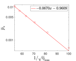
An interesting question is whether an error suppression can be demonstrated using our scheme in a realistic experiment. More specifically, we would define error suppression as an outcome in which the logical error rate after the error correction is lower than the physical error rate. Setting the physical error rate of , assuming the dominant source of error in the delay line is loss, we would obtain the break-even point () of . This is lower than what the state-of-the-art delay line can achieve, e.g., Tamura et al. (2018). Therefore, our scheme, in the form presented in this paper, will not be able to achieve error suppression, even if we assume we used the state-of-the-art delay lines.
However, we think there are a few simple modifications in the protocol that can make the break-even point (for the delay line error) higher. Most importantly, we think simply changing our boundary condition to the open boundary condition will improve the result substantially. To see why, let us remark that our setup differs from that of Ref. Wan et al. (2021); the latter used an open boundary condition whereas we used a periodic boundary condition. The details about the loss error model is also different. While we obtained a similar threshold in spite of these differences, their sub-threshold behaviors are more markedly different; we found the loss error rates needed in our protocol to achieve specific target logical error rates were lower than that of Ref. Wan et al. (2021) by a factor of .
What would happen if we change the boundary condition to the open boundary condition? We conjecture that the scaling form of the optimal logical error rate [Eq. (17) and (18)] would be still valid even under such a condition, though with different constants. Let us briefly justify it. First, we remark that we are assuming that the circuit-level noise remains at , which is below the threshold (in the absence of other error sources). The additional error comes from the qubit loss, which is proportional to for every qubit, for both error models. While the details about this loss error model is different, this difference only causes a few additional gates for each data qubit. More precisely, in Ref. Wan et al. (2021), the loss can occur during the construction of the cluster state whereas in our case the loss occurs at the very end of the protocol. When qubit loss occurs during the construction of the cluster state, all subsequent operations acting on the lost data qubit become identity operators Wan et al. (2021). Therefore, in the entire procedure of gate operations, the loss error model where qubit loss occurs at the very end of the protocol requires only a few additional gate operations compared to the model where qubit loss occurs during the construction of the cluster state. While these are clearly different error models, they can be both described by some local error model. As such, we do not expect the logical error rate scaling form to be different.
The constants in Eq. (17) can be inferred from the Ref. Wan et al. (2021). The scaling relation in Ref. Wan et al. (2021) would correspond to the case in Eq. (17), yielding and . Then, even with the use of two emitters (), the requisite loss error rate to reach the break-even point becomes , which is strictly larger than the reported error rate of Tamura et al. (2018). Therefore, provided that our assumption on the error scaling is correct, we are led to the conclusion that error suppression can be demonstrated with just two emitters and four delay lines. This is more demanding than what was originally envisioned in Ref. Wan et al. (2021), but only barely.
Of course, the picture we described so far is too simplistic. For one thing, there can be an additional insertion error occurring as the photon moves in and out of the delay line. Moreover, there are other schemes, such as the one using concatenation, which were shown to improve the noise tolerance Li et al. (2023). In order to more accurately assess the experimental prospect of our multi-emitter protocol, it is important to accurately model these sources of error and employ the error correction schemes that are adept at correcting such errors.
Acknowledgements.
We thank Hassan Shapourian and Alireza Shabani for useful discussions and Yun-Tak Oh for helping with simulations. J. K. was supported by the education and training program of the Quantum Information Research Support Center, funded through the National research foundation of Korea (NRF) by the Ministry of science and ICT (MSIT) of the Korean government(No.2021M3H3A103657313). J.H.H. was supported by the National Research Foundation of Korea (NRF) grant funded by the Korea government (MSIT) (No. 2023R1A2C1002644). I. K. was supported by the Cisco Research Gift Program.References
- Gottesman (1998a) D. Gottesman, Phys. Rev. A 57, 127 (1998a), URL https://link.aps.org/doi/10.1103/PhysRevA.57.127.
- Gottesman (1998b) D. Gottesman (1998b), URL https://arxiv.org/abs/quant-ph/9807006.
- Gottesman (2009) D. Gottesman, An introduction to quantum error correction and fault-tolerant quantum computation (2009), URL https://arxiv.org/abs/0904.2557.
- Kitaev (2003) A. Kitaev, Annals of Physics 303, 2 (2003), ISSN 0003-4916, URL https://www.sciencedirect.com/science/article/pii/S0003491602000180.
- Aharonov and Ben-Or (2008) D. Aharonov and M. Ben-Or, SIAM Journal on Computing 38, 1207 (2008), eprint https://doi.org/10.1137/S0097539799359385, URL https://doi.org/10.1137/S0097539799359385.
- Knill et al. (1998) E. Knill, R. Laflamme, and W. H. Zurek, Science 279, 342 (1998), eprint https://www.science.org/doi/pdf/10.1126/science.279.5349.342, URL https://www.science.org/doi/abs/10.1126/science.279.5349.342.
- Barends et al. (2014) R. Barends, J. Kelly, A. Megrant, A. Veitia, D. Sank, E. Jeffrey, T. C. White, J. Mutus, A. G. Fowler, B. Campbell, et al., Nature 508, 500 (2014), ISSN 1476-4687, URL https://doi.org/10.1038/nature13171.
- Arute et al. (2019) F. Arute, K. Arya, R. Babbush, D. Bacon, J. C. Bardin, R. Barends, R. Biswas, S. Boixo, F. G. S. L. Brandao, D. A. Buell, et al., Nature 574, 505 (2019), ISSN 1476-4687, URL https://doi.org/10.1038/s41586-019-1666-5.
- Harty et al. (2014) T. P. Harty, D. T. C. Allcock, C. J. Ballance, L. Guidoni, H. A. Janacek, N. M. Linke, D. N. Stacey, and D. M. Lucas, Phys. Rev. Lett. 113, 220501 (2014), URL https://link.aps.org/doi/10.1103/PhysRevLett.113.220501.
- Ballance et al. (2016) C. J. Ballance, T. P. Harty, N. M. Linke, M. A. Sepiol, and D. M. Lucas, Phys. Rev. Lett. 117, 060504 (2016), URL https://link.aps.org/doi/10.1103/PhysRevLett.117.060504.
- Monroe and Kim (2013) C. Monroe and J. Kim, Science 339, 1164 (2013), eprint https://www.science.org/doi/pdf/10.1126/science.1231298, URL https://www.science.org/doi/abs/10.1126/science.1231298.
- Madsen et al. (2022) L. S. Madsen, F. Laudenbach, M. F. Askarani, F. Rortais, T. Vincent, J. F. F. Bulmer, F. M. Miatto, L. Neuhaus, L. G. Helt, M. J. Collins, et al., Nature 606, 75 (2022), ISSN 1476-4687, URL https://doi.org/10.1038/s41586-022-04725-x.
- Levine et al. (2019) H. Levine, A. Keesling, G. Semeghini, A. Omran, T. T. Wang, S. Ebadi, H. Bernien, M. Greiner, V. Vuletić, H. Pichler, et al., Phys. Rev. Lett. 123, 170503 (2019), URL https://link.aps.org/doi/10.1103/PhysRevLett.123.170503.
- Norcia et al. (2018) M. A. Norcia, A. W. Young, and A. M. Kaufman, Phys. Rev. X 8, 041054 (2018), URL https://link.aps.org/doi/10.1103/PhysRevX.8.041054.
- Saskin et al. (2019) S. Saskin, J. T. Wilson, B. Grinkemeyer, and J. D. Thompson, Phys. Rev. Lett. 122, 143002 (2019), URL https://link.aps.org/doi/10.1103/PhysRevLett.122.143002.
- Covey et al. (2019) J. P. Covey, I. S. Madjarov, A. Cooper, and M. Endres, Phys. Rev. Lett. 122, 173201 (2019), URL https://link.aps.org/doi/10.1103/PhysRevLett.122.173201.
- Fowler et al. (2012) A. G. Fowler, M. Mariantoni, J. M. Martinis, and A. N. Cleland, Phys. Rev. A 86, 032324 (2012), URL https://link.aps.org/doi/10.1103/PhysRevA.86.032324.
- Tremblay et al. (2022) M. A. Tremblay, N. Delfosse, and M. E. Beverland, Phys. Rev. Lett. 129, 050504 (2022), URL https://link.aps.org/doi/10.1103/PhysRevLett.129.050504.
- Delfosse et al. (2021) N. Delfosse, M. E. Beverland, and M. A. Tremblay, Bounds on stabilizer measurement circuits and obstructions to local implementations of quantum ldpc codes (2021), eprint 2109.14599.
- Strikis and Berent (2023) A. Strikis and L. Berent, PRX Quantum 4 (2023), ISSN 2691-3399, URL http://dx.doi.org/10.1103/PRXQuantum.4.020321.
- Xu et al. (2023) Q. Xu, J. P. B. Ataides, C. A. Pattison, N. Raveendran, D. Bluvstein, J. Wurtz, B. Vasic, M. D. Lukin, L. Jiang, and H. Zhou, Constant-overhead fault-tolerant quantum computation with reconfigurable atom arrays (2023), eprint 2308.08648.
- Acharya et al. (2022) R. Acharya, I. Aleiner, R. Allen, T. Andersen, M. Ansmann, F. Arute, K. Arya, A. Asfaw, J. Atalaya, R. Babbush, et al., Nature (2022), URL https://dx.doi.org/10.1038/s41586-022-05434-1.
- Ryan-Anderson et al. (2021) C. Ryan-Anderson, J. Bohnet, K. Lee, D. Gresh, A. Hankin, J. Gaebler, D. Francois, A. Chernoguzov, D. Lucchetti, N. C. Brown, et al., Physical Review X (2021), URL https://dx.doi.org/10.1103/physrevx.11.041058.
- Ryan-Anderson et al. (2022) C. Ryan-Anderson, N. C. Brown, M. S. Allman, B. Arkin, G. Asa-Attuah, C. Baldwin, J. Berg, J. Bohnet, S. Braxton, N. Burdick, et al., arXiv (2022), URL https://arxiv.org/abs/2208.01863.
- Bluvstein et al. (2023) D. Bluvstein, S. Evered, A. A. Geim, S. H. Li, H. Zhou, T. Manovitz, S. Ebadi, M. Cain, M. Kalinowski, D. Hangleiter, et al., Nature (2023), URL https://dx.doi.org/10.1038/s41586-023-06927-3.
- Reiher et al. (2016) M. Reiher, N. Wiebe, K. Svore, D. Wecker, and M. Troyer, Proceedings of the National Academy of Sciences (2016), URL https://dx.doi.org/10.1073/pnas.1619152114.
- Lee et al. (2020) J. Lee, D. Berry, C. Gidney, W. Huggins, J. McClean, N. Wiebe, and R. Babbush, PRX Quantum (2020), URL https://dx.doi.org/10.1103/PRXQuantum.2.030305.
- von Burg et al. (2020) V. von Burg, G. Low, T. Häner, D. S. Steiger, M. Reiher, M. Roetteler, and M. Troyer, Physical Review Research (2020), URL https://dx.doi.org/10.1103/PhysRevResearch.3.033055.
- Raussendorf and Briegel (2001) R. Raussendorf and H. J. Briegel, Phys. Rev. Lett. 86, 5188 (2001), URL https://link.aps.org/doi/10.1103/PhysRevLett.86.5188.
- Raussendorf et al. (2003) R. Raussendorf, D. E. Browne, and H. J. Briegel, Phys. Rev. A 68, 022312 (2003), URL https://link.aps.org/doi/10.1103/PhysRevA.68.022312.
- Nielsen (2004) M. A. Nielsen, Phys. Rev. Lett. 93, 040503 (2004), URL https://link.aps.org/doi/10.1103/PhysRevLett.93.040503.
- Walther et al. (2005) P. Walther, K. J. Resch, T. Rudolph, E. Schenck, H. Weinfurter, V. Vedral, M. Aspelmeyer, and A. Zeilinger, Nature 434, 169 (2005), ISSN 1476-4687, URL https://doi.org/10.1038/nature03347.
- Lindner and Rudolph (2009) N. H. Lindner and T. Rudolph, Phys. Rev. Lett. 103, 113602 (2009), URL https://link.aps.org/doi/10.1103/PhysRevLett.103.113602.
- Economou et al. (2010) S. E. Economou, N. Lindner, and T. Rudolph, Phys. Rev. Lett. 105, 093601 (2010), URL https://link.aps.org/doi/10.1103/PhysRevLett.105.093601.
- Yokoyama et al. (2013) S. Yokoyama, R. Ukai, S. C. Armstrong, C. Sornphiphatphong, T. Kaji, S. Suzuki, J.-i. Yoshikawa, H. Yonezawa, N. C. Menicucci, and A. Furusawa, Nature Photonics 7, 982 (2013), ISSN 1749-4893, URL https://doi.org/10.1038/nphoton.2013.287.
- Yoshikawa et al. (2016) J.-i. Yoshikawa, S. Yokoyama, T. Kaji, C. Sornphiphatphong, Y. Shiozawa, K. Makino, and A. Furusawa, APL Photonics 1, 060801 (2016), eprint https://doi.org/10.1063/1.4962732, URL https://doi.org/10.1063/1.4962732.
- Schwartz et al. (2016) I. Schwartz, D. Cogan, E. R. Schmidgall, Y. Don, L. Gantz, O. Kenneth, N. H. Lindner, and D. Gershoni, Science 354, 434 (2016), eprint https://www.science.org/doi/pdf/10.1126/science.aah4758, URL https://www.science.org/doi/abs/10.1126/science.aah4758.
- Pichler et al. (2017) H. Pichler, S. Choi, P. Zoller, and M. D. Lukin, Proceedings of the National Academy of Sciences 114, 11362 (2017), eprint https://www.pnas.org/doi/pdf/10.1073/pnas.1711003114, URL https://www.pnas.org/doi/abs/10.1073/pnas.1711003114.
- Larsen et al. (2019) M. V. Larsen, X. Guo, C. R. Breum, J. S. Neergaard-Nielsen, and U. L. Andersen, Science 366, 369 (2019), eprint https://www.science.org/doi/pdf/10.1126/science.aay4354, URL https://www.science.org/doi/abs/10.1126/science.aay4354.
- Asavanant et al. (2019) W. Asavanant, Y. Shiozawa, S. Yokoyama, B. Charoensombutamon, H. Emura, R. N. Alexander, S. Takeda, J. ichi Yoshikawa, N. C. Menicucci, H. Yonezawa, et al., Science 366, 373 (2019), eprint https://www.science.org/doi/pdf/10.1126/science.aay2645, URL https://www.science.org/doi/abs/10.1126/science.aay2645.
- Wan et al. (2021) K. Wan, S. Choi, I. H. Kim, N. Shutty, and P. Hayden, PRX Quantum 2, 040345 (2021), URL https://link.aps.org/doi/10.1103/PRXQuantum.2.040345.
- Shi and Waks (2021) Y. Shi and E. Waks, Phys. Rev. A 104, 013703 (2021), URL https://link.aps.org/doi/10.1103/PhysRevA.104.013703.
- Ferreira et al. (2022) V. S. Ferreira, G. Kim, A. Butler, H. Pichler, and O. Painter, Deterministic generation of multidimensional photonic cluster states with a single quantum emitter (2022), eprint 2206.10076.
- Roh et al. (2023) C. Roh, G. Gwak, Y.-D. Yoon, and Y.-S. Ra, Generation of three-dimensional cluster entangled state (2023), eprint 2309.05437.
- Bartolucci et al. (2021) S. Bartolucci, P. Birchall, H. Bombin, H. Cable, C. Dawson, M. Gimeno-Segovia, E. R. Johnston, K. Kieling, N. H. Nickerson, M. Pant, et al., Nature Communications 12 (2021), URL https://dx.doi.org/10.1038/s41467-023-36493-1.
- Bombin et al. (2021) H. Bombin, I. H. Kim, D. Litinski, N. H. Nickerson, M. Pant, F. Pastawski, S. Roberts, and T. Rudolph, Interleaving: Modular architectures for fault-tolerant photonic quantum computing (2021), accessed: 2023-12-24, eprint 2103.08612, URL https://arxiv.org/abs/2103.08612.
- Bourassa et al. (2021) J. Bourassa, R. N. Alexander, M. Vasmer, A. Patil, I. Tzitrin, T. Matsuura, D. Su, B. Baragiola, S. Guha, G. Dauphinais, et al., Quantum 5, 392 (2021), URL https://dx.doi.org/10.22331/Q-2021-02-04-392.
- Tzitrin et al. (2021) I. Tzitrin, T. Matsuura, R. N. Alexander, G. Dauphinais, J. Bourassa, K. K. Sabapathy, N. Menicucci, and I. Dhand, PRX Quantum 2, 040353 (2021), URL https://dx.doi.org/10.1103/PRXQuantum.2.040353.
- Raussendorf et al. (2005) R. Raussendorf, S. Bravyi, and J. Harrington, Phys. Rev. A 71, 062313 (2005), URL https://link.aps.org/doi/10.1103/PhysRevA.71.062313.
- Raussendorf et al. (2006) R. Raussendorf, J. Harrington, and K. Goyal, Annals of Physics 321, 2242 (2006), ISSN 0003-4916, URL https://www.sciencedirect.com/science/article/pii/S0003491606000236.
- Raussendorf et al. (2007) R. Raussendorf, J. Harrington, and K. Goyal, New Journal of Physics 9, 199 (2007), URL https://doi.org/10.1088/1367-2630/9/6/199.
- Tamura et al. (2018) Y. Tamura, H. Sakuma, K. Morita, M. Suzuki, Y. Yamamoto, K. Shimada, Y. Honma, K. Sohma, T. Fujii, and T. Hasegawa, Journal of Lightwave Technology 36, 44 (2018), URL https://opg.optica.org/jlt/abstract.cfm?uri=jlt-36-1-44.
- Xue et al. (2021) X. Xue, M. Russ, N. Samkharadze, B. Undseth, A. Sammak, G. Scappucci, and L. Vandersypen, Nature (2021), URL https://dx.doi.org/10.1038/s41586-021-04273-w.
- Noiri et al. (2022) A. Noiri, J. Yoneda, T. Nakajima, K. Takeda, T. Kodera, T. Otsuka, R. Li, S. D. Bartlett, A. Ludwig, A. D. Wieck, et al., Nature (2022), URL https://dx.doi.org/10.1038/s41586-021-04276-7.
- Mills et al. (2022) A. R. Mills, C. Guinn, M. Gullans, A. Sigillito, M. Feldman, E. Nielsen, and J. Petta, Science Advances (2022), URL https://dx.doi.org/10.1126/sciadv.abn5130.
- Madzik et al. (2022) M. T. Madzik, S. G. J. Philips, S. V. Amitonov, M. Russ, N. Kalhor, W. I. L. Lawrie, D. Brousse, A. Sammak, M. Veldhorst, G. Scappucci, et al., Nature (2022), URL https://dx.doi.org/10.1038/s41586-021-04275-8.
- Philips et al. (2022) S. Philips, M. Madzik, S. Amitonov, S. L. de Snoo, M. Russ, N. Kalhor, C. Volk, W. Lawrie, D. Brousse, L. Tryputen, et al., Nature (2022), URL https://dx.doi.org/10.1038/s41586-022-05117-x.
- Dennis et al. (2002) E. Dennis, A. Kitaev, A. Landahl, and J. Preskill, Journal of Mathematical Physics 43, 4452 (2002), eprint https://doi.org/10.1063/1.1499754, URL https://doi.org/10.1063/1.1499754.
- Higgott and Gidney (2022) O. Higgott and C. Gidney, Pymatching v2, https://github.com/oscarhiggott/PyMatching (2022).
- Gidney (2021) C. Gidney, Quantum 5, 497 (2021), ISSN 2521-327X, URL https://doi.org/10.22331/q-2021-07-06-497.
- Shapourian and Shabani (2022) H. Shapourian and A. Shabani, Quantum (2022), URL https://dx.doi.org/10.22331/q-2023-03-02-935.
- Barrett and Stace (2010) S. D. Barrett and T. M. Stace, Phys. Rev. Lett. 105, 200502 (2010), URL https://link.aps.org/doi/10.1103/PhysRevLett.105.200502.
- Loss and DiVincenzo (1998) D. Loss and D. P. DiVincenzo, Physical Review A 57, 120 (1998), URL https://link.aps.org/doi/10.1103/PhysRevA.57.120.
- Volz et al. (2014) J. Volz, M. Scheucher, C. Junge, and A. Rauschenbeutel, Nature Photonics 8, 965 (2014), URL https://www.nature.com/articles/nphoton.2014.253.
- Sipahigil et al. (2016) A. Sipahigil, R. E. Evans, D. D. Sukachev, M. J. Burek, J. Borregaard, M. K. Bhaskar, C. T. Nguyen, J. L. Pacheco, H. A. Atikian, C. Meuwly, et al., Science 354, 847 (2016), URL https://science.sciencemag.org/content/354/6314/847.
- Goban et al. (2014) A. Goban, C.-L. Hung, S.-P. Yu, J. Hood, J. Muniz, J. Lee, M. Martin, A. McClung, K. Choi, D. Chang, et al., Nature Communications 5 (2014), URL https://www.nature.com/articles/ncomms4808.
- Tiecke et al. (2014) T. G. Tiecke, J. D. Thompson, N. P. de Leon, L. R. Liu, V. Vuletić, and M. D. Lukin, Nature 508, 241 (2014), URL https://www.nature.com/articles/nature13188.
- Reiserer et al. (2014) A. Reiserer, N. Kalb, G. Rempe, and S. Ritter, Nature 508, 237 (2014), URL https://www.nature.com/articles/nature13177.
- Ramette et al. (2023) J. Ramette, J. Sinclair, N. P. Breuckmann, and V. Vuletić, Fault-tolerant connection of error-corrected qubits with noisy links (2023), eprint 2302.01296.
- Li et al. (2023) Z. Li, I. Kim, and P. Hayden, Quantum 7, 1089 (2023), ISSN 2521-327X, URL https://doi.org/10.22331/q-2023-08-22-1089.