All-Pass Readout for Robust and Scalable Quantum Measurement
Abstract
Robust and scalable multiplexed qubit readout will be essential to the realization of a fault-tolerant quantum computer. To this end, we propose and demonstrate transmission-based dispersive readout of a superconducting qubit using an all-pass resonator that preferentially emits readout photons in one direction. This is in contrast to typical readout schemes, which intentionally mismatch the feedline at one end so that the readout signal preferentially decays toward the output. We show that this intentional mismatch creates scaling challenges, including larger spread of effective resonator linewidths due to non-ideal impedance environments and added infrastructure for impedance matching. Our proposed “all-pass readout” architecture avoids the need for intentional mismatch and aims to enable reliable, modular design of multiplexed qubit readout, thus improving the scaling prospects of quantum computers. We design and fabricate an all-pass readout resonator that demonstrates insertion loss below at the readout frequency and a maximum insertion loss of across its full bandwidth for the lowest three states of a transmon qubit. We demonstrate qubit readout with an average single-shot fidelity of 98.1% in ; to assess the effect of larger dispersive shift, we implement a shelving protocol and achieve a fidelity of 99.0% in .
I Introduction
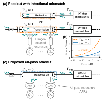
Dispersive readout [1, 2, 3], broadband parametric amplifiers [4, 5], and Purcell filtering [6, 7, 8] have made it possible to perform multiplexed single-shot readout of superconducting qubit systems with high fidelity [9, 10]. Such capabilities will be critical for any application requiring real-time feedback, such as quantum error correction (QEC) [11, 12, 10]. In multiplexed readout, maximizing the collection of photons encoded with qubit information is critical to improving the signal-to-noise ratio (SNR). As a result, the feedline is often intentionally interrupted at one end (the “input”) with a wideband mismatch with near-total reflection so that the readout signal preferentially decays from the resonators toward the detection apparatus (the “output”) [8, 9, 10, 13]. In a transmission-based readout configuration, this intentional mismatch takes the form of an input capacitance [9, 10, 8]; in a reflection-based readout configuration, one end of the feedline is terminated in an open [13]. However, we show that intentional mismatch creates standing waves that both significantly worsen the spread of resonator linewidths and require added infrastructure for impedance matching. We detail these challenges in Sec. II; a summary is shown in Table 1. Despite its disadvantages, the intentional use of mismatch in the feedline has thus far been ubiquitous and essential to enable directional decay of the readout signal and maximize SNR [9, 10, 13, 8]. Thus, an attractive yet unexplored research direction would investigate readout schemes that avoid intentional mismatch while preserving the directional decay of the readout signal.
Here, we propose and demonstrate “all-pass readout,” a transmission-based scheme in which the readout resonator demonstrates preferential directional emission of photons encoded with qubit information, thus avoiding the need for intentional mismatch. In Sec. III, we present a model for an all-pass resonator coupled to a transmon qubit. We experimentally demonstrate all-pass performance with the fabricated device detailed in Sec. IV and demonstrate high-fidelity single-shot readout in Sec. V.
II Limitations of Standing Waves in Readout
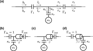
Cyclic protocols for quantum error correction, such as the surface code, require reliable measurement of all data and syndrome qubits within a given cycle [14]. As a result, robust control of the resonator linewidth is of critical importance. If is too large, the qubit lifetime can be shortened due to the Purcell effect [6, 8, 7]. Too small of is also problematic since the repetition rate of cyclic protocols is limited by the qubit with the slowest readout [14]. In practice, it is common to see significant variation in the resonator linewidth; this has previously been attributed to off-chip impedance mismatches [13, 15, 16]. A multiplexed readout scheme with intentional mismatch is depicted in Fig. 1a, where hanger-coupled resonators are coupled to a feedline, and the intentional mismatch is represented by an input capacitance (in transmission [9, 10, 8]) or as an open (in reflection [13].) In Fig. 1a, we depict resonators directly coupled to the feedline, but note that the variation of effective linewidth extends to designs with bandpass Purcell filters. In the following analysis, we show that intentional mismatch worsens variation by increasing the sensitivity of the resonator linewidth to non-ideal impedance environments, such as off-chip mismatches and on-chip non-uniformities.
First, we show how intentional mismatch worsens the variation in resonator linewidth as a result of off-chip mismatch, where the spread is related to the voltage standing wave ratio, given by . The output-side reflection coefficient depends on the matching performance of off-chip components, such as the sample package, isolators, and filters. For a system with intentional mismatch (), the ratio of the largest to smallest possible linewidths is given by the square of VSWR (see Appendix B.1)
| (1) |
This was confirmed experimentally in [13], where a spread in of was measured for . From (1), a clear way to mitigate spread in is to improve matching performance at the output. As a complementary approach, we could also improve matching at the input by removing the intentional mismatch. If , the scaling of is now given by (see Appendix B.2)
| (2) |
As shown in Fig. 1b, this is a square-root reduction in compared to (1). The key advantage to this approach is that attenuators can be used for matching on the input side to minimize (see Fig. 1c). In contrast, attenuators cannot typically be used on the output side, since minimization of pre-amplification losses is critical for maximizing measurement efficiency [17].
| No Intentional Mismatch | Intentional Mismatch | All-Pass Readout | |
|---|---|---|---|
| Input-side reflection | |||
| Directional decay of readout signal? | No | Yes | Yes |
| Spread in due to off-chip mismatches | |||
| Sensitivity of to chip non-uniformities | Low | High | Low |
| Need for amplifier impedance matching | Low | High | Low |
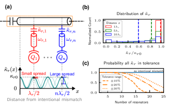
Next, we show that intentional mismatch also makes the resonator linewidth highly sensitive to non-uniformities in the effective permittivity as seen by a coplanar waveguide across a chip. Non-uniformities are especially prevalent in flip-chip processors, where inter-chip spacing variation and nonlinear chip deformations on the order of can cause resonator frequencies to vary by a few percent across a chip [15, 18]. We consider the circuit in Fig. 2a, where multiplexed resonators are positioned along a feedline interrupted by intentional mismatch (e.g., an input capacitance). For a resonator at a distance from the intentional mismatch, the fabricated linewidth is approximated by (see Appendix B.3)
| (3) |
where is the largest possible linewidth, is the resonator wavelength, is the effective permittivity of the feedline between the input capacitance and the resonator, and is the effective permittivity of the resonator. To maximize coupling to the waveguide, we position resonators at multiples of half-wavelength, similar to [9]. As visualized in Fig. 2a, due to the standing wave formed by the intentional mismatch, becomes more sensitive to non-uniformities in permittivity () at farther distances . To quantify this effect, we assume that the error for each resonator obeys a normal distribution with a mean of 1 (no error) and a relative standard deviation of 1.5% (e.g., a shift of for a resonator). In Fig. 2b, we plot histograms of for increasing distances . In Fig. 2c, we plot the probability that all fabricated are within a given tolerance as a function of the number of resonators, assuming that two resonators are coupled at each half-wavelength , similar to [9]. Even assuming a generous tolerance range of for , reliable fabrication of more than 15 multiplexed resonators becomes impractical. In reality, the situation is even worse due to added variation from off-chip mismatches. Because flip-chip processors are an attractive platform for the further scaling of quantum computers, it will be critical to make the resonator linewidth insensitive to on-chip non-uniformities moving forward. Removing the intentional mismatch would achieve this goal (see Fig. 2c). Moreover, this would make quantum processor design far more modular, as flexible placement of resonator-qubit blocks is possible.
As a final comment, we note that intentional mismatch also impedes the scaling of quantum computers by requiring the addition of nonreciprocal components to impedance match to downstream amplifiers [19, 20, 9, 21]. We refer the reader to Appendix C for further details.
III Model of All-Pass Readout
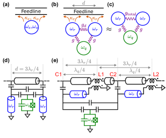
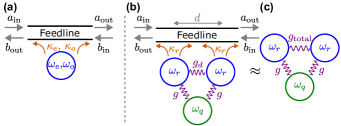
In sharp contrast to an overcoupled hanger-coupled readout resonator, which exhibits total reflection on resonance, an all-pass readout resonator instead approaches total transmission on resonance (). We can understand how all-pass behavior arises by considering a resonator with both an even and an odd mode coupled to a waveguide (Fig. 3a). The transmission is given by (see Appendix D)
| (4) |
where () is the even (odd) mode frequency and () is the even (odd) mode linewidth. The two modes will be degenerate if they have equal frequencies and equal linewidths, i.e., and . In this special case, (4) becomes
| (5) |
which achieves the desired all-pass behavior [23]. This can be understood by noting that at , we have .
With these conditions for all-pass behavior in mind, we design a resonator with even and odd modes to perform readout of a qubit (see Fig. 3b). A transmon qubit mode with frequency and charging energy is coupled symmetrically to two identical resonator modes and with frequency . The resonators are coupled to a waveguide with linewidth and separated by distance . The qubit-resonator coupling rates have magnitude , and the direct resonator-resonator coupling rate has magnitude . We can sum the direct and waveguide-mediated coupling rates and simplify Fig. 3b as Fig. 3c, where (see Appendix D). The Hamiltonian of Fig. 3c is approximately represented in the Fock basis by
| (6) | ||||
After a transformation of basis and truncation of the transmon to the first two energy levels (see Appendix E), we can derive the dispersive Hamiltonian
| (7) |
where the dressed qubit frequency , even mode frequency , odd mode frequency , and effective dispersive shift are approximated by
| (8) |
| (9) |
| (10) |
and
| (11) |
where we define the qubit-resonator detuning as . Note that the even mode experiences a dispersive shift of , whereas the odd mode does not. This is because the qubit is positioned at the node of the odd mode of this system. Thus, the effective frequency shift is .
Recall that all-pass behavior is obtained when the even and odd modes are degenerate. Neglecting the dispersive shift for the moment, we see that when . Intuitively, all-pass behavior occurs when the qubit-mediated coupling cancels the other channels of coupling between the two resonators. This degeneracy condition is analogous to that in the directional emission of an itinerant photon, where two qubit modes are made degenerate [24, 25]. In our case, there is an optimal qubit frequency for which all-pass behavior occurs. However, we note that the nonlinear dispersive shift of the qubit will break the degeneracy condition . As a result, we choose to design the qubit in the small regime to preserve all-pass behavior for relevant states in the computational subspace. See Appendix F for more details. As we will demonstrate in Sec. V, the design choice of large enables us to still achieve high-fidelity readout in .
A possible circuit implementation of Fig. 3b is depicted in Fig. 3d. Two resonators are capacitively coupled to a transmon qubit and each other. These resonators are capacitively coupled to a feedline and separated by phase delay to match linewidths (see Appendix D). In practice, one benefits from including Purcell suppression to achieve fast readout [6, 8, 7]. To do so, we utilize Purcell suppression based on interference of the qubit mode in the feedline [22], where each resonator is coupled to two spatially separate points on the feedline (Fig. 3e). This is similar to the creation of subradiant states in giant atoms [26, 27]. For coplanar waveguide resonators, we realize Purcell suppression by coupling the open end capacitively and the shorted end inductively to the feedline. The coupling points are spaced apart at separation such that the qubit mode destructively interferes in the feedline. The resonators’ respective capacitive (inductive) coupling points are then spaced apart by , as needed for matching even- and odd-mode linewidths.
IV Device Description and Characterization
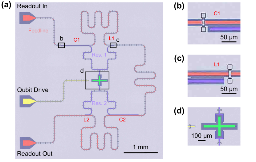
We experimentally realize an all-pass readout resonator. The chip micrograph is shown in Fig. 4a, corresponding to the circuit model in Fig. 3e. The identical resonators (blue) are coupled to the feedline (red) capacitively on the open end (Fig. 4b) and inductively on the shorted end (Fig. 4c). The claw design in Fig. 4d provides symmetric qubit-resonator coupling rate to a single-island flux-tunable transmon qubit (green) with global magnetic flux bias and dedicated drive line (yellow). We minimize sensitivity to spatial variation by making the two quarter-wave resonators geometrically identical and in very close proximity on the chip.
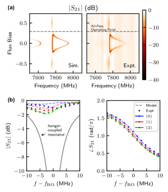
A 2D sweep of versus flux bias and frequency is shown in Fig. 5a. This tunable flux bias enables us to in situ tune the qubit-mediated coupling between the resonators, similar to the qubit-mediated coupling used for tunable couplers [28]. We observe that all-pass behavior occurs near the flux bias , corresponding to a dressed qubit frequency of , and choose this as our operating point. In Fig. 5a, we show excellent agreement with finite-element simulation, where the transmon qubit is approximated as a linear oscillator. See Appendix G for more details.
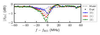
The measured magnitude and phase for the lowest three transmon states are shown in Fig. 5b. We calibrate the with respect to a through line that bypasses the package and wire-bonded chip. Based on the average away from the resonant point, we estimate insertion loss due to the package of in the frequency range of interest (see Appendix A). Adjusting for this package loss, the all-pass resonator’s transmission at the readout tone is above for the lowest three transmon states (see Table 2). The lowest dip in is .
| At readout tone | ||||
|---|---|---|---|---|
| Minimum of |
From the measured phase, we find a bare resonator frequency , resonator linewidth , and dispersive shift . From (11), we calculate a qubit-resonator coupling rate of .
In Fig. 5b, we overlay the analytic model for the full magnitude and phase of , where we include loss due to the package. The analytic model numerically solves the system Hamiltonian in (6) for the eigenmodes and and substitutes into the expression for in (4). Higher excited states of the transmon qubit and resonators are included to the point that the calculation converges. The linewidths of the system are given by and (see Appendix D). We use the analytic model to estimate the two remaining unknowns of the system, which are the phase delay and fixed resonator-resonator coupling rate . The even- and odd-mode linewidths are then and , in close agreement with our finite-element simulation (see Appendix G). In a future design, the linewidths could be matched by ensuring .
Without any Purcell suppression, the qubit’s Purcell decay rate would be given by , where the qubit is only coupled to the even mode. Unprotected, this would yield a Purcell-limited lifetime of . From finite-element simulation of the interference Purcell filter, we predict a Purcell suppression factor of . Indeed, we measure a prolonged qubit lifetime of that we predict to be limited by the drive line and intrinsic decay of the qubit. See Appendix G for further details.
V Single-Shot Readout
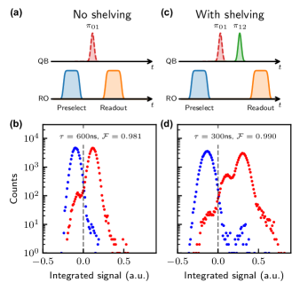
We demonstrate high-fidelity single-shot dispersive readout of the transmon qubit. We perform a standard readout pulse sequence (Fig. 6a). The readout pulse is implemented as a flat-top pulse with Gaussian rising and falling edges of width . We set the integration time to be the same as the duration that the readout pulse is at its maximum value. The pulse is implemented as a DRAG pulse [29] with . A Josephson traveling-wave parametric amplifier [4, 5] is used to amplify the output probe signal. A preselection pulse is included to only consider samples for which the qubit begins in the ground state. The preselection threshold is set at 99% of the fitted cumulative Gaussian distribution of the ground state [30].
Histograms of the amplified integrated quadratures are shown in Fig. 6b, where the qubit has been prepared in either or . We set the discrimination threshold at 0. We calculate the qubit readout assignment fidelity [31, 32], where is the probability that is measured given that was prepared. For integration time , we achieve readout fidelity of . We obtain an error of preparing a qubit in the ground state of . The error of preparing a qubit in the excited state is , where the error is dominated by qubit decay.
To assess the effect of a larger effective dispersive shift and longer qubit lifetime, we repeat this experiment with a shelving protocol (Fig. 6c), applying an unconditional pulse before the readout pulse [32]. A qubit in the first excited state is transferred to the second excited state, whereas a qubit in the ground state is unaffected. The pulse is also implemented as a DRAG pulse; the pulse parameters are optimized similarly to the standard method for the . The qubit is first prepared in , and Rabi experiments are performed to optimize pulse amplitude and frequency [32].
With this shelving protocol, the samples in the state are excited to the state, both increasing the dispersive shift from to and increasing the effective lifetime from to . This leads to an improved readout fidelity of with integration time , with and . The dominant error is still qubit decay, but as expected, the error has decreased due to the shorter integration time and longer effective lifetime. In the histogram in Fig. 6d, a “shoulder” representing the decay from the to the state is visible.
VI Conclusions
This work demonstrates the first all-pass readout of a superconducting qubit, where the readout resonator preferentially emits photons in one direction across its full bandwidth. By removing the need for intentional mismatch, this scheme aims to minimize the spread of resonator linewidths and remove the overhead associated with impedance matching. Moreover, the removal of intentional mismatch enables modular and flexible placement of resonator-qubit blocks along the feedline. This presents a path towards robust and scalable readout for large-scale quantum computers. We have developed a design for the all-pass readout of a transmon qubit and have demonstrated high-fidelity single-shot readout with all-pass performance.
To enable faster readout, further investigation is needed of all-pass resonator structures that operate in the regime where the dispersive shift is comparable to the resonator linewidth, without sacrificing directionality in either of the qubit’s computational states. Another future direction would be to investigate structures insensitive to local fabrication defects that could cause the bare resonator modes to be mismatched.
Due to the larger footprint, we expect that all-pass readout will be best suited for 3D integration such as a flip-chip geometry, where the qubits are on a separate chip from the readout and control lines [33]. The design could be compacted by using closer spacing between resonators, tighter meandering, and increased effective dielectric constant, the last of which is possible through 3D integration [33]. With these miniaturization efforts, future work could implement a multiplexed system using all-pass readout and empirically demonstrate lower variation of resonator linewidths.
Acknowledgements
The authors thank Neereja M. Sundaresan, Oliver E. Dial, and David W. Abraham for insightful discussions.
This work was supported in part by the MIT-IBM Watson AI Lab. This material is based upon work supported by the Under Secretary of Defense for Research and Engineering under Air Force Contract No. FA8702-15-D-0001. Any opinions, findings, conclusions or recommendations expressed in this material are those of the author(s) and do not necessarily reflect the views of the Under Secretary of Defense for Research and Engineering. A.Y. and J.W. acknowledge support from the NSF Graduate Research Fellowship. Y.Y. acknowledges support from the IBM PhD Fellowship and the NSERC Postgraduate Scholarship. G.C. acknowledges support from the Harvard Graduate School of Arts and Sciences Prize Fellowship.
A.Y. developed the theoretical framework, designed the device and experimental procedure, conducted the measurements, and analyzed the data. K.P.O. and A.Y. proposed the idea of all-pass readout. A.Y., Y.Y., K.P., J.W., and G.C. contributed to the experimental setup. M.G., B.M.N., and H.S. fabricated the device. A.Y. and K.P.O. designed the custom package and circuit board. A.Y., J.W., and K.P.O. developed the fabrication process for the custom circuit board. A.Y. packaged the device. K.S., M.E.S., and K.P.O. supervised the project. A.Y. wrote the manuscript with input from all co-authors. All authors contributed to the discussion of the results and the manuscript.
Appendix A Sample and Setup
| transition frequency | ||
|---|---|---|
| transition frequency | ||
| relaxation time | ||
| dephasing time | ||
| relaxation time | ||
| Flux bias | 0.291 | |
| Resonator frequency (bare) | ||
| Resonator linewidth | ||
| Resonator dispersive shifts { | ||
The transmon qubit and resonators are comprised of layers of thin-film aluminum on a silicon substrate. Airbridges are patterned to mitigate the formation of slot-line modes. The measured device parameters are listed in Table 3. We note that the reduced is expected, as we are far detuned from the flux-insensitive sweet spot at [34].
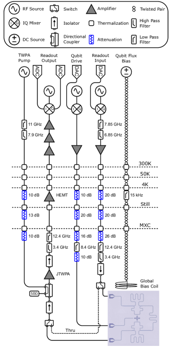
The diagram of the experimental setup is shown in Fig. 7. We conducted the experiment in a Bluefors LD400 dilution refrigerator with a base temperature of at the mixing chamber (MXC). The device is enclosed by a superconducting aluminum shield, which is nested within a Cryoperm shield mounted at the MXC. Microwave readout and drive tones are applied by a QICK ZCU111 RFSoC FPGA [35]. The sample is housed within a custom package that is designed to suppress modes below , which is more than sufficient for the experiment to avoid deleterious effects on qubit lifetime [36].
Appendix B Effective Linewidth in the Presence of Mismatches
Here, we derive the general expression for the effective linewidth of a single-mode resonator in the presence of mismatches at both ends of the feedline, using the input-output relations [37], also known as coupled mode theory [38]. Since the effective linewidth is a function of the standing waves in the feedline between the mismatches, it is dependent on the reflection coefficients and , which we capture by representative capacitances in this analysis. This derivation expands on that in [9], which calculated the linewidth of a resonant mode in the presence of capacitance on one end of the feedline.
We depict the input-output network in Fig. 9a. The evolution of the resonator mode is given by
| (12) |
The input-output relations of the resonator are governed by
| (13) |
with input () and output () directions shown in Fig. 9a.
The T-junction connecting the resonator to the feedline’s right () and left () sides is symmetric, reciprocal, and lossless. The scattering relations that satisfy this are [39, 9]
| (14) |
| (15) |
and
| (16) |
The input-side capacitance has the scattering relations [39]
| (17) |
and
| (18) |
Similarly, the output-side capacitance has the scattering relations
| (19) |
and
| (20) |
Eliminating the and modes, we obtain
| (21) |
Next, eliminating the and modes, we find
| (22) | ||||
We can then substitute into the original equation of motion in (12) to obtain
| (23) | ||||
where the effective frequency is
| (24) |
and the effective linewidth is
| (25) |
In the following sections, we use this general form to derive the expressions given in Sec. II.
B.1 Spread Due to Off-Chip Mismatch:
With Intentional Mismatch
We consider the special case where , representing intentional mismatch of total reflection with negligible dispersion. The effective linewidth in (25) simplifies to
| (26) |
We model as an off-chip mismatch positioned electrical length away with magnitude (see Fig. 9b). If the transmission line is lossless, then [39]. We now have
| (27) |
The ratio of the maximum () and minimum () linewidths simplifies to
| (28) |
B.2 Spread Due to Off-Chip Mismatch:
No Intentional Mismatch
B.3 Sensitivity to On-Chip Non-Uniformities:
With Intentional Mismatch
For a feedline with intentional mismatch, we derive the effect of non-uniformities on . For simplicity, we omit the effect of off-chip mismatches on the output side and set . We now have
| (32) |
We assume the resonator is spaced some distance away from the intentional mismatch (see Fig. 9d). The reflection coefficient of a lossless transmission line of length terminated in a mismatch with magnitude is given by [39]
| (33) |
where is the phase constant. In the case of intentional mismatch, . We now have
| (34) |
where we have denoted to represent the maximum possible linewidth. Assuming the readout tone is at the resonator frequency with wavelength , the phase constant along the feedline is given by
| (35) |
where {, } and {, } are the phase velocity and effective permittivity of the {feedline, resonator}. For simplicity, we have not included the effects of on . Substituting into (35), we have
| (36) |
Appendix C Amplifier Impedance Matching
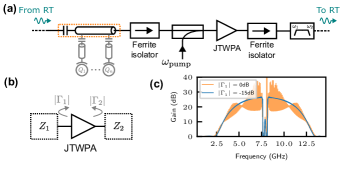
Here, we show that intentional mismatch adds to the overhead of multiplexed qubit readout by requiring nonreciprocal components to impedance match to downstream amplifiers [19, 20, 9, 21]. Contemporary quantum measurement chains use off-chip ferrite-based isolators biased by permanent magnets to realize wideband, unidirectional signal flow. While prevalent and essential for current experiments, these components act as a major inconvenience, since they dominate the available space at the base temperature stage and their high magnetic fields make integration with superconducting qubits infeasible. While significant research has investigated the integration of on-chip circulators [40, 41, 42, 21, 43, 44], no experimental devices with broad instantaneous bandwidth and sufficient isolation have yet been demonstrated.
We illustrate why amplifier impedance matching is needed by considering a typical quantum measurement chain, shown in Fig. 10a. Here, we use a Josephson traveling-wave parametric amplifier (JTWPA) for its broad bandwidth and high gain, which is suitable for multiplexed qubit readout [4, 5]. If not compensated, we show how impedance mismatch can create parametric oscillations in the JTWPA. The environment surrounding the amplifier can be represented by the circuit in Fig. 10b. We simulate the gain performance for different impedance environments using JosephsonCircuits.jl [45]. Our simulation uses a Floquet-mode JTWPA as the best-case scenario since it is inherently robust to out-of-band mismatch [20]. For the output side, we assume , representing the reflection from the isolator at the JTWPA’s output. For the input side, we use values of , characteristic of either the intentional mismatch or isolator at the input, respectively. From Fig. 10c, we see that proper matching on the input side (i.e., low ) strongly suppresses gain ripples, thus mitigating parametric oscillations and instability. We reiterate that this is a best-case analysis since the Floquet-mode JTWPA is robust to out-of-band mismatch.
The leading strategy of contemporary readout is to add an isolator before the JTWPA to compensate for the intentional mismatch. We propose that, alternatively, one could instead make the quantum processor better impedance-matched by design by removing this mismatch. This would reduce the need for isolation before the JTWPA; however, we note that isolation from the pump tone and amplified vacuum fluctuations would still be needed. Nevertheless, removing the feedline mismatch would be a major step toward the monolithic integration of qubits and quantum-limited amplifiers. Such integration would both drastically reduce the footprint of the external microwave infrastructure and mitigate preamplification losses.
Appendix D Input-Output Theory of All-Pass Readout
This appendix derives the expression in (4) for a resonator with an even and odd mode, again using the coupled mode equations [38]. We also show the equivalence of the generalized system with the two-resonator system.
First, we consider a generalized resonator with an even and odd mode with amplitudes and , respectively, as in Fig. 11a. For such modes, we expect that forward and backward propagating waves would couple in phase to the symmetric mode and out of phase to the antisymmetric mode. We can determine the mode evolution as [23]
| (37) |
and
| (38) |
The input-output equations are given by
| (39) |
and
| (40) |
Letting , we can solve for the transmission as
| (41) |
If the modes are degenerate, then they have equal frequencies and equal linewidths, i.e.,
| (42) |
and
| (43) |
Eq. (41) then becomes
| (44) |
This is the desired all-pass behavior, since we have at .
Now, we consider our system, as shown in Fig. 11b. We approximate the weakly anharmonic transmon qubit as a linear oscillator. This analysis derives the waveguide-mediated coupling and matching condition but will omit the nonlinear correction for and . See Appendix E for the calculation of and with the nonlinear correction. From coupled-mode theory [38], the evolution of the modes is given by
| (45) | ||||
| (46) | ||||
and
| (47) |
where , is the propagation constant, and is the separation between the resonators.
Assuming dependence, we can solve for a steady-state expression for the qubit mode , where (47) becomes
| (48) |
Noting that the qubit mode mediates a coupling at , we substitute (48) into (45) and (46), and obtain
| (49) | ||||
Defining the even and odd modes as
| (50) |
we can derive the evolution of the even and odd modes (without nonlinear correction) analogous to (37) and (38) as
| (51) | ||||
where
| (52) |
| (53) |
and
| (54) |
The waveguide-mediated coupling is thus given by . To match the linewidths of the even and odd modes , we require the electrical length to satisfy .
Appendix E Hamiltonian of All-Pass Readout
This appendix derives the Hamiltonian for the circuit in Fig. 11c. The Hamiltonian for two resonators coupled symmetrically to a qubit in the transmon regime is approximated in the Fock basis by
| (55) | ||||
We now transform the basis to normal, diagonalized modes of the system. Since the resonators are symmetrically coupled to the qubit, we can transform to an even and odd basis by the transformation in (50), which is equivalently,
| (56) |
Applying the rotating wave approximation to (55) and substituting the transformation from (56), we obtain
| (57) | ||||
Only the last term needs to be diagonalized. Assuming this interaction term is small relative to the detuning, we can perform a standard Schrieffer-Wolff transformation [46], truncate to the first two levels, and derive the Hamiltonian in the dispersive limit as
| (58) |
where the dressed qubit frequency , even mode frequency , odd mode frequency , and effective dispersive shift are given by
| (59) |
| (60) |
| (61) |
and
| (62) |
where the qubit-resonator detuning is .
Appendix F Scaling of
Due to the qubit’s nonlinearity, the degeneracy of our system will be disrupted depending on the qubit state. Here, we discuss how the transmission of this form of all-pass readout is expected to scale with . We assume the case in which so that the even and odd modes are roughly equal . We denote the dressed resonator mode as . In this case, from (60) and (61), we obtain
| (63) |
and
| (64) |
We also assume a lossless feedline and that the even and odd modes have equal linewidths . We substitute into (41) and have
| (65) | ||||
The maximum difference in phase between the two states occurs for a readout tone positioned at . The transmission at this frequency is given by
| (66) |
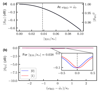
The magnitude is the same for both the ground and excited states and is plotted versus in Fig. 12a. The proportion of measurement photons decaying towards the output is characterized by . Targeting large , we operate at , denoted by the vertical dashed line. For this parameter choice, we plot the analytic versus in Fig. 12b.
Appendix G Finite-Element Simulation
We predict the performance of our device using finite-element method (FEM) simulation in Ansys High Frequency Simulation Software (HFSS). We first fine-tune the permittivity to match the measured resonator frequency. We model our system as a 3-port device, where ports 1 and 2 are the readout input and output, respectively, and port 3 replaces the Josephson junction.
If we approximate the transmon qubit as a linear oscillator, we can calculate the qubit’s external coupling to the waveguide as [47]
| (67) |
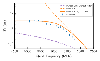
where is the input admittance from the perspective of the Josephson junction and is the total capacitance of the transmon. We simulate the admittance parameters of this 3-port system, calculate the input admittance looking into port 3, and substitute into (67). The simulated Purcell-limited lifetime of the design with interference Purcell filter is shown in Fig. 13. At our operating point (denoted by the gray vertical line), the Purcell-limited lifetime is , corresponding to a Purcell suppression factor of . With further optimization, it has been experimentally demonstrated that interference Purcell suppression exceeding 2 orders of magnitude over several hundred megahertz is possible [22].
As shown in Fig. 5a, we obtain strong agreement between simulated and experimental as a function of the flux biasing the superconducting quantum interference device (SQUID) of the flux-tunable transmon. Approximating the transmon qubit as a linear oscillator, we terminate port 3 with an inductor and simulate . We sweep the inductance according to the Josephson inductance of a symmetric SQUID given by , where [46] with fitted .
Finally, we terminate both ports 1 and 2 with and perform eigenmode simulation to predict the linewidths of the two resonator modes of our system. Assuming the qubit is far detuned from the resonators, we predict linewidths of and , in close agreement with the experimental fits of and .
References
- Blais et al. [2004] A. Blais, R.-S. Huang, A. Wallraff, S. M. Girvin, and R. J. Schoelkopf, Cavity quantum electrodynamics for superconducting electrical circuits: An architecture for quantum computation, Physical Review A 69, 062320 (2004).
- Schuster et al. [2005] D. I. Schuster, A. Wallraff, A. Blais, L. Frunzio, R.-S. Huang, J. Majer, S. M. Girvin, and R. J. Schoelkopf, Ac Stark Shift and Dephasing of a Superconducting Qubit Strongly Coupled to a Cavity Field, Physical Review Letters 94, 123602 (2005).
- Gambetta et al. [2006] J. Gambetta, A. Blais, D. I. Schuster, A. Wallraff, L. Frunzio, J. Majer, M. H. Devoret, S. M. Girvin, and R. J. Schoelkopf, Qubit-photon interactions in a cavity: Measurement-induced dephasing and number splitting, Physical Review A 74, 042318 (2006).
- Macklin et al. [2015] C. Macklin, K. O’Brien, D. Hover, M. E. Schwartz, V. Bolkhovsky, X. Zhang, W. D. Oliver, and I. Siddiqi, A near-quantum-limited Josephson traveling-wave parametric amplifier, Science 350, 307 (2015).
- O’Brien et al. [2014] K. O’Brien, C. Macklin, I. Siddiqi, and X. Zhang, Resonant Phase Matching of Josephson Junction Traveling Wave Parametric Amplifiers, Physical Review Letters 113, 157001 (2014).
- Reed et al. [2010] M. D. Reed, B. R. Johnson, A. A. Houck, L. DiCarlo, J. M. Chow, D. I. Schuster, L. Frunzio, and R. J. Schoelkopf, Fast reset and suppressing spontaneous emission of a superconducting qubit, Applied Physics Letters 96, 203110 (2010).
- Sete et al. [2015] E. A. Sete, J. M. Martinis, and A. N. Korotkov, Quantum theory of a bandpass Purcell filter for qubit readout, Physical Review A 92, 012325 (2015).
- Jeffrey et al. [2014] E. Jeffrey, D. Sank, J. Y. Mutus, T. C. White, J. Kelly, R. Barends, Y. Chen, Z. Chen, B. Chiaro, A. Dunsworth, A. Megrant, P. J. J. O’Malley, C. Neill, P. Roushan, A. Vainsencher, J. Wenner, A. N. Cleland, and J. M. Martinis, Fast Accurate State Measurement with Superconducting Qubits, Physical Review Letters 112, 190504 (2014).
- Heinsoo et al. [2018] J. Heinsoo, C. K. Andersen, A. Remm, S. Krinner, T. Walter, Y. Salathé, S. Gasparinetti, J.-C. Besse, A. Potočnik, A. Wallraff, and C. Eichler, Rapid High-fidelity Multiplexed Readout of Superconducting Qubits, Physical Review Applied 10, 034040 (2018).
- Krinner et al. [2022] S. Krinner, N. Lacroix, A. Remm, A. Di Paolo, E. Genois, C. Leroux, C. Hellings, S. Lazar, F. Swiadek, J. Herrmann, G. J. Norris, C. K. Andersen, M. Müller, A. Blais, C. Eichler, and A. Wallraff, Realizing repeated quantum error correction in a distance-three surface code, Nature 605, 669 (2022).
- Google Quantum AI [2023] Google Quantum AI, Suppressing quantum errors by scaling a surface code logical qubit, Nature 614, 676 (2023).
- Google Quantum AI [2021] Google Quantum AI, Exponential suppression of bit or phase errors with cyclic error correction, Nature 595, 383 (2021).
- Sank et al. [2024] D. Sank, A. Opremcak, A. Bengtsson, M. Khezri, Z. Chen, O. Naaman, and A. Korotkov, System Characterization of Dispersive Readout in Superconducting Qubits (2024), arxiv:2402.00413 [quant-ph] .
- Bengtsson et al. [2024] A. Bengtsson, A. Opremcak, M. Khezri, D. Sank, A. Bourassa, K. J. Satzinger, S. Hong, C. Erickson, B. J. Lester, K. C. Miao, A. N. Korotkov, J. Kelly, Z. Chen, and P. V. Klimov, Model-based Optimization of Superconducting Qubit Readout (2024), arxiv:2308.02079 [cond-mat, physics:quant-ph] .
- Li et al. [2023] H.-X. Li, D. Shiri, S. Kosen, M. Rommel, L. Chayanun, A. Nylander, R. Rehammar, G. Tancredi, M. Caputo, K. Grigoras, L. Grönberg, J. Govenius, and J. Bylander, Experimentally Verified, Fast Analytic, and Numerical Design of Superconducting Resonators in Flip-Chip Architectures, IEEE Transactions on Quantum Engineering 4, 1 (2023).
- Chow et al. [2015] J. M. Chow, S. J. Srinivasan, E. Magesan, A. D. Córcoles, D. W. Abraham, J. M. Gambetta, and M. Steffen, Characterizing a four-qubit planar lattice for arbitrary error detection, in SPIE Sensing Technology + Applications (Baltimore, Maryland, United States, 2015) p. 95001G.
- Clerk et al. [2010] A. A. Clerk, M. H. Devoret, S. M. Girvin, F. Marquardt, and R. J. Schoelkopf, Introduction to Quantum Noise, Measurement and Amplification, Reviews of Modern Physics 82, 1155 (2010), arxiv:0810.4729 .
- Kosen et al. [2022] S. Kosen, H.-X. Li, M. Rommel, D. Shiri, C. Warren, L. Grönberg, J. Salonen, T. Abad, J. Biznárová, M. Caputo, L. Chen, K. Grigoras, G. Johansson, A. F. Kockum, C. Križan, D. P. Lozano, G. J. Norris, A. Osman, J. Fernández-Pendás, A. Ronzani, A. F. Roudsari, S. Simbierowicz, G. Tancredi, A. Wallraff, C. Eichler, J. Govenius, and J. Bylander, Building blocks of a flip-chip integrated superconducting quantum processor, Quantum Science and Technology 7, 035018 (2022).
- Peng et al. [2022a] K. Peng, R. Poore, P. Krantz, D. E. Root, and K. P. O’Brien, X-parameter based design and simulation of Josephson traveling-wave parametric amplifiers for quantum computing applications, in 2022 IEEE International Conference on Quantum Computing and Engineering (QCE) (IEEE, Broomfield, CO, USA, 2022) pp. 331–340.
- Peng et al. [2022b] K. Peng, M. Naghiloo, J. Wang, G. D. Cunningham, Y. Ye, and K. P. O’Brien, Floquet-Mode Traveling-Wave Parametric Amplifiers, PRX Quantum 3, 020306 (2022b).
- Ranzani and Aumentado [2019] L. Ranzani and J. Aumentado, Circulators at the Quantum Limit: Recent Realizations of Quantum-Limited Superconducting Circulators and Related Approaches, IEEE Microwave Magazine 20, 112 (2019).
- [22] A. Yen, Y. Ye, K. Peng, J. Wang, G. Cunningham, M. Gingras, B. M. Niedzielski, H. Stickler, K. Serniak, M. E. Schwartz, and K. P. O’Brien, Interference Purcell Suppression of a Superconducting Qubit (In Preparation).
- Manolatou et al. [1999] C. Manolatou, M. Khan, S. Fan, P. Villeneuve, H. Haus, and J. Joannopoulos, Coupling of modes analysis of resonant channel add-drop filters, IEEE Journal of Quantum Electronics 35, 1322 (1999).
- Gheeraert et al. [2020] N. Gheeraert, S. Kono, and Y. Nakamura, Programmable directional emitter and receiver of itinerant microwave photons in a waveguide, Physical Review A 102, 053720 (2020).
- Kannan et al. [2023] B. Kannan, A. Almanakly, Y. Sung, A. Di Paolo, D. A. Rower, J. Braumüller, A. Melville, B. M. Niedzielski, A. Karamlou, K. Serniak, A. Vepsäläinen, M. E. Schwartz, J. L. Yoder, R. Winik, J. I.-J. Wang, T. P. Orlando, S. Gustavsson, J. A. Grover, and W. D. Oliver, On-demand directional microwave photon emission using waveguide quantum electrodynamics, Nature Physics 19, 394 (2023).
- Kockum et al. [2018] A. F. Kockum, G. Johansson, and F. Nori, Decoherence-Free Interaction between Giant Atoms in Waveguide Quantum Electrodynamics, Physical Review Letters 120, 140404 (2018).
- Kannan et al. [2020] B. Kannan, M. J. Ruckriegel, D. L. Campbell, A. Frisk Kockum, J. Braumüller, D. K. Kim, M. Kjaergaard, P. Krantz, A. Melville, B. M. Niedzielski, A. Vepsäläinen, R. Winik, J. L. Yoder, F. Nori, T. P. Orlando, S. Gustavsson, and W. D. Oliver, Waveguide quantum electrodynamics with superconducting artificial giant atoms, Nature 583, 775 (2020).
- Yan et al. [2018] F. Yan, P. Krantz, Y. Sung, M. Kjaergaard, D. L. Campbell, T. P. Orlando, S. Gustavsson, and W. D. Oliver, Tunable Coupling Scheme for Implementing High-Fidelity Two-Qubit Gates, Physical Review Applied 10, 054062 (2018).
- Motzoi et al. [2009] F. Motzoi, J. M. Gambetta, P. Rebentrost, and F. K. Wilhelm, Simple Pulses for Elimination of Leakage in Weakly Nonlinear Qubits, Physical Review Letters 103, 110501 (2009).
- Walter et al. [2017] T. Walter, P. Kurpiers, S. Gasparinetti, P. Magnard, A. Potočnik, Y. Salathé, M. Pechal, M. Mondal, M. Oppliger, C. Eichler, and A. Wallraff, Rapid High-Fidelity Single-Shot Dispersive Readout of Superconducting Qubits, Physical Review Applied 7, 054020 (2017).
- Sunada et al. [2022] Y. Sunada, S. Kono, J. Ilves, S. Tamate, T. Sugiyama, Y. Tabuchi, and Y. Nakamura, Fast Readout and Reset of a Superconducting Qubit Coupled to a Resonator with an Intrinsic Purcell Filter, Physical Review Applied 17, 044016 (2022).
- Chen et al. [2023] L. Chen, H.-X. Li, Y. Lu, C. W. Warren, C. J. Križan, S. Kosen, M. Rommel, S. Ahmed, A. Osman, J. Biznárová, A. Fadavi Roudsari, B. Lienhard, M. Caputo, K. Grigoras, L. Grönberg, J. Govenius, A. F. Kockum, P. Delsing, J. Bylander, and G. Tancredi, Transmon qubit readout fidelity at the threshold for quantum error correction without a quantum-limited amplifier, npj Quantum Information 9, 1 (2023).
- Rosenberg et al. [2017] D. Rosenberg, D. Kim, R. Das, D. Yost, S. Gustavsson, D. Hover, P. Krantz, A. Melville, L. Racz, G. O. Samach, S. J. Weber, F. Yan, J. L. Yoder, A. J. Kerman, and W. D. Oliver, 3D integrated superconducting qubits, npj Quantum Information 3, 1 (2017).
- Koch et al. [2007] J. Koch, T. M. Yu, J. Gambetta, A. A. Houck, D. I. Schuster, J. Majer, A. Blais, M. H. Devoret, S. M. Girvin, and R. J. Schoelkopf, Charge-insensitive qubit design derived from the Cooper pair box, Physical Review A 76, 042319 (2007).
- Stefanazzi et al. [2022] L. Stefanazzi, K. Treptow, N. Wilcer, C. Stoughton, C. Bradford, S. Uemura, S. Zorzetti, S. Montella, G. Cancelo, S. Sussman, A. Houck, S. Saxena, H. Arnaldi, A. Agrawal, H. Zhang, C. Ding, and D. I. Schuster, The QICK (Quantum Instrumentation Control Kit): Readout and control for qubits and detectors, Review of Scientific Instruments 93, 044709 (2022).
- Huang et al. [2021] S. Huang, B. Lienhard, G. Calusine, A. Vepsäläinen, J. Braumüller, D. K. Kim, A. J. Melville, B. M. Niedzielski, J. L. Yoder, B. Kannan, T. P. Orlando, S. Gustavsson, and W. D. Oliver, Microwave Package Design for Superconducting Quantum Processors, PRX Quantum 2, 020306 (2021).
- Gardiner and Collett [1985] C. W. Gardiner and M. J. Collett, Input and output in damped quantum systems: Quantum stochastic differential equations and the master equation, Physical Review A 31, 3761 (1985).
- Haus [1984] H. A. Haus, Waves and Fields in Optoelectronics, Prentice-Hall Series in Solid State Physical Electronics (Prentice-Hall, Englewood Cliffs, NJ, 1984).
- Pozar [2012] D. M. Pozar, Microwave Engineering, 4th ed. (Wiley, Hoboken, NJ, 2012).
- Kamal et al. [2011] A. Kamal, J. Clarke, and M. H. Devoret, Noiseless non-reciprocity in a parametric active device, Nature Physics 7, 311 (2011).
- Chapman et al. [2017] B. J. Chapman, E. I. Rosenthal, J. Kerckhoff, B. A. Moores, L. R. Vale, J. A. B. Mates, G. C. Hilton, K. Lalumière, A. Blais, and K. W. Lehnert, Widely Tunable On-Chip Microwave Circulator for Superconducting Quantum Circuits, Physical Review X 7, 041043 (2017).
- Chapman et al. [2019] B. J. Chapman, E. I. Rosenthal, and K. W. Lehnert, Design of an On-Chip Superconducting Microwave Circulator with Octave Bandwidth, Physical Review Applied 11, 044048 (2019).
- Kerckhoff et al. [2015] J. Kerckhoff, K. Lalumière, B. J. Chapman, A. Blais, and K. W. Lehnert, On-Chip Superconducting Microwave Circulator from Synthetic Rotation, Physical Review Applied 4, 034002 (2015).
- Sliwa et al. [2015] K. M. Sliwa, M. Hatridge, A. Narla, S. Shankar, L. Frunzio, R. J. Schoelkopf, and M. H. Devoret, Reconfigurable Josephson Circulator/Directional Amplifier, Physical Review X 5, 041020 (2015).
- O’Brien [2024] K. P. O’Brien, JosephsonCircuits.jl (2024).
- Blais et al. [2021] A. Blais, A. L. Grimsmo, S. M. Girvin, and A. Wallraff, Circuit Quantum Electrodynamics, Reviews of Modern Physics 93, 025005 (2021).
- Esteve et al. [1986] D. Esteve, M. H. Devoret, and J. M. Martinis, Effect of an arbitrary dissipative circuit on the quantum energy levels and tunneling of a Josephson junction, Physical Review B 34, 158 (1986).