Spatial Variation-Aware Read Disturbance Defenses:
Experimental Analysis of Real DRAM Chips
and Implications on Future Solutions
Abstract
Read disturbance in modern DRAM chips is a widespread phenomenon and is reliably used for breaking memory isolation, a fundamental building block for building robust systems. RowHammer and RowPress are two examples of read disturbance in DRAM where repeatedly accessing (hammering) or keeping active (pressing) a memory location induces bitflips in other memory locations. Unfortunately, shrinking technology node size exacerbates read disturbance in DRAM chips over generations. As a result, existing defense mechanisms suffer from significant performance and energy overheads, limited effectiveness, or prohibitively high hardware complexity.
In this paper, we tackle these shortcomings by leveraging the spatial variation in read disturbance across different memory locations in real DRAM chips. To do so, we 1) present the first rigorous real DRAM chip characterization study of spatial variation of read disturbance and 2) propose Svärd, a new mechanism that dynamically adapts the aggressiveness of existing solutions based on the row-level read disturbance profile. Our experimental characterization on 144 real DDR4 DRAM chips representing 10 chip designs demonstrates a large variation in read disturbance vulnerability across different memory locations: in the part of memory with the worst read disturbance vulnerability, 1) up to the number of bitflips can occur and 2) bitflips can occur at an order of magnitude fewer accesses, compared to the memory locations with the least vulnerability to read disturbance. Svärd leverages this variation to reduce the overheads of five state-of-the-art read disturbance solutions, and thus significantly increases system performance.
1 Introduction
To ensure system robustness (including reliability, security, and safety), it is critical to maintain memory isolation: accessing a memory address should not cause unintended side-effects on data stored on other addresses [1]. Unfortunately, with aggressive technology scaling, DRAM [2], the prevalent main memory technology, suffers from increased read disturbance: accessing (reading) a row of DRAM cells (i.e., a DRAM row) degrades the data integrity of other physically close but unaccessed DRAM rows. RowHammer and RowPress are two prime examples of the DRAM read disturbance phenomenon where a DRAM row (i.e., victim row) can experience bitflips when a nearby DRAM row (i.e., aggressor row) is 1) repeatedly opened (i.e., hammered) [3, 4, 5, 6, 7, 8, 9, 10, 1, 11, 12, 13, 14, 15, 16, 17, 18, 19, 20, 21, 22, 23, 24, 25, 26, 27, 28, 29, 30, 31, 32, 33, 34, 35, 36, 37, 38, 39, 40, 41, 42, 43, 44, 45, 46, 47, 48, 49, 50, 51, 52, 53, 54, 55, 56, 57, 58, 59, 60, 61, 62, 63, 64, 65, 66, 67, 68, 69] or 2) kept open for a long period (i.e., pressed) [70], respectively.
Many prior works demonstrate attacks on a wide range of systems that exploit read disturbance to escalate privilege, leak private data, and manipulate critical application outputs [3, 4, 5, 6, 7, 8, 9, 10, 1, 11, 12, 13, 14, 15, 16, 17, 18, 19, 20, 21, 22, 23, 24, 25, 26, 27, 28, 29, 30, 31, 32, 33, 34, 35, 36, 37, 38, 39, 40, 41, 42, 43, 44, 45, 46, 47, 48, 49, 50, 51, 52, 53, 71, 72, 73, 74, 75, 76, 77, 78, 79, 80, 81, 82, 83, 84]. To make matters worse, various experimental studies [1, 25, 33, 36, 37, 61, 1, 70] find that newer DRAM chip generations are more susceptible to read disturbance. For example, chips manufactured in 2018-2020 can experience RowHammer bitflips at an order of magnitude fewer row activations compared to the chips manufactured in 2012-2013 [61]. As read disturbance in DRAM chips worsens, ensuring robust (i.e., reliable, secure, and safe) operation becomes more expensive in terms of performance overhead, energy consumption, and hardware complexity [61, 85, 86]. Therefore, it is critical to understand the read disturbance vulnerabilities of DRAM chips in greater detail with in-depth insights in order to develop more effective and efficient solutions for current and future DRAM-based memory systems. To this end, prior works study various characteristics of DRAM read disturbance [87, 1, 88, 54, 89, 55, 56, 57, 90, 91, 58, 59, 92, 60, 61, 62, 93, 46, 49, 63, 64, 65, 66, 67, 68, 69, 94, 95, 36, 25, 96, 33, 97, 98, 99, 70]. Unfortunately, no prior work rigorously studies the spatial variation of DRAM read disturbance and its implications on future solutions.
Our goal in this paper is to build a detailed understanding of the spatial variation in read disturbance across DRAM rows and leverage this understanding to improve the existing solutions. To this end, in this paper, we 1) present the first rigorous experimental characterization of the spatial variation in read disturbance vulnerabilities of real DRAM chips, and 2) propose Svärd, a new mechanism that dynamically adapts the aggressiveness of existing solutions based on the observed variation.
Characterization. We test 144 modern real DDR4 DRAM chips representing 10 different chip designs from three major manufacturers.111We test DRAM chips from Samsung, SK Hynix, and Micron, which hold the largest market shares of 40.7%, 28.8%, and 26.4% respectively [100, 101]. Chip design is identified by chip density, die revision, and chip organization. Our experimental results show that the read disturbance vulnerabilities of DRAM chips vary significantly and irregularly across 1) DRAM rows within a DRAM subarray, i.e., a two-dimensional DRAM array that consists of hundreds of DRAM rows (§2) and 2) subarrays within a DRAM bank, i.e., a group of many subarrays that share an I/O circuitry (§2). We make two key observations from our characterization: 1) the fraction of erroneous DRAM cells, i.e., bit error rate (), varies by a factor of and 2) the minimum hammer count required to induce the first bitflip () varies by an order of magnitude across DRAM rows in a subarray.
We investigate the correlations between a victim DRAM row’s spatial features (i.e., physical location within the corresponding subarray and bank) and read disturbance vulnerability in two steps. First, we reverse engineer the organization of a DRAM bank. Second, we perform extensive statistical analyses based on 1) reverse-engineered spatial features and 2) observed values. We make the key observation that the variation in read disturbance vulnerability across DRAM rows correlates well with the spatial features of DRAM rows only in four out of 15 tested DRAM modules. Therefore, we conclude that read disturbance vulnerability irregularly varies across DRAM rows, and thus, row-level spatial features we evaluate are insufficient to predict read disturbance vulnerability.
Improving existing solutions. Based on the understanding we develop via our rigorous experimental characterization, we propose Svärd, a new mechanism that dynamically adapts the aggressiveness of existing solutions to the read disturbance vulnerability level of each potential victim row. Svärd forces an existing solution to react more aggressively to an aggressor row activation (e.g., preventively refresh the potential victim row) if a potential victim row is more vulnerable to read disturbance. Svärd is implemented together with existing solutions, which can be either 1) in the memory controller within the processor chip (i.e., without modifications to the DRAM chip or DRAM interface) or 2) within the DRAM chip (i.e., transparent to the rest of the system). We evaluate the performance benefits of Svärd on five state-of-the-art solutions, AQUA [102], BlockHammer [85], Hydra [103], PARA [1], and RRS [104] using three representative spatial distribution profiles of read disturbance that we generate based on our experimental characterization of real DRAM chips (i.e., one for each manufacturer). Our performance evaluation results show that Svärd significantly reduces the performance overheads of AQUA, BlockHammer, Hydra, PARA, and RRS, leading to system performance improvements of , , , , and , respectively, on average across 120 multiprogrammed memory-intensive workloads.
We make the following contributions:
-
•
We present the first rigorous characterization of the spatial variation of read disturbance in modern DRAM chips. Our experimental results on 144 real DDR4 DRAM chips spanning 10 different chip designs show a significant and irregular variation in read disturbance vulnerability across DRAM rows.
-
•
We propose Svärd, a new mechanism that dynamically adapts the aggressiveness of an existing read disturbance solution to the vulnerability level of the potential victim row.
-
•
We showcase Svärd’s integration with five different state-of-the-art read disturbance solutions. Our results show that Svärd reduces the performance overhead of these four state-of-the-art solutions, leading to large system performance benefits.
2 Background
This section provides a concise overview of 1) DRAM organization and operation and 2) DRAM read disturbance. For more detail, we refer the reader to prior works on DRAM and read disturbance [105, 106, 107, 108, 109, 110, 111, 112, 113, 114, 115, 116, 1, 117, 118, 119, 120, 121, 122, 61, 123, 36, 124, 125, 126, 127, 128, 129, 130, 131, 132, 133, 134, 135, 136, 137, 138, 139, 140, 141, 142].
2.1 DRAM Organization and Operation
Organization. Fig. 1a shows the organization of DRAM-based memory systems. A memory channel connects the processor (CPU) to a set of DRAM chips, called DRAM rank. Chips in a DRAM rank operate in lock-step. Each chip has multiple DRAM banks, each consisting of multiple DRAM cell arrays (called subarrays) and their local I/O circuitry. Within a subarray, DRAM cells are organized as a two-dimensional array of DRAM rows and columns. A DRAM cell stores one bit of data in the form of electrical charge in a capacitor, which can be accessed through an access transistor. A wire called wordline drives the gate of all DRAM cells’ access transistors in a DRAM row. A wire called bitline connects all DRAM cells in a DRAM column to a common differential sense amplifier. Therefore, when a wordline is asserted, each DRAM cell in the DRAM row is connected to its corresponding sense amplifier. The set of sense amplifiers in a subarray is called the row buffer, where the data of an activated DRAM row is buffered to serve a column access.
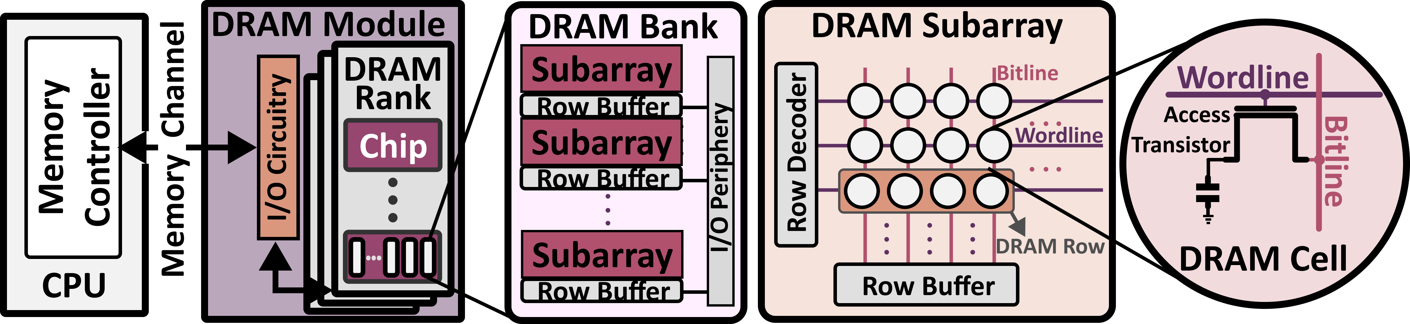
Operation. The memory controller serves memory access requests by issuing DRAM commands, e.g., row activation (), bank precharge (), data read (), data write (), and refresh () while respecting certain timing parameters to guarantee correct operation [143, 144, 145, 146, 147, 148, 149]. To read or write data; the memory controller first needs to activate the corresponding row. To do so, it issues an command alongside the bank address and row address corresponding to the memory request’s address. When a row is activated, its data is copied to and temporarily stored at the row buffer. The latency from the start of a row activation until the data is reliably readable/writable in the row buffer is called the row activation latency (). During the row activation process, a DRAM cell loses its charge, and thus, its initial charge needs to be restored (via a process called charge restoration). The latency from the start of a row activation until the completion of the DRAM cell’s charge restoration is called the charge restoration latency (). The memory controller can read/write data from/to the row buffer using / commands. The changes are propagated to the DRAM cells in the open row. Subsequent accesses to the same row can be served quickly from the row buffer (i.e., called a row hit) without issuing another to the same row. The latency of performing a read/write operation is called column access latency ()/column write latency (). To access another row in an already activated DRAM bank, the memory controller must issue a command to close the opened row and prepare the bank for a new activation. When the command is issued, the DRAM chip de-asserts the active row’s wordline and precharges the bitlines. The timing parameter for precharge is called the precharge latency ().
A DRAM cell is inherently leaky and thus loses its stored electrical charge over time. To maintain data integrity, a DRAM cell is periodically refreshed with a time interval called the , which is typically (e.g., [149, 148, 150]) or (e.g., [145, 143, 144]) at normal operating temperature (i.e., up to ) and half of it for the extended temperature range (i.e., above up to ). To timely refresh all cells, the memory controller periodically issues a refresh () command with a time interval called the refresh interval (), which is typically (e.g., [149, 148, 150]) or (e.g., [145, 143, 144]) at normal operating temperature. When a rank-/bank-level refresh command is issued, the DRAM chip internally refreshes several DRAM rows, during which the whole rank/bank is busy. This operation’s latency is called the refresh latency ().
2.2 Read Disturbance in DRAM
Read disturbance is the phenomenon that reading data from a memory or storage device causes physical disturbance (e.g., voltage deviation, electron injection, electron trapping) on another piece of data that is not accessed but physically located nearby the accessed data. Two prime examples of read disturbance in modern DRAM chips are RowHammer [1], and RowPress [70], where repeatedly accessing (hammering) or keeping active (pressing) a DRAM row induces bitflips in physically nearby DRAM rows, respectively. In RowHammer and RowPress terminology, the row that is hammered or pressed is called the aggressor row, and the row that experiences bitflips the victim row. For read disturbance bitflips to occur, 1) the aggressor row needs to be activated more than a certain threshold value, defined as [61] and/or 2) the time that an aggressor row stays active () [70] need to be large-enough [61, 62, 63, 70]. To avoid read disturbance bitflips, systems take preventive actions, e.g., they refresh victim rows [151, 152, 153, 154, 155, 156, 157, 158, 159, 160, 161, 86, 162, 163, 164, 165, 166, 167, 168, 1, 169, 170, 171, 36, 42, 172, 103, 173, 174, 175, 176, 177, 178, 179, 180, 181, 182], selectively throttle accesses to aggressor rows [85, 183], and physically isolate potential aggressor and victim rows [123, 184, 104, 102, 185, 186]. These solutions aim to perform preventive actions before the cumulative effect of an aggressor row’s activation count and on time causes read disturbance bitflips.
3 Motivation and Goal
Prior research experimentally demonstrates that read disturbance is clearly a worsening DRAM robustness (i.e., reliability, security, and safety) concern [1, 61, 36, 63, 62, 25, 96, 33, 37, 69, 70]. Despite all efforts, newer DRAM chips are shown to be significantly more vulnerable to read disturbance than older generations [61]. Even DRAM chips that have been marketed as RowHammer-free in 2018-2020 experience RowHammer bitflips at significantly lower hammer counts (e.g., 4.8K activations for each of two aggressor rows for LPDDR4 chips when target row refresh (TRR) protection222DRAM manufacturers implement RowHammer solutions, generally called Target Row Refresh (TRR) [36, 146, 148], which perform proprietary operations within DRAM to prevent RowHammer bitflips. is disabled [61] and 25K for DDR4 chips when TRR protection is enabled [36]) compared to the DDR3 DRAM chips manufactured in 2012-2013 (e.g., 139K [1] or 69K [61]). Many prior works [168, 152, 151, 183, 1, 163, 154, 153, 148, 187, 167, 155, 164, 165, 166, 188, 89, 169, 160, 159, 57, 90, 170, 156, 86, 171, 85, 36, 161, 42, 103, 104, 22, 184, 29, 158, 123, 92, 162, 189, 175, 176, 177, 190, 178, 102, 191, 192, 193, 182, 194, 195, 172, 173, 196, 197, 198, 179, 199, 200, 201, 69, 202, 203, 204, 186, 205, 185, 206, 207, 208, 84, 209, 210, 211, 212, 83, 213, 214, 180, 181] propose RowHammer solutions to provide RowHammer-safe operation with either probabilistic or deterministic security guarantees. Unfortunately, recent works [61, 85, 86, 25, 96, 33, 69, 42] demonstrate that many of these solutions will incur significant performance, energy consumption, and hardware complexity overheads such that they become prohibitively expensive when deployed in future DRAM chips with much larger read disturbance vulnerabilities [61].
To avoid read disturbance bitflips in future DRAM-based computing systems in an effective and efficient way, it is critical to rigorously gain detailed insights into the read disturbance phenomena under various circumstances (e.g., the physical location of the victim row in a DRAM chip). Although it might not be in the best interest of a DRAM manufacturer to make such understanding publicly available,333See [215] for a discussion and analysis of such issues. rigorous research in the public domain should continue to enable a much more detailed and rigorous understanding of DRAM read disturbance. This is important because a better understanding of DRAM read disturbance among the broader research community enables the development of comprehensive solutions to the problem more quickly. Unfortunately, despite the existing research efforts expended towards understanding read disturbance [87, 1, 88, 54, 89, 55, 56, 57, 90, 91, 58, 59, 92, 60, 61, 62, 93, 46, 49, 63, 64, 65, 66, 67, 68, 69, 94, 95, 36, 25, 96, 33, 97, 98, 99, 70], scientific literature lacks 1) rigorous experimental observations on the spatial variation of read disturbance in modern DRAM chips and 2) a concrete methodology for leveraging this variation towards improving existing solutions and crafting more effective attacks.
Our goal in this paper is to close this gap. We aim to empirically analyze the spatial variation of read disturbance across DRAM rows and leverage this analysis to improve existing solutions. Doing so provides us with a deeper understanding of the read disturbance in DRAM chips to enable future research on improving the effectiveness of existing and future solutions. We hope and expect that our analyses will pave the way for building robust (i.e., reliable, secure, and safe) systems that mitigate DRAM read disturbance at low performance, energy, and area overheads while DRAM chips become increasingly more vulnerable to read disturbance over generations.
4 Methodology
We describe our DRAM testing infrastructure and the real DDR4 DRAM chips tested.
4.1 DRAM Testing Infrastructure
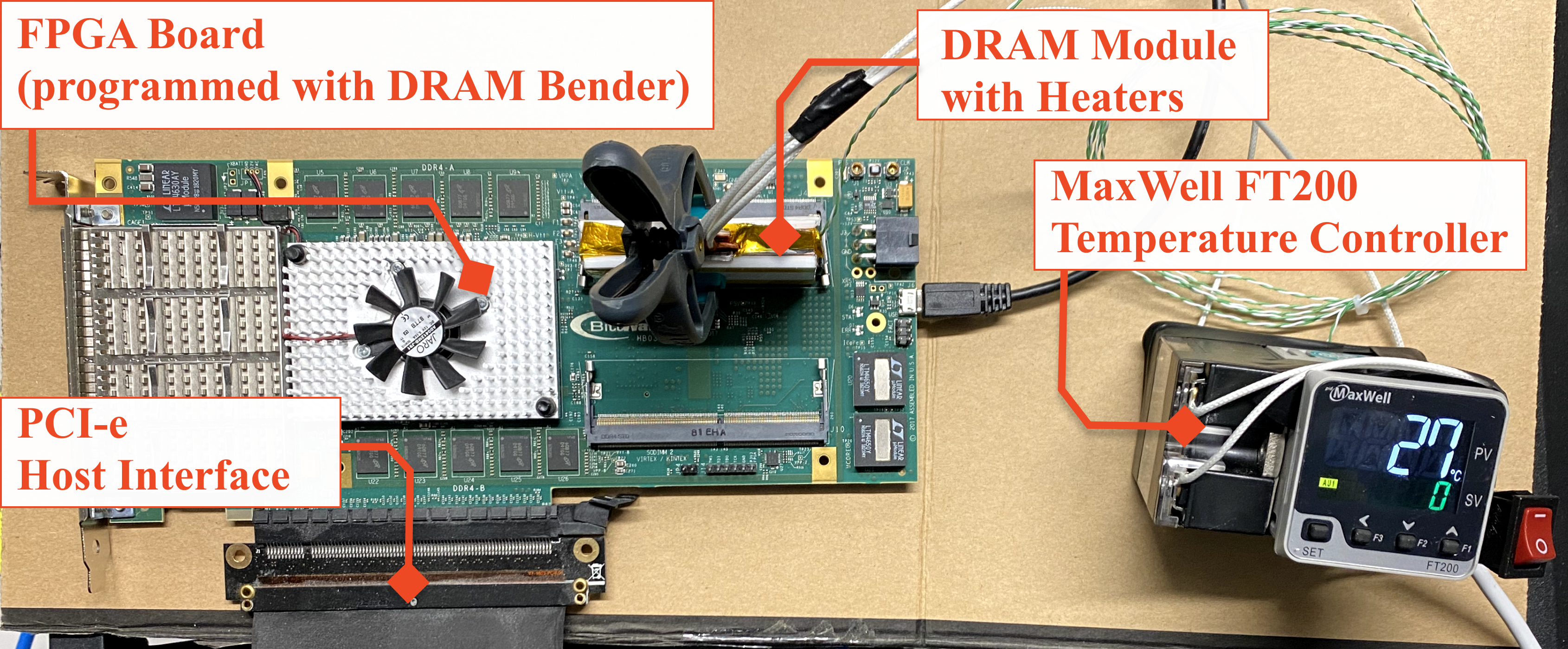
Fig. 2 shows our FPGA-based DRAM testing infrastructure for testing real DDR4 DRAM chips. Our infrastructure consists of four main components: 1) an FPGA development board (Xilinx Alveo U200 [216] for DIMMs or Bittware XUSP3S [217] for SODIMMs), programmed with DRAM Bender [218, 219] to execute our test programs, 2) a host machine that generates the test program and collects experimental results, 3) a thermocouple temperature sensor and a pair of heater pads pressed against the DRAM chips that heat up the DRAM chips to a desired temperature, and 4) a PID temperature controller (MaxWell FT200 [220]) that controls the heaters and keeps the temperature at the desired level with a precision of .444To evaluate temperature stability during RowHammer tests, we perform a double-sided RowHammer test with a hammer count of 1M and traverse across all rows in round-robin fashion for 24 hours at three different temperature levels. We sample the temperature of three modules (one from each manufacturer) every 5 seconds and observe a variation within the error margin of , , and at , , and , respectively.
Eliminating Interference Sources. To observe read disturbance induced bitflips in circuit level, we eliminate perform the best effort to eliminate potential sources of interference to our best ability and control, by taking four measures, similar to the methodology used by prior works [61, 62, 63, 42, 70]. First, we disable periodic refresh during the execution of our test programs to prevent potential on-DRAM-die TRR mechanisms [36, 42] from refreshing victim rows so that we can observe the DRAM chip’s behavior at the circuit-level. Second, we strictly bound the execution time of our test programs within the refresh window of the tested DRAM chips at the tested temperature to avoid data retention failures interfering with read disturbance failures. Third, we run each test ten times and record the smallest (largest) observed () for each row across iterations to account for the worst-case.555We observe a 5.7% variation in the bit error rate across ten iterations. Fourth, we verify that the tested DRAM modules and chips have neither rank-level nor on-die ECC [136, 221]. With these measures, we directly observe and analyze all bitflips without interference.
4.2 Tested DDR4 DRAM Chips
Table 1 shows the 144 real DDR4 DRAM chips (in 15 modules) spanning 10 different chip designs that we test from all three major DRAM manufacturers. To investigate whether our spatial variation analysis applies to different DRAM technologies, designs, and manufacturing processes, we test various DRAM chips with different densities, die revisions, and chip organizations from each DRAM chip manufacturer.666A DRAM chip’s technology node is not always publicly available. We assume that two DRAM chips from the same manufacturer have the same technology node only if they share both 1) the same die density and 2) the same die revision code.
| DIMM | # of | Density | Chip | Date | |
| Mfr. | ID | Chips | Die Rev. | Org. | (ww-yy) |
| Mfr. H (SK Hynix) | H0 | 16Gb – A | x8 | 51-20 | |
| H1, H2, H3 | 16Gb – C | x8 | 48-20 | ||
| H4 | 8Gb – D | x8 | 48-20 | ||
| M0 | 16Gb – E | x16 | 46-20 | ||
| Mfr. M | M1, M3 | 8Gb – B | x4 | N/A | |
| (Micron) | M2 | 16Gb – E | x4 | 14-20 | |
| M4 | 16Gb – B | x16 | 26-21 | ||
| S0, S1 | 8Gb – B | x8 | 52-20 | ||
| Mfr. S | S2 | 8Gb – B | x8 | 10-21 | |
| (Samsung) | S3 | 4Gb – F | x8 | N/A | |
| S4 | 8Gb – C | x4 | 35-21 |
4.3 DRAM Testing Methodology
Metrics. To characterize a DRAM module’s vulnerability to read disturbance, we examine the change in two metrics: 1) the minimum hammer count required to induce the first bitflip (), where we count each pair of activations to the two neighboring rows as one hammer (e.g., one activation each to rows N – 1 and N +1 counts as one hammer) [61], and 2) bit error rate (). A higher () indicates lower (higher) vulnerability to read disturbance.
Tests. Alg. 1 describes our core test loop and two key functions we use: and . All our tests use the double-sided hammering pattern as specified in function and performed similarly by prior works [1, 61, 12, 62, 70]. hammers two physically adjacent (i.e., aggressor) rows to a victim row () in an alternating manner. In this context, one hammer is a pair of activations to the two aggressor rows. The parameter in Alg. 1 defines the hammer count, i.e., the number of activations per aggressor row. The parameter in Alg. 1 defines the time an activated aggressor row remains open. We perform the double-sided hammering in two different ways: 1) with the maximum activation rate possible within DDR4 command timing specifications [148, 149] as this access pattern is stated as the most effective RowHammer access pattern on DRAM chips when RowHammer solutions are disabled [1, 61, 36, 37, 12, 62, 97]; and 2) with keeping aggressor rows open for longer than the minimum charge restoration time ( > ) at each activation to observe the effect of RowPress, a recently demonstrated read disturbance phenomenon, which is different from RowHammer [70]. As function (Alg. 1) demonstrates, we initialize 1) two aggressor rows and one victim row with opposite data patterns to exacerbate read disturbance [61, 35, 31, 32], 2) perform double-sided hammer test, and 3) read-back the data from the victim row and compare against the victim row’s initial data pattern to calculate the bit error rate (BER). Our core test loop sweeps different values, banks, and victim row addresses. First, We test three different values: 1) as the minimum value, 2) as a large enough time window in which a streaming access pattern can fetch the whole content in the activated aggressor row, and 3) as a more realistic time window at which a DRAM row can remain open due to high row buffer hit rate [226, 70]. Second, we sweep through banks 1, 4, 10, and 15 as representative banks from each bank group [148, 98, 219]. Third, we test all rows in a tested bank using 14 different hammer counts and six different data patterns.
Hammer Counts. We conduct our tests by using a set of hammer counts on all DRAM rows instead of finding precisely for each row. This is because significantly varies across rows, and thus, causes a large experiment time (e.g., several weeks or even months) to find at high precision (e.g., within hammers) for each row individually. Therefore, we test the DRAM chips under 14 different hammer counts from to as specified in Alg. 1.777 is (not ) unless otherwise specified.
Data Patterns. We use six commonly used data patterns [118, 120, 130, 128, 129, 61, 119, 227, 62, 1, 109]: row stripe, checkerboard, column stripe, and the opposites of these three data patterns that are shown in Table 2 in detail. We identify the worst-case data pattern () for each row as the data pattern that results in the largest at the hammer count of .888We find that a hammer count of 128K is both 1) low enough to be used in a system-level attack in a real system [36], and 2) high enough to provide a large number of bitflips in all DRAM modules we tested. Then, we sweep the hammer count from 1K to 96K and measure for the WCDP of each row.
| Data Pattern | Aggressor Rows | Victim Row |
| Row Stripe (RS) | ||
| Row Stripe Inverse (RSI) | ||
| Column Stripe (CS) | ||
| Column Stripe Inverse (CSI) | ||
| Checkerboard (CB) | ||
| Checkerboard Inverse (CBI) |
Finding Physically Adjacent Rows. DRAM-internal address mapping schemes [37, 116] are used by DRAM manufacturers to translate logical DRAM addresses (e.g., row, bank, and column) that are exposed over the DRAM interface (to the memory controller) to physical DRAM addresses (e.g., physical location of a row). Internal address mapping schemes allow 1) post-manufacturing row repair techniques to repair erroneous DRAM rows by remapping such rows to spare rows and 2) DRAM manufacturers organize DRAM internals in a cost-optimized way, e.g., by organizing internal DRAM buffers hierarchically [128, 228]. The mapping scheme can substantially vary across different DRAM chips [7, 37, 223, 224, 110, 128, 225, 1, 119, 109, 136, 62, 198, 215]. For every victim DRAM row that we test, we identify the two neighboring physically-adjacent DRAM row addresses that the memory controller can use to access the aggressor rows in a double-sided RowHammer attack. To do so, we reverse-engineer the physical row organization using techniques described in prior works [61, 62].
Temperature. We maintain the DRAM chip temperature at , which is very close to the maximum point of the normal operating condition of [148]. We choose this temperature because prior works show that increasing temperature tends to reduce DRAM chips’ overall realiability [109, 62, 46, 70].999Prior works [62, 70] demonstrate a complex interaction between temperature and a row’s read disturbance (especially RowHammer) vulnerability and suggest that each DRAM chip should be tested at all temperature levels to account for the effect of temperature. Thus, fully understanding the effects of temperature and aging requires extensive characterization studies, requiring many months-long testing time. Therefore, we leave such studies for future work. Due to time and space limitations, we leave a rigorous characterization of temperature’s effect for future work, while presenting the preliminary analysis where we repeat double-sided RowHammer tests at on 5K randomly selected DRAM rows at nine different hammer counts. We observe that the variation in overall with the effect of temperature is less than 0.5%.
5 Spatial Variation in DRAM Read Disturbance
This section presents the first rigorous spatial variation analysis of read disturbance across DRAM rows. Many prior works [1, 61, 88, 55, 54] analyze RowHammer vulnerability at the DRAM bank granularity across many DRAM modules without providing analysis of the variation of this vulnerability across rows. Recent works [62, 63, 70, 97] analyze the variation in RowHammer vulnerability across DRAM rows. However, these analyses are limited to a small subset of DRAM rows (4K to 9K), while a DRAM bank typically has DRAM rows [148, 229, 230, 231, 232, 233, 234, 235, 236, 237]. Thus, prior works might not fully reflect the vulnerability profile of real DRAM chips. Fully characterizing and understanding the vulnerability profile is crucial to avoiding read disturbance bitflips as existing read disturbance solutions must be properly configured based on proper characterization [1, 163, 85, 86, 103, 102, 104, 180, 181]. This section presents a more rigorous and targeted read disturbance characterization study of 144 real DDR4 DRAM chips spanning 10 different chip designs, following the methodology described in §4.
5.1 Bit Error Rate Across DRAM Rows
We investigate the variation in the number of bitflips caused by read disturbance for a hammer count of 128K and of . Fig. 3 shows the distribution of observed for each DRAM row across all tested DRAM banks and modules from three main manufacturers in a box-and-whiskers plot.101010The box is lower-bounded by the first quartile (i.e., the median of the first half of the ordered set of data points) and upper-bounded by the third quartile (i.e., the median of the second half of the ordered set of data points). The interquartile range () is the distance between the first and third quartiles (i.e., box size). Whiskers mark the central 1.5 range, and white circles show the mean values. Each of the three rows of subplots is dedicated to modules from a different manufacturer, and each subplot shows data from a different DRAM module. The x-axis shows the bank address and the y-axis shows the bit error rate (). We annotate each module’s name and variation across rows and banks in terms of the coefficient of variation (CV)111111Coefficient of variation is the standard deviation of a distribution, normalized to the mean [238, 239]. at the bottom of each subplot. We make Obsvs. 5.1-5.1 from Fig. 3.
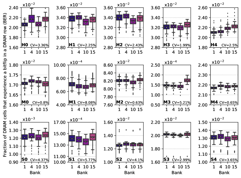
Observation 1. varies across DRAM rows in a DRAM module. For example, DRAM rows in modules M1 and S1 exhibit coefficient of variations (CV) of 8.08% and 5.77%, respectively, on average across all tested banks.
Observation 2. Different banks within the same DRAM module exhibit similar to each other. As the box plots for different banks largely overlap with each other in the y-axis, we observe a smaller variation in across banks compared to across rows in a bank for all tested modules except H4 and M3. For example, the average (minimum/maximum) across all DRAM rows in four different banks of M0 are 1.71% (1.65%/1.73%), 1.71% (1.66%/1.74%), 1.70% (1.64%/1.74%), and 1.72% (1.66%/1.74%).
Observation 3. can significantly vary across different DRAM modules from the same manufacturer. For example, modules M0, M1, and M3 show distributions that are strictly distinct from each other across their mean values. From Obsvs. 5.1-5.1, we draw Takeaway 5.1.
To understand the spatial variation of rows with high and low s, we analyze their locations within their banks. Fig. 4 shows how varies as the row address increases. The x-axis shows a DRAM row’s relative location in its bank, where 0.0 and 1.0 are the two edges of a DRAM bank. The y-axis shows the the corresponding DRAM row experiences at a hammer count of 128K, normalized to the minimum observed across all rows in all tested banks in a module. Each subplot is dedicated to a different manufacturer, and each curve represents a different DRAM module. The shades around the curves show the minimum and maximum values for a given row address across different DRAM banks in a module. We make Obsvs. 5.1 and 5.1 from Fig. 4.
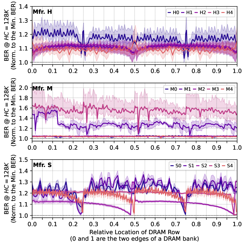
Observation 4. repeatedly increases and decreases with different intervals of row distances in different DRAM modules. For example, curve of S4 follows a repeatedly increasing and decreasing pattern across all rows, where it shows local minimums at 0.25, 0.50, 0.75, and 1.00. We hypothesize that this regularity in variation can be caused by design decisions (design-induced variation), e.g., row’s distance from subarray boundaries and I/O circuitry, as discussed by prior works [119, 62, 97].
Observation 5. Average can vary across large chunks of a DRAM bank. For example, the average (minimum/maximum) normalized in the module M1 across DRAM rows between relative locations 0.03 and 0.12 is 1.51 (1.31 /1.67 ) while it is 1.25 (1.00 /1.42 ) between relative locations 0.20 and 1.00. This discrepancy in across large chunks of rows does not consistently occur across all tested modules. Understanding the root cause of this discrepancy requires extensive knowledge and insights into the circuit design and manufacturing process of the particular DRAM modules exhibiting this behavior. Unfortunately, this piece of information is proprietary and not publicly disclosed by the manufacturers. We hypothesize that the root cause of this discrepancy can be the variation in the manufacturing process, leading to a part of DRAM chip being more vulnerable to read disturbance compared to other parts. From Obsvs. 5.1 and 5.1, we derive Takeaway 5.1.
5.2 Minimum Activation Count to Induce a Bitflip
We investigate the variation in across DRAM rows. To do so, we repeat our tests at 14 different hammer counts from 1K to 128K (Algorithm 1). We define a row’s as the minimum of the tested hammer counts at which the row experiences a bitflip. Fig. 5 shows the distribution of values across rows. Each subplot shows the distribution for a different manufacturer. The x- and y-axes show the values and the fraction of the DRAM rows with the specified value, respectively. Different colors represent different modules. The error bars mark the minimum/maximum of a given value across tested banks. Red vertical dashed line marks the minimum that we observe across all rows in tested modules from a manufacturer. We make Obsvs. 5.2–5.2 from Fig. 5.
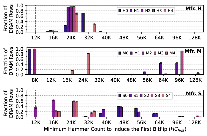
Observation 6. values significantly vary across DRAM rows but not across banks. For example, S0 and S1 contain rows that experience bitflips at hammer counts of 32K and 24K, respectively, while they also have rows that do not experience bitflips until 128K. Despite this large variation, the variation across banks is significantly low, as error bars show.
Observation 7. Different DRAM modules from the same manufacturer can exhibit significantly different distributions. For example, rows from M0 and M4 exhibit values from 8K to 40K and 12K to 96K, respectively.
To understand the spatial variation in across rows, we investigate how a row’s changes with the row’s location within the DRAM bank. Fig. 6 shows the row’s relative location on the x-axis and its , normalized to the minimum observed in the corresponding module. Each subplot corresponds to a different manufacturer, and different modules are color-coded. We make Obsvs. 5.2 and 5.2 from Fig. 6.
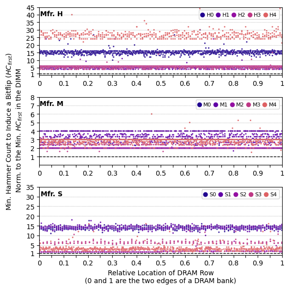
Observation 8. values vary significantly across rows. For example, the module H0 exhibits values that are between and the minimum observed in the bank between relative row addresses 0.02 and 0.03.
Observation 9. Variation in does not exhibit a regular trend as the row address increases. For example, the data points of modules H4 concentrate at the y-axis values of and across all rows in a bank with no regular transition pattern across them. This observation is discrepant with Obsv. 5.1 we have for . The discrepancy across Obsvs. 5.1 and 5.2 shows that although read disturbance vulnerability varies regularly across rows in terms of the fraction of DRAM cells experiencing bitflips, the values across the weakest DRAM cells do not exhibit such a regular variation pattern. From Obsvs. 5.2 and 5.2, we derive Takeaway 5.2.
5.3 Effect of RowPress
We analyze the effect of the recently discovered read disturbance phenomenon, RowPress [70], on the distribution. To do so, we repeat our tests with configurations of and instead of .121212We choose these values because they are large enough to show the effects of RowPress and realistic, such that an adversarial access pattern can easily force these values by accessing different cachelines in a DRAM row. We do not sweep all possible values due to the limitations in experiment time. Fig. 7 shows a box-and-whiskers plot10 of the distribution across all rows in all tested modules under the three different values we test. The x-axis shows the values, and the y-axis shows the values. Different subplots show modules from different manufacturers. We make Obsvs. 5.3 and 5.3 from Fig. 7.
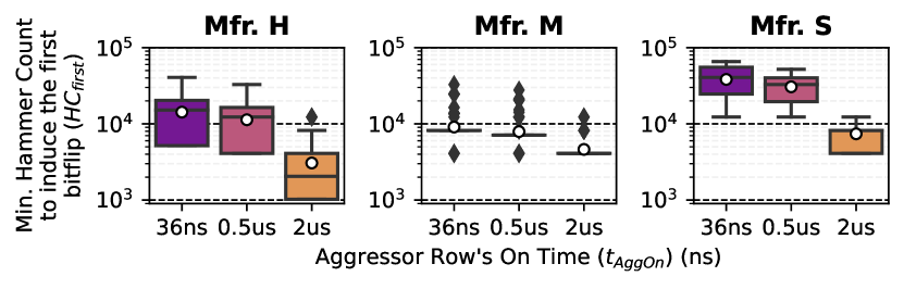
Observation 10. decreases with increasing for the vast majority of DRAM rows. We observe that both mean values and the box () boundaries decrease on the y-axis when increases on the x-axis.
Observation 11. values vary significantly across DRAM rows even when is . For example, distribution across rows in module H2 exhibits the coefficient of variation (CV) values of 25.0%, 23.0%, and 30.4% for values of , , and .
5.4 Spatial Features
This section investigates potential correlations between a DRAM row’s vulnerability to read disturbance and the row’s spatial features. To do so, we consider a set of features that might affect a DRAM row’s reliable operation based on the findings of prior works [240, 241, 118, 119, 133, 62]: 1) bank address, 2) row address, 3) subarray address, 4) row’s distance to the sense amplifiers, i.e., subarray boundaries. To perform this analysis, subarray boundary identification is critical. Unfortunately, this information is not publicly available. To address this problem, we reverse-engineer the subarray boundaries.
5.4.1 Subarray Reverse Engineering
We leverage two key insights.
Key Insight 1. First, a row located at a subarray boundary can be disturbed by hammering or pressing its neighboring rows only on one side of the row instead of both sides. Exploiting this observation, we cluster the DRAM rows based on row address and the number of rows that single-sided hammering or pressing a given row affects. We do so using the k-means clustering algorithm[242]. Because the number of subarrays is initially unknown, we sweep the parameter k and choose the best k value based on the clustering’s silhouette score [243]. As a representative example, Fig. 8 shows the silhouette score of the classification of DRAM rows into subarrays using the k-means algorithm. We sweep the parameter k on the x-axis and show the silhouette score on the y-axis. Different curves represent different modules from Mfr. S.
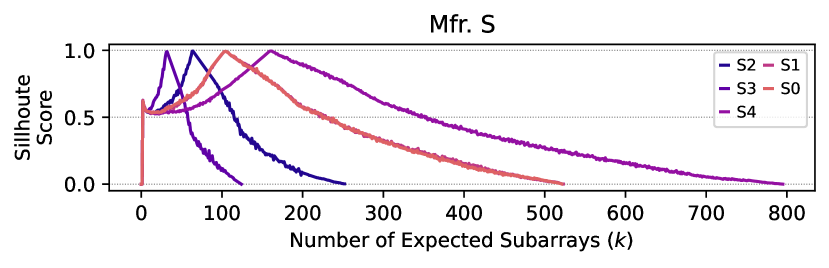
From Fig. 8, we observe that the silhouette score reaches a global maximum and decreases monotonically as we sweep the k-parameter. Based on this observation, we hypothesize that the k-value at the global maximum is the number of subarray boundaries in a DRAM bank, and each cluster for this k-value is a subarray containing the rows in the cluster.
Key Insight 2. Since DRAM rows share a local bitline within a subarray, it is possible to copy one row’s (i.e., source row) data to another row (i.e., destination row) within the same subarray (i.e., also known as the intra-subarray RowClone operation [139]). Prior works [178, 244, 245, 246, 247, 248] already show that it is possible to perform RowClone in off-the-shelf DRAM chips by violating timing constraints such that two rows are activated in quick succession. We conduct RowClone tests following the prior work’s methodology [244]. If the source row’s content is successfully copied to the destination row with no bitflips, both the source and destination rows have to be in the same subarray. However, the opposite case (an unsuccessful RowClone operation) does not necessarily mean that the two rows are in different subarrays. This is because intra-subarray RowClone is not officially supported in existing DRAM chips, and thus not guaranteed to work reliably across all rows in a subarray.
We first identify the candidates of subarray boundaries using Key Insight 1 based on the single-sided RowHammer tests. Second, we test these subarray boundaries using Key Insight 2 based on the intra-subarray RowClone tests such that a successful intra-subarray RowClone operation invalidates a candidate subarray boundary since the source and the destination rows have to be in the same subarray, and thus there cannot be a subarray boundary in between those two rows. Our analysis identifies differently sized subarrays (from 330 to 1027 rows per subarray) and different numbers of subarrays (from 32 to 206 subarrays per bank) across the tested chips. Unfortunately, we do not have the ground truth design to verify our results.
5.4.2 Correlation Analysis
We analyze the correlation between a DRAM row’s spatial features and the row’s value. As spatial features, we take each bit in the binary representation of a DRAM row’s four properties: 1) bank address, 2) row address, 3) subarray address, and 4) row’s distance to the sense amplifiers. We use each of the spatial features for each DRAM row to predict the row’s among 14 tested hammer counts. We compare the prediction and real experiment results to create the confusion matrix [249] and calculate the F1 score [249] for each feature.
Fig. 9 shows the fraction of spatial features that strongly correlate with the row’s . We consider a spatial feature’s correlation with to be stronger if predicting based on the spatial feature results in a larger F1 score. The x-axis sweeps the F1 score threshold from 0 to 1, and the y-axis shows the fraction of spatial features that correlate with with a larger F1 score than the corresponding F1 score threshold. Each subplot shows DRAM modules from a different manufacturer, and each curve represents a different module.
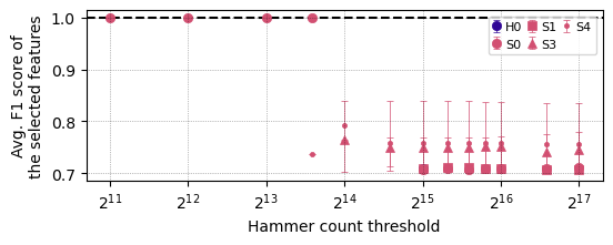
We make three observations from Fig. 9. First, the fraction of spatial features drastically drops when F1 score threshold is increased from 0.6 to 0.7 for all modules. Second, no spatial feature strongly correlates with when F1 score threshold is chosen as 0.8. Third, only four modules (S0, S1, S3, and S4) out of 15 tested modules have spatial features correlating with with an F1 score above 0.7 (not shown in the figure).131313We empirically choose the threshold of 0.7 to filter out spatial features exhibiting a weak correlation with and provide few stronger features. Table 3 shows the set of spatial features that result in an F1 score above 0.7. Ba, Ro, Sa, and Dist. columns show such spatial features from the bank address, row address, subarray address, and the row’s distance to its local sense amplifiers, respectively. The F1 score column shows the average F1 score for the module across all specified features.
| Module | Ba | Ro | Sa | Dist. | F1 Score |
| S0 | Bits 7 and 8 | Bit 0 | Bit 7 | 0.77 | |
| S1 | Bits 7, 8, 10, and 12 | Bit 0 | 0.71 | ||
| S3 | Bit 10 | Bits 1 and 2 | 0.75 | ||
| S4 | Bit 0 | 0.76 |
We make two observations from Table 3. First, the average F1 score among these features does not exceed 0.77 for any tested module. Second, such spatial features mostly come from row and subarray address bits, while no bank bit results in an F1 score larger than 0.7. From these two observations, we draw Takeaway 5.4.2.
5.5 Repeatability and The Effect of Aging
A DRAM row’s read disturbance vulnerability can change over time. A rigorous aging study requires extensively characterizing many DRAM chips many times over a large timespan. Due to time and space limitations, we leave such studies for future work while presenting a preliminary analysis on module H3 as our best effort. We repeat our experiments on one of the tested modules after 68 days of keeping the module under double-sided RowHammer tests at . Fig. 10 demonstrates the effect of aging on in a scatter plot. The x-axis and the y-axis show values before and after aging, respectively. The size of each marker and annotated text near each data point represent the population of DRAM rows at the given before- and after-aging values, normalized to the total population of rows at the before aging, i.e., the population at each x-tick sums up to 1.0. The straight black line marks points, where does not change after aging. We make Obsvs. 5.5 and 5.5 from Fig. 10.
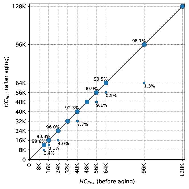
Observation 12. A non-zero fraction of DRAM rows exhibit lower values after aging. For example, 0.4% of DRAM rows with an of 12K before aging experience bitflips at a hammer count of 8K after aging. Therefore, configuring a read disturbance solution for a threshold of 12K is not safe for those 0.4% of the rows, and thus, the values need to be updated online in the field. We believe this result makes a strong case for periodic online testing of DRAM chips, as also proposed by prior works [119, 128, 225, 109, 130, 107, 121, 221].
Observation 13. Rows with the smallest values (weakest rows) get affected by aging, unlike the rows with highest values (strongest rows). For example, values vary with aging on the left-hand-side of the figure while the rows that show an value of 128K exhibit no change in their value. This indicates that the worst-case (the lowest across all rows) changes with aging, and thus aging can jeopardize the security guarantees of existing solutions that are configured based on static identification of the worst-case . Therefore, finding the correct under the effect of aging is a challenge for existing solutions and we call for further research on this topic. Based on Obsvs. 5.5 and 5.5, we draw Takeaway 5.5.
6 Svärd: Spatial Variation Aware Read Disturbance Defenses
We propose a new mechanism Svärd. The goal of Svärd is to reduce the performance overheads induced by existing read disturbance solutions. Svärd achieves this goal by leveraging the variation in read disturbance vulnerability across DRAM rows (§5) to dynamically tune the aggressiveness of existing read disturbance solutions.
6.1 High-Level Overview
Fig. 11 shows Svärd’s high-level overview for its memory controller (MC)-based implementation. Svärd can similarly be implemented within the DRAM chip (§6.2).
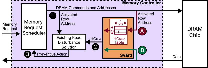
When a DRAM row is activated , both an existing read disturbance solution and Svärd are provided with the activated row address. The existing solution computes a value (e.g., a random number [1] or estimated activation count [103, 85, 102]) to compare against a threshold to decide whether to take a preventive action. Meanwhile , Svärd provides the read disturbance solution with an value based on the activated row’s vulnerability level. Then , the read disturbance solution uses this value to decide whether or not to perform a preventive action. By providing the value based on the row’s characteristics, Svärd tunes the existing solution’s aggressiveness dynamically. Therefore, the read disturbance solution acts either more or less aggressively when a row with high or low vulnerability is accessed. The read disturbance solution does not perform a preventive action (e.g., refresh victim rows, throttle accesses to the aggressor row, or relocate the aggressor row’s content to a far place from the victim row) if the accessed rows do not need the preventive action to avoid bitflips. Svärd maintains a few bits (e.g., 4 bits) to specify the classification of each DRAM row. To do so, Svärd can store and obtain the necessary classification metadata in various ways, including but not limited to: implementing an table within the memory controller that stores as many entries as the number of rows () and fetching the classification data along with the first read from the metadata bits stored in DRAM. Svärd’s classification metadata storage can be optimized by using Bloom filters, similar to prior work [108, 250].
6.2 Implementation Options
Svärd can be implemented where the existing read disturbance solution is implemented. We explain two implementations of Svärd that support read disturbance solutions implemented in 1) the memory controller and 2) in DRAM chips. However, there is a large design space for Svärd’s implementation options that we foreshadow and leave for future research.
Memory Controller. Many prior works [168, 152, 151, 183, 1, 163, 154, 153, 187, 167, 155, 164, 165, 166, 169, 159, 57, 90, 157, 170, 156, 86, 85, 36, 161, 42, 103, 104, 22, 184, 29, 158, 92, 162, 189, 176, 177, 190, 178, 102, 211, 191, 192, 182, 194, 195, 172, 173, 196, 197, 198, 179, 199, 200, 69, 203, 204, 186, 205, 185, 206, 207, 208, 84, 209, 212, 213, 214] propose implementing read disturbance solutions in the memory controller where they can observe and enhance all memory requests. To support these solutions, Svärd maintains a data structure that stores the read disturbance profile of DRAM rows in the memory controller. Svärd observes the row activation () commands that the memory request scheduler issues and uses the activated row address to query the read disturbance profile. In parallel, the read disturbance solution also executes its algorithm (e.g., generates a random number or increments the corresponding activation counters). Svärd provides the read disturbance solution with a more precise threshold corresponding to the activated row’s vulnerability level. The read disturbance solution uses this more precise threshold to decide whether or not to perform a preventive action. Svärd’s implementation can follow one of many common practices of storing metadata in computing systems. Svärd can store its metadata within 1) a hardware data structure (e.g., a table or Bloom filters) in the memory controller, 2) the integrity check bits in the DRAM array [143, 135, 136, 221, 215, 251, 197], or 3) a dedicated memory space in the DRAM array with an optional caching mechanism in the memory controller, similar to prior works [103, 252, 253].
DRAM Chip. Various prior works propose to mitigate read disturbance within the DRAM chip [148, 188, 160, 89, 171, 175, 123, 201, 202, 210]. These read disturbance solutions observe memory access patterns and perform preventive actions within the DRAM chip, transparently to the rest of the system. To support these read disturbance solutions, Svärd can be implemented within the DRAM chip. Similar to the memory controller-based implementation, when a DRAM row is activated, Svärd provides the read disturbance solution with a more precise threshold corresponding to the activated row’s vulnerability level. Svärd can store the necessary metadata within the DRAM array or the activation counters and access when the row is accessed.
6.3 Security
Svärd does not affect the security guarantees of existing read disturbance solutions. Existing read disturbance solutions provide their security guarantees for each DRAM row, conservatively assuming that all DRAM rows are as vulnerable to read disturbance as the most vulnerable (weakest) row. As a result, they overprotect the rows that are stronger than the weakest row. With Svärd, these solutions still provide the same security guarantees for the weakest DRAM rows while at the same time avoiding the overprotection of the rows that are stronger than the weakest rows without compromising their security guarantees. This is because Svärd tunes the aggressiveness of existing solutions based on the vulnerability level of each row.
6.4 Hardware Complexity of Storing the Read Disturbance Vulnerability Profile
The hardware complexity of storing the read disturbance vulnerability profile depends on the size of the profile’s metadata. The size of this metadata can be reduced by grouping DRAM rows using their spatial features if there is a strong correlation between the spatial features of a DRAM row and the row’s . §5.4.2 shows that such correlation exists only for a subset of the tested modules. To make Svärd widely applicable to all DRAM modules, including the ones that do not exhibit such a strong correlation, we evaluate the hardware complexity of storing the read disturbance vulnerability profile for the worst-case, where we cluster rows into several vulnerability bins, and store a bin id separately for each DRAM row. We evaluate two different implementations of this metadata storage: 1) a table in the memory controller and 2) dedicated bits within the data integrity metadata [143, 135, 136, 221, 215, 251, 197] in DRAM. In both cases, we store a vulnerability bin identifier per DRAM row. Because the number of bins in each distribution is smaller than 16, we represent each bin with a 4-bit identifier. For the area overhead analysis, we assume a DRAM bank size of 64K DRAM rows and a DRAM row size of 8KB.
First, for the table implementation, we use CACTI [254] and estimate an area cost of per DRAM bank. When configured for a dual rank system with 16 banks at each rank, the table implementation consumes an overall area overhead of of the chip area of a high-end Intel Xeon processor with four memory channels [255]. This table has an access latency of , which can be completely overlapped with the latency of a row activation, e.g., [256].
Second, storing this metadata as part of the data integrity bits within DRAM requires dedicating four additional bits for an 8KB-large DRAM row. Therefore, it increases the DRAM array size by with a conservative estimate where each row’s width is extended to store four more bits. In this implementation, because the metadata is implemented as part of the data integrity bits, Svärd reads a data word and the metadata in parallel. Therefore, it does not increase the memory access latency. Since the metadata is stored in the DRAM array, the existing read disturbance solution needs to prevent read disturbance bitflips in the metadata. To do so, the read disturbance solution performs its preventive actions (e.g., refreshing a potential victim row) also on the DRAM cells that store the metadata.
7 Performance Evaluation
7.1 Methodology
Simulation Environment. To evaluate the performance impact of Svärd, we conduct cycle-level simulations using Ramulator [257, 258, 259, 260]. Table 4 shows the simulated system configuration.
| Processor |
|
|||||
| DRAM |
|
|||||
|
|
|||||
| Last-Level Cache |
|
In our evaluations, we assume a realistic system with eight cores connected to a memory rank with four bank groups, each containing four banks (16 banks in total). The memory controller employs the FR-FCFS [264, 262] scheduling algorithm with the open-row policy.
Comparison Points. Our baseline does not implement any read disturbance solution and performs memory requests in accordance with DDR4 specifications [148]. We evaluate Svärd with one of five state-of-the-art solutions: AQUA [102], BlockHammer [85], Hydra [103], PARA [1], and RRS [104].12
Workloads. We execute 120 8-core multiprogrammed workload mixes, randomly chosen from five benchmark suites: SPEC CPU2006 [265], SPEC CPU2017 [266], TPC [267], MediaBench [268], and YCSB [269]. We simulate these workloads until each core executes 200M instructions with a warmup period of 100M, similar to prior work [61, 85, 178].
Metrics. We evaluate Svärd’s impact on system throughput (in terms of weighted speedup [270, 271, 272]), job turnaround time (in terms of harmonic speedup [273, 271]), and fairness (in terms of maximum slowdown [274, 114, 115, 275, 276, 111, 277, 278, 279, 280, 281, 85]).
Read Disturbance Vulnerability Profile. To evaluate Svärd, we use each manufacturer’s read disturbance vulnerability profile based on our real chip characterization results (§5). Our evaluation spans seven different worst-case values from 4K down to 64 to evaluate system performance for modern and future DRAM chips as technology node scaling over generations exacerbates read disturbance vulnerability. To apply our read disturbance vulnerability profile to future DRAM chips, we scale down all observed values such that the minimum (worst-case) value in the read disturbance vulnerability profile becomes equal to the value used for evaluating the read disturbance solution without Svärd.
7.2 Performance Analysis
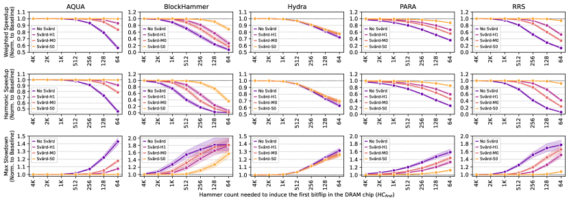
Fig. 12 shows how system performance varies when five state-of-the-art read disturbance solutions are employed with and without Svärd. Each column of subplots evaluates a different read disturbance solution. We sweep on the x-axis from 4K down to 64. We show the three performance metrics (weighted speedup, harmonic speedup, and max. slowdown) normalized to the baseline where no read disturbance solution is implemented. We annotate each configuration of Svärd in the form of Svärd-[DRAM Mfr], where we choose a representative module from each manufacturer. Each marker and shade show the average and the minimum-maximum span of performance measurements across 120 workload mixes. We make Obsvs. 7.2-7.2 from Fig. 12.
Observation 14. Svärd consistently improves system performance in terms of all three metrics when used with any of the five tested solutions for all values below 1K. Svärd configurations result in clearly higher values for weighted and harmonic speedups and lower values for maximum slowdown, compared to the respective solution without Svärd. For an value of 128 (64), Svärd significantly increases system performance over AQUA [102], BlockHammer [85], Hydra [103], PARA [1], and RRS [104] by (), (), (), (), and (), respectively, on average across 120 evaluated workloads and three read disturbance profiles of modules S0, M0, and H1. Svärd’s performance benefits are relatively smaller for Hydra [103] compared to other evaluated read disturbance solutions.This is because Hydra’s performance overheads are not dominated by the preventive refresh operations but the off-chip counter transfer between Hydra’s two key components: the counter cache table within the memory controller and the per-row counter table within the DRAM chip. Svärd reduces Hydra’s preventive refresh operations, but not the off-chip counter transfers. We leave for future work the Hydra-specific optimizations that Svärd might enable.
Observation 15. Svärd performs the best for the distribution profile of S0 among the three evaluated modules. For an of 64, Svärd reduces AQUA’s [102], BlockHammer’s [85], Hydra’s [103], PARA’s [1], and RRS’s [104] performance overheads of 43.51%, 92.29%, 27.75%, 64.08%, 87.40%, down to 0.32% / 16.36% / 6.81%, 31.15% / 82.68% / 73.32%, 22.44% / 23.66% / 22.84%, 12.05% / 44.48% / 33.02%, 5.83% / 65.44% / 47.17%, for modules S0 / M0 / H1, respectively. From Obsvs. 7.2 and 7.2, we draw Takeaway 7.2.
Adversarial Access Patterns. We investigate Svärd’s performance benefits under two adversarial access patterns that exacerbate the performance overheads of Hydra [103] and RRS [104]. Hydra’s adversarial access pattern maximizes the evictions in the counter cache and causes an additional DRAM row activation for each row activation in the steady state. RRS’s adversarial access pattern keeps hammering a DRAM row to maximize the number of row swap operations. Fig. 13 shows the slowdown caused by Hydra (Fig. 13a) and RRS (Fig. 13b) when these read disturbance solutions are used with different Svärd configurations for an of 64. The x-axis shows Svärd’s configurations, and the y-axis shows the measured slowdown (higher is worse), normalized to the slowdown of the evaluated read disturbance solution without Svärd (i.e., No Svärd). We make Obsvs. 7.2 and 7.2 from Fig. 13.
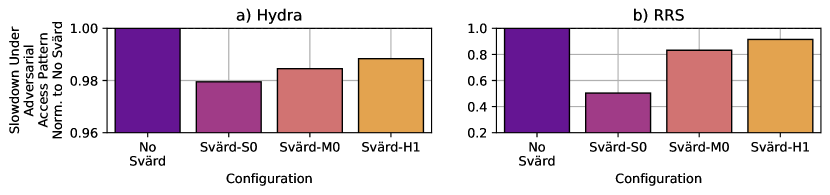
Observation 16. Svärd reduces both Hydra’s and RRS’s performance overheads under adversarial access patterns as all bars except No Svärd are below 1.0 for both Hydra and RRS. For example, Hydra’s and RRS’s performance overheads with no Svärd are 73.1% and 95.6%, respectively (not shown in the Figure), while Svärd reduces these overheads down to 71.6% and 48.2%, respectively, with Mfr. S’s profile.
Observation 17. Similar to Obsv. 7.2, Svärd provides the best performance overhead reduction with module S0’s profile among the three tested profiles. The bars for Svärd-S0 exhibit the lowest slowdown in both Fig. 13a and b.
8 Related Work
This is the first work that 1) rigorously and experimentally analyzes the spatial variation of read disturbance in real DRAM chips and 2) provide a new mechanism that can dynamically adapt the aggressiveness of existing read disturbance mitigation solutions based on the variation profile of real DRAM chips. We highlight our key contributions by contrasting our characterization analysis and proposed mechanism to previous DRAM read disturbance characterization studies and solutions.
Characterization Studies. Six major works extensively characterize the read disturbance in real DRAM chips [1, 61, 62, 63, 97, 70].141414Other prior works [88, 55, 54] present preliminary experimental data from a small number of (three to five) DDR3 DRAM chips. These works use a small sample set of DRAM cells, rows, and chips. First, Kim et al. [1] 1) investigate the vulnerability of 129 commodity DDR3 DRAM modules to various RowHammer attack models; 2) demonstrate for the first time that RowHammer is a real problem for commodity DRAM chips; and 3) characterize RowHammer’s sensitivity to refresh rate and activation rate in terms of , , and the physical distance between aggressor and victim rows. Second, Kim et al. [61] conduct comprehensive scaling experiments on a wide range of 1580 DDR3, DDR4, and LPDDR4 commodity DRAM chips from different DRAM generations and technology nodes, demonstrating that RowHammer has become an even more serious problem over DRAM generations and existing solutions would be expensive for future technology nodes. Third, Orosa et al. [62] rigorously characterize various aspects of the RowHammer vulnerability in real DRAM chips, including the effects of temperature, aggressor row active time, and victim DRAM cell’s physical location on the RowHammer vulnerability. Fourth, Yağlıkçı et al. [63] investigate RowHammer’s sensitivity to wordline voltage and the effects of reducing wordline voltage on DRAM reliability across 272 DRAM chips where 4K rows in a bank is tested in each chip. Fifth, Olgun et al. [97, 282] test an HBM2 DRAM chip’s RowHammer vulnerability and data retention characteristics on a subset of DRAM rows in a DRAM bank with a focus on the spatial variation of RowHammer vulnerability across rows and HBM channels and the characteristics of on-die target row refresh mechanisms. Sixth, Luo et al. [70] are the first to experimentally demonstrate and analyze RowPress, another read disturbance phenomenon, in 164 real DDR4 DRAM chips. They show that RowPress is different from RowHammer, since it 1) affects a different set of DRAM cells from RowHammer and 2) behaves differently from RowHammer as temperature and access pattern change. Unfortunately, these works only analyze a subset of the DRAM rows. In contrast, our paper takes a step further and contributes in three aspects. First, we analyze 1) all DRAM rows in a DRAM bank and 2) a DRAM bank from all four DRAM bank groups in a DRAM rank, which demonstrates the variation in read disturbance vulnerability across rows and banks more accurately and comprehensively. Second, we study the correlation between a row’s spatial features and the row’s read disturbance vulnerability, which requires testing all rows in a DRAM bank. Third, we propose a mechanism that leverages our novel experimental observations to reduce the performance overheads of existing read disturbance solutions.
DRAM Read Disturbance Solutions. Many prior works propose hardware-based [168, 152, 151, 183, 1, 163, 154, 153, 187, 167, 155, 164, 165, 166, 169, 159, 57, 90, 157, 170, 156, 86, 85, 36, 161, 42, 103, 104, 22, 184, 29, 158, 92, 162, 189, 176, 177, 190, 178, 102, 211, 191, 192, 182, 194, 195, 172, 173, 196, 197, 198, 179, 199, 200, 69, 203, 204, 186, 205, 185, 206, 207, 208, 84, 209, 212, 83, 213, 214, 89, 180, 210, 160, 188, 283, 174, 123, 171, 284, 285, 181, 175] and software-based [211, 184, 29, 22, 286, 167, 176] techniques to prevent RowHammer bitflips, including various approaches, e.g., 1) refreshing potential victim rows [151, 152, 153, 154, 155, 156, 157, 158, 159, 160, 161, 86, 162, 163, 164, 165, 166, 167, 168, 1, 169, 170, 171, 36, 42, 172, 103, 173, 174, 175, 176, 177, 178, 179, 180, 181, 182]; 2) selectively throttling memory accesses that might cause bitflips [183, 85]; 3) physically isolating an aggressor row from sensitive data [104, 185, 172, 214, 186, 286, 184, 29, 22, 102, 284, 123]; and 4) enhancing DRAM circuitry to mitigate RowHammer effects [205, 206, 92, 89, 123, 188, 196, 57, 90, 285, 189, 194, 283]. Each approach has different trade-offs in terms of performance impact, energy overhead, hardware complexity, and security guarantees. Our goal in this paper is not to propose a new read disturbance solution, but rather to provide a new method to make the existing solutions more efficient. As we show in §6, on five evaluated state-of-the-art solutions, Svärd can significantly reduce the overheads of read disturbance solutions.
RowHammer Attacks. Many previously proposed RowHammer attacks [3, 4, 5, 6, 7, 8, 9, 10, 1, 11, 12, 13, 14, 15, 16, 17, 18, 19, 20, 21, 22, 23, 24, 25, 26, 27, 28, 29, 30, 31, 32, 33, 34, 35, 36, 37, 38, 39, 40, 41, 42, 43, 44, 45, 46, 47, 48, 49, 50, 51, 52, 53, 71, 72, 73, 74, 75, 76, 77, 78, 79, 80, 81, 82, 83, 84] identify the rows at the desired vulnerability level (e.g., templating) to increase the attack’s success probability. This step fundamentally differs from our characterization because it is enough for an attacker to identify a few rows at the desired vulnerability level. In contrast, as a defense-oriented work, we identify the vulnerability level of all DRAM rows in a DRAM bank to configure read disturbance solutions correctly without compromising their security guarantees. Therefore, this paper presents a significantly more detailed chip-level characterization compared to related attack works.
9 Conclusion
This paper tackles the shortcomings of existing RowHammer solutions by leveraging the spatial variation of read disturbance vulnerability across different memory locations within a memory module. To do so, we 1) present the first rigorous real DRAM chip characterization study of the spatial variation of read disturbance and 2) propose Svärd, a new mechanism that dynamically adapts the aggressiveness of existing solutions to the read disturbance vulnerability of potential victim rows. Our experimental characterization on 144 real DDR4 DRAM chips, spanning 10 different chip designs, demonstrates a large variation in read disturbance vulnerability across different memory locations within a module. By learning and leveraging this large spatial variation in read disturbance vulnerability across DRAM rows, Svärd reduces the performance overheads of state-of-the-art DRAM read disturbance solutions, leading to large system performance benefits. We hope and expect that the understanding we develop via our rigorous experimental characterization and the resulting Svärd technique will inspire DRAM manufacturers and system designers to efficiently and scalably enable robust (i.e., reliable, secure, and safe) operation as DRAM technology node scaling exacerbates read disturbance.
Acknowledgements
We thank the anonymous reviewers of HPCA 2024 for valuable feedback and the SAFARI Research Group members for constructive feedback and the stimulating intellectual environment. We acknowledge the generous gift funding provided by our industrial partners (especially Google, Huawei, Intel, Microsoft), which has been instrumental in enabling the decade-long research we have been conducting on read disturbance in DRAM in particular and memory systems in general. This work was in part supported by the Google Security and Privacy Research Award and the Microsoft Swiss Joint Research Center.
References
- [1] Y. Kim, R. Daly, J. Kim, C. Fallin, J. H. Lee, D. Lee, C. Wilkerson, K. Lai, and O. Mutlu, “Flipping Bits in Memory Without Accessing Them: An Experimental Study of DRAM Disturbance Errors,” in ISCA, 2014.
- [2] R. H. Dennard, “Field-Effect Transistor Memory,” 1968, U.S. Patent 3,387,286.
- [3] A. P. Fournaris, L. Pocero Fraile, and O. Koufopavlou, “Exploiting Hardware Vulnerabilities to Attack Embedded System Devices: A Survey of Potent Microarchitectural Attacks,” Electronics, 2017.
- [4] D. Poddebniak, J. Somorovsky, S. Schinzel, M. Lochter, and P. Rösler, “Attacking Deterministic Signature Schemes using Fault Attacks,” in EuroS&P, 2018.
- [5] A. Tatar, R. K. Konoth, E. Athanasopoulos, C. Giuffrida, H. Bos, and K. Razavi, “Throwhammer: Rowhammer Attacks Over the Network and Defenses,” in USENIX ATC, 2018.
- [6] S. Carre, M. Desjardins, A. Facon, and S. Guilley, “OpenSSL Bellcore’s Protection Helps Fault Attack,” in DSD, 2018.
- [7] A. Barenghi, L. Breveglieri, N. Izzo, and G. Pelosi, “Software-only Reverse Engineering of Physical DRAM Mappings for Rowhammer Attacks,” in IVSW, 2018.
- [8] Z. Zhang, Z. Zhan, D. Balasubramanian, X. Koutsoukos, and G. Karsai, “Triggering Rowhammer Hardware Faults on ARM: A Revisit,” in ASHES, 2018.
- [9] S. Bhattacharya and D. Mukhopadhyay, “Advanced Fault Attacks in Software: Exploiting the Rowhammer Bug,” in Fault Tolerant Architectures for Cryptography and Hardware Security, 2018.
- [10] M. Seaborn and T. Dullien, “Exploiting the DRAM Rowhammer Bug to Gain Kernel Privileges,” http://googleprojectzero.blogspot.com.tr/2015/03/exploiting-dram-rowhammer-bug-to-gain.html, 2015.
- [11] SAFARI Research Group, “RowHammer — GitHub Repository,” https://github.com/CMU-SAFARI/rowhammer, 2014.
- [12] M. Seaborn and T. Dullien, “Exploiting the DRAM Rowhammer Bug to Gain Kernel Privileges,” Black Hat, 2015.
- [13] V. van der Veen, Y. Fratantonio, M. Lindorfer, D. Gruss, C. Maurice, G. Vigna, H. Bos, K. Razavi, and C. Giuffrida, “Drammer: Deterministic Rowhammer Attacks on Mobile Platforms,” in CCS, 2016.
- [14] D. Gruss, C. Maurice, and S. Mangard, “Rowhammer.js: A Remote Software-Induced Fault Attack in Javascript,” in DIMVA, 2016.
- [15] K. Razavi, B. Gras, E. Bosman, B. Preneel, C. Giuffrida, and H. Bos, “Flip Feng Shui: Hammering a Needle in the Software Stack,” in USENIX Security, 2016.
- [16] P. Pessl, D. Gruss, C. Maurice, M. Schwarz, and S. Mangard, “DRAMA: Exploiting DRAM Addressing for Cross-CPU Attacks,” in USENIX Security, 2016.
- [17] Y. Xiao, X. Zhang, Y. Zhang, and R. Teodorescu, “One Bit Flips, One Cloud Flops: Cross-VM Row Hammer Attacks and Privilege Escalation,” in USENIX Security, 2016.
- [18] E. Bosman, K. Razavi, H. Bos, and C. Giuffrida, “Dedup Est Machina: Memory Deduplication as An Advanced Exploitation Vector,” in S&P, 2016.
- [19] S. Bhattacharya and D. Mukhopadhyay, “Curious Case of RowHammer: Flipping Secret Exponent Bits using Timing Analysis,” in CHES, 2016.
- [20] W. Burleson, O. Mutlu, and M. Tiwari, “Invited: Who is the Major Threat to Tomorrow’s Security? You, the Hardware Designer,” in DAC, 2016.
- [21] R. Qiao et al., “A New Approach for RowHammer Attacks,” in HOST, 2016.
- [22] F. Brasser, L. Davi, D. Gens, C. Liebchen, and A.-R. Sadeghi, “Can’t Touch This: Software-Only Mitigation Against Rowhammer Attacks Targeting Kernel Memory,” in USENIX Security, 2017.
- [23] Y. Jang, J. Lee, S. Lee, and T. Kim, “SGX-Bomb: Locking Down the Processor via Rowhammer Attack,” in SysTEX, 2017.
- [24] M. T. Aga, Z. B. Aweke, and T. Austin, “When Good Protections Go Bad: Exploiting Anti-DoS Measures to Accelerate Rowhammer Attacks,” in HOST, 2017.
- [25] O. Mutlu, “The RowHammer Problem and Other Issues We May Face as Memory Becomes Denser,” in DATE, 2017.
- [26] A. Tatar, C. Giuffrida, H. Bos, and K. Razavi, “Defeating Software Mitigations Against Rowhammer: A Surgical Precision Hammer,” in RAID, 2018.
- [27] D. Gruss, M. Lipp, M. Schwarz, D. Genkin, J. Juffinger, S. O’Connell, W. Schoechl, and Y. Yarom, “Another Flip in the Wall of Rowhammer Defenses,” in S&P, 2018.
- [28] M. Lipp, M. T. Aga, M. Schwarz, D. Gruss, C. Maurice, L. Raab, and L. Lamster, “Nethammer: Inducing Rowhammer Faults Through Network Requests,” arXiv:1805.04956, 2018.
- [29] V. van der Veen, M. Lindorfer, Y. Fratantonio, H. P. Pillai, G. Vigna, C. Kruegel, H. Bos, and K. Razavi, “GuardION: Practical Mitigation of DMA-Based Rowhammer Attacks on ARM,” in DIMVA, 2018.
- [30] P. Frigo, C. Giuffrida, H. Bos, and K. Razavi, “Grand Pwning Unit: Accelerating Microarchitectural Attacks with the GPU,” in S&P, 2018.
- [31] L. Cojocar, K. Razavi, C. Giuffrida, and H. Bos, “Exploiting Correcting Codes: On the Effectiveness of ECC Memory Against Rowhammer Attacks,” in S&P, 2019.
- [32] S. Ji, Y. Ko, S. Oh, and J. Kim, “Pinpoint Rowhammer: Suppressing Unwanted Bit Flips on Rowhammer Attacks,” in ASIACCS, 2019.
- [33] O. Mutlu, “RowHammer and Beyond,” in COSADE, 2019.
- [34] S. Hong, P. Frigo, Y. Kaya, C. Giuffrida, and T. Dumitras, “Terminal Brain Damage: Exposing the Graceless Degradation in Deep Neural Networks Under Hardware Fault Attacks,” in USENIX Security, 2019.
- [35] A. Kwong, D. Genkin, D. Gruss, and Y. Yarom, “RAMBleed: Reading Bits in Memory Without Accessing Them,” in S&P, 2020.
- [36] P. Frigo, E. Vannacci, H. Hassan, V. van der Veen, O. Mutlu, C. Giuffrida, H. Bos, and K. Razavi, “TRRespass: Exploiting the Many Sides of Target Row Refresh,” in S&P, 2020.
- [37] L. Cojocar, J. Kim, M. Patel, L. Tsai, S. Saroiu, A. Wolman, and O. Mutlu, “Are We Susceptible to Rowhammer? An End-to-End Methodology for Cloud Providers,” in S&P, 2020.
- [38] Z. Weissman, T. Tiemann, D. Moghimi, E. Custodio, T. Eisenbarth, and B. Sunar, “JackHammer: Efficient Rowhammer on Heterogeneous FPGA–CPU Platforms,” arXiv:1912.11523, 2020.
- [39] Z. Zhang, Y. Cheng, D. Liu, S. Nepal, Z. Wang, and Y. Yarom, “PTHammer: Cross-User-Kernel-Boundary Rowhammer Through Implicit Accesses,” in MICRO, 2020.
- [40] F. Yao, A. S. Rakin, and D. Fan, “Deephammer: Depleting the Intelligence of Deep Neural Networks Through Targeted Chain of Bit Flips,” in USENIX Security, 2020.
- [41] F. de Ridder, P. Frigo, E. Vannacci, H. Bos, C. Giuffrida, and K. Razavi, “SMASH: Synchronized Many-Sided Rowhammer Attacks from JavaScript,” in USENIX Security, 2021.
- [42] H. Hassan, Y. C. Tugrul, J. S. Kim, V. van der Veen, K. Razavi, and O. Mutlu, “Uncovering In-DRAM RowHammer Protection Mechanisms: A New Methodology, Custom RowHammer Patterns, and Implications,” in MICRO, 2021.
- [43] P. Jattke, V. van der Veen, P. Frigo, S. Gunter, and K. Razavi, “Blacksmith: Scalable Rowhammering in the Frequency Domain,” in S&P, 2022.
- [44] M. C. Tol, S. Islam, B. Sunar, and Z. Zhang, “Toward Realistic Backdoor Injection Attacks on DNNs using RowHammer,” arXiv:2110.07683, 2022.
- [45] A. Kogler, J. Juffinger, S. Qazi, Y. Kim, M. Lipp, N. Boichat, E. Shiu, M. Nissler, and D. Gruss, “Half-Double: Hammering From the Next Row Over,” in USENIX Security, 2022.
- [46] L. Orosa, U. Rührmair, A. G. Yaglikci, H. Luo, A. Olgun, P. Jattke, M. Patel, J. Kim, K. Razavi, and O. Mutlu, “SpyHammer: Using RowHammer to Remotely Spy on Temperature,” arXiv:2210.04084, 2022.
- [47] Z. Zhang, W. He, Y. Cheng, W. Wang, Y. Gao, D. Liu, K. Li, S. Nepal, A. Fu, and Y. Zou, “Implicit Hammer: Cross-Privilege-Boundary Rowhammer through Implicit Accesses,” IEEE TDSC, 2022.
- [48] L. Liu, Y. Guo, Y. Cheng, Y. Zhang, and J. Yang, “Generating Robust DNN with Resistance to Bit-Flip based Adversarial Weight Attack,” IEEE TC, 2022.
- [49] Y. Cohen, K. S. Tharayil, A. Haenel, D. Genkin, A. D. Keromytis, Y. Oren, and Y. Yarom, “HammerScope: Observing DRAM Power Consumption Using Rowhammer,” in CCS, 2022.
- [50] M. Zheng, Q. Lou, and L. Jiang, “TrojViT: Trojan Insertion in Vision Transformers,” arXiv:2208.13049, 2022.
- [51] M. Fahr Jr, H. Kippen, A. Kwong, T. Dang, J. Lichtinger, D. Dachman-Soled, D. Genkin, A. Nelson, R. Perlner, A. Yerukhimovich et al., “When Frodo Flips: End-to-End Key Recovery on FrodoKEM via Rowhammer,” CCS, 2022.
- [52] Y. Tobah, A. Kwong, I. Kang, D. Genkin, and K. G. Shin, “SpecHammer: Combining Spectre and Rowhammer for New Speculative Attacks,” in S&P, 2022.
- [53] A. S. Rakin, M. H. I. Chowdhuryy, F. Yao, and D. Fan, “DeepSteal: Advanced Model Extractions Leveraging Efficient Weight Stealing in Memories,” in S&P, 2022.
- [54] K. Park, D. Yun, and S. Baeg, “Statistical Distributions of Row-hammering Induced Failures in DDR3 Components,” Microelectronics Reliability, 2016.
- [55] K. Park, C. Lim, D. Yun, and S. Baeg, “Experiments and Root Cause Analysis for Active-precharge Hammering Fault in DDR3 SDRAM under 3 nm Technology,” Microelectronics Reliability, 2016.
- [56] C. Lim, K. Park, and S. Baeg, “Active Precharge Hammering to Monitor Displacement Damage Using High-Energy Protons in 3x-nm SDRAM,” TNS, 2017.
- [57] S.-W. Ryu, K. Min, J. Shin, H. Kwon, D. Nam, T. Oh, T.-S. Jang, M. Yoo, Y. Kim, and S. Hong, “Overcoming the Reliability Limitation in the Ultimately Scaled DRAM using Silicon Migration Technique by Hydrogen Annealing,” in IEDM, 2017.
- [58] D. Yun, M. Park, C. Lim, and S. Baeg, “Study of TID Effects on One Row Hammering using Gamma in DDR4 SDRAMs,” in IRPS, 2018.
- [59] T. Yang and X.-W. Lin, “Trap-Assisted DRAM Row Hammer Effect,” EDL, 2019.
- [60] A. J. Walker, S. Lee, and D. Beery, “On DRAM RowHammer and the Physics on Insecurity,” IEEE TED, 2021.
- [61] J. S. Kim, M. Patel, A. G. Yağlıkcı, H. Hassan, R. Azizi, L. Orosa, and O. Mutlu, “Revisiting RowHammer: An Experimental Analysis of Modern Devices and Mitigation Techniques,” in ISCA, 2020.
- [62] L. Orosa, A. G. Yağlıkcı, H. Luo, A. Olgun, J. Park, H. Hassan, M. Patel, J. S. Kim, and O. Mutlu, “A Deeper Look into RowHammer’s Sensitivities: Experimental Analysis of Real DRAM Chips and Implications on Future Attacks and Defenses,” in MICRO, 2021.
- [63] A. G. Yağlıkcı, H. Luo, G. F. De Oliviera, A. Olgun, M. Patel, J. Park, H. Hassan, J. S. Kim, L. Orosa, and O. Mutlu, “Understanding RowHammer Under Reduced Wordline Voltage: An Experimental Study Using Real DRAM Devices,” in DSN, 2022.
- [64] M. N. I. Khan and S. Ghosh, “Analysis of Row Hammer Attack on STTRAM,” in ICCD, 2018.
- [65] S. Agarwal, H. Dixit, D. Datta, M. Tran, D. Houssameddine, D. Shum, and F. Benistant, “Rowhammer for Spin Torque based Memory: Problem or Not?” in INTERMAG, 2018.
- [66] H. Li, H.-Y. Chen, Z. Chen, B. Chen, R. Liu, G. Qiu, P. Huang, F. Zhang, Z. Jiang, B. Gao, L. Liu, X. Liu, S. Yu, H.-S. P. Wong, and J. Kang, “Write Disturb Analyses on Half-Selected Cells of Cross-Point RRAM Arrays,” in IRPS, 2014.
- [67] K. Ni, X. Li, J. A. Smith, M. Jerry, and S. Datta, “Write Disturb in Ferroelectric FETs and Its Implication for 1T-FeFET AND Memory Arrays,” IEEE EDL, 2018.
- [68] P. R. Genssler, V. M. van Santen, J. Henkel, and H. Amrouch, “On the Reliability of FeFET On-Chip Memory,” TC, 2022.
- [69] O. Mutlu, A. Olgun, and A. G. Yaglikci, “Fundamentally Understanding and Solving RowHammer,” in ASP-DAC, 2023.
- [70] H. Luo, A. Olgun, A. G. Yağlıkcı, Y. C. Tuğrul, S. Rhyner, M. B. Cavlak, J. Lindegger, M. Sadrosadati, and O. Mutlu, “RowPress: Amplifying Read Disturbance in Modern DRAM Chips,” in ISCA, 2023.
- [71] H. Aydin and A. Sertbaş, “Cyber Security in Industrial Control Systems (ICS): A Survey of RowHammer Vulnerability,” Applied Computer Science, 2022.
- [72] K. Mus, Y. Doröz, M. C. Tol, K. Rahman, and B. Sunar, “Jolt: Recovering TLS Signing Keys via Rowhammer Faults,” Cryptology ePrint Archive, 2022.
- [73] J. Wang, H. Xu, C. Xiao, L. Zhang, and Y. Zheng, “Research and Implementation of Rowhammer Attack Method based on Domestic NeoKylin Operating System,” in ICFTIC, 2022.
- [74] S. Lefforge, “Reverse Engineering Post-Quantum Cryptography Schemes to Find Rowhammer Exploits,” Bachelor’s Thesis, University of Arkansas, 2023.
- [75] M. J. Fahr, “The Effects of Side-Channel Attacks on Post-Quantum Cryptography: Influencing FrodoKEM Key Generation Using the Rowhammer Exploit,” Master’s thesis, University of Arkansas, 2022.
- [76] A. Kaur, P. Srivastav, and B. Ghoshal, “Work-in-Progress: DRAM-MaUT: DRAM Address Mapping Unveiling Tool for ARM Devices,” in CASES, 2022.
- [77] K. Cai, Z. Zhang, and F. Yao, “On the Feasibility of Training-time Trojan Attacks through Hardware-based Faults in Memory,” in HOST, 2022.
- [78] D. Li, D. Liu, Y. Ren, Z. Wang, Y. Sun, Z. Guan, Q. Wu, and J. Liu, “CyberRadar: A PUF-based Detecting and Mapping Framework for Physical Devices,” arXiv:2201.07597, 2022.
- [79] A. Roohi and S. Angizi, “Efficient Targeted Bit-Flip Attack Against the Local Binary Pattern Network,” in HOST, 2022.
- [80] F. Staudigl, H. Al Indari, D. Schön, D. Sisejkovic, F. Merchant, J. M. Joseph, V. Rana, S. Menzel, and R. Leupers, “NeuroHammer: Inducing Bit-Flips in Memristive Crossbar Memories,” in DATE, 2022.
- [81] L.-H. Yang, S.-S. Huang, T.-L. Cheng, Y.-C. Kuo, and J.-J. Kuo, “Socially-Aware Collaborative Defense System against Bit-Flip Attack in Social Internet of Things and Its Online Assignment Optimization,” in ICCCN, 2022.
- [82] S. Islam, K. Mus, R. Singh, P. Schaumont, and B. Sunar, “Signature Correction Attack on Dilithium Signature Scheme,” in Euro S&P, 2022.
- [83] C. Tomita, M. Takita, K. Fukushima, Y. Nakano, Y. Shiraishi, and M. Morii, “Extracting the secrets of openssl with rambleed,” Sensors, 2022.
- [84] L. France, F. Bruguier, M. Mushtaq, D. Novo, and P. Benoit, “Modeling Rowhammer in the gem5 Simulator,” in CHES 2022-Conference on Cryptographic Hardware and Embedded Systems, 2022.
- [85] A. G. Yağlıkcı, M. Patel, J. S. Kim, R. Azizibarzoki, A. Olgun, L. Orosa, H. Hassan, J. Park, K. Kanellopoullos, T. Shahroodi, S. Ghose, and O. Mutlu, “BlockHammer: Preventing RowHammer at Low Cost by Blacklisting Rapidly-Accessed DRAM Rows,” in HPCA, 2021.
- [86] Y. Park, W. Kwon, E. Lee, T. J. Ham, J. H. Ahn, and J. W. Lee, “Graphene: Strong yet Lightweight Row Hammer Protection,” in MICRO, 2020.
- [87] M. Redeker, B. F. Cockburn, and D. G. Elliott, “An Investigation into Crosstalk Noise in DRAM Structures,” in MTDT, 2002.
- [88] K. Park, S. Baeg, S. Wen, and R. Wong, “Active-Precharge Hammering on a Row-Induced Failure in DDR3 SDRAMs Under 3x nm Technology,” in IIRW, 2014.
- [89] C. Yang, C. K. Wei, Y. J. Chang, T. C. Wu, H. P. Chen, and C. S. Lai, “Suppression of RowHammer Effect by Doping Profile Modification in Saddle-Fin Array Devices for Sub-30-nm DRAM Technology,” TDMR, 2016.
- [90] C.-M. Yang, C.-K. Wei, H.-P. Chen, J.-S. Luo, Y. J. Chang, T.-C. Wu, and C.-S. Lai, “Scanning Spreading Resistance Microscopy for Doping Profile in Saddle-Fin Devices,” IEEE Transactions on Nanotechnology, 2017.
- [91] C. Lim, K. Park, G. Bak, D. Yun, M. Park, S. Baeg, S.-J. Wen, and R. Wong, “Study of Proton Radiation Effect to Row Hammer Fault in DDR4 SDRAMs,” Microelectronics Reliability, 2018.
- [92] S. Gautam, S. Manhas, A. Kumar, M. Pakala, and E. Yieh, “Row Hammering Mitigation Using Metal Nanowire in Saddle Fin DRAM,” IEEE TED, 2019.
- [93] Y. Jiang, H. Zhu, D. Sullivan, X. Guo, X. Zhang, and Y. Jin, “Quantifying RowHammer Vulnerability for DRAM Security,” in DAC, 2021.
- [94] W. He, Z. Zhang, Y. Cheng, W. Wang, W. Song, Y. Gao, Q. Zhang, K. Li, D. Liu, and S. Nepal, “WhistleBlower: A System-level Empirical Study on RowHammer,” IEEE Transactions on Computers, 2023.
- [95] S. Baeg, D. Yun, M. Chun, and S.-J. Wen, “Estimation of the Trap Energy Characteristics of Row Hammer-Affected Cells in Gamma-Irradiated DDR4 DRAM,” IEEE Transactions on Nuclear Science, 2022.
- [96] O. Mutlu, “RowHammer,” https://people.inf.ethz.ch/omutlu/pub/onur-Rowhammer-TopPicksinHardwareEmbeddedSecurity-November-8-2018.pdf, 2018, Top Picks in Hardware and Embedded Security.
- [97] A. Olgun, M. Osseiran, A. G. Yaglikci, Y. C. Tugrul, H. Luo, S. Rhyner, B. Salami, J. Gomez Luna, and O. Mutlu, “An Experimental Analysis of RowHammer in HBM2 DRAM Chips,” in DSN Disrupt, 2023.
- [98] A. Olgun, H. Hassan, A. G. Yağlıkcı, Y. C. Tuğrul, L. Orosa, H. Luo, M. Patel, E. Oğuz, and O. Mutlu, “DRAM Bender: An Extensible and Versatile FPGA-based Infrastructure to Easily Test State-of-the-art DRAM Chips,” TCAD, 2023.
- [99] L. Zhou, J. Li, Z. Qiao, P. Ren, Z. Sun, J. Wang, B. Wu, Z. Ji, R. Wang, K. Cao, and R. Huang, “Double-sided Row Hammer Effect in Sub-20 nm DRAM: Physical Mechanism, Key Features and Mitigation,” in IRPS, 2023.
- [100] T. Alsop, “DRAM Manufacturers Revenue Share Worldwide from 2011 to 2022, by Quarter,” https://www.statista.com/statistics/271726/global-market-share-held-by-dram-chip-vendors-since-2010, 2023.
- [101] E. Wang, “Due to Falling Shipments and Prices, Global DRAM Revenue for 3Q22 Showed QoQ Drop of Almost 30%—Unprecedented Since 2008 Financial Crisis,” https://www.trendforce.com/presscenter/news/20221116-11459.html, 2022.
- [102] A. Saxena, G. Saileshwar, P. J. Nair, and M. Qureshi, “AQUA: Scalable Rowhammer Mitigation by Quarantining Aggressor Rows at Runtime,” in MICRO, 2022.
- [103] M. Qureshi, A. Rohan, G. Saileshwar, and P. J. Nair, “Hydra: Enabling Low-Overhead Mitigation of Row-Hammer at Ultra-Low Thresholds via Hybrid Tracking,” in ISCA, 2022.
- [104] G. Saileshwar, B. Wang, M. Qureshi, and P. J. Nair, “Randomized Row-Swap: Mitigating Row Hammer by Breaking Spatial Correlation Between Aggressor and Victim Rows,” in ASPLOS, 2022.
- [105] E. Ipek, O. Mutlu, J. F. Martínez, and R. Caruana, “Self-Optimizing Memory Controllers: A Reinforcement Learning Approach,” in ISCA, 2008.
- [106] T. Zhang, K. Chen, C. Xu, G. Sun, T. Wang, and Y. Xie, “Half-DRAM: A High-Bandwidth and Low-Power DRAM Architecture from the Rethinking of Fine-Grained Activation,” in ISCA, 2014.
- [107] M. Qureshi, D.-H. Kim, S. Khan, P. Nair, and O. Mutlu, “AVATAR: A Variable-Retention-Time (VRT) Aware Refresh for DRAM Systems,” in DSN, 2015.
- [108] J. Liu, B. Jaiyen, R. Veras, and O. Mutlu, “RAIDR: Retention-Aware Intelligent DRAM Refresh,” in ISCA, 2012.
- [109] J. Liu, B. Jaiyen, Y. Kim, C. Wilkerson, O. Mutlu, J. Liu, B. Jaiyen, Y. Kim, C. Wilkerson, and O. Mutlu, “An Experimental Study of Data Retention Behavior in Modern DRAM Devices,” in ISCA, 2013.
- [110] B. Keeth and R. Baker, DRAM Circuit Design: A Tutorial. Wiley, 2001.
- [111] O. Mutlu and T. Moscibroda, “Stall-Time Fair Memory Access Scheduling for Chip Multiprocessors,” in MICRO, 2007.
- [112] T. Moscibroda and O. Mutlu, “Memory Performance Attacks: Denial of Memory Service in Multi-Core Systems,” in USENIX Security, 2007.
- [113] O. Mutlu and T. Moscibroda, “Parallelism-Aware Batch Scheduling: Enhancing Both Performance and Fairness of Shared DRAM Systems,” in ISCA, 2008.
- [114] Y. Kim, D. Han, O. Mutlu, and M. Harchol-Balter, “ATLAS: A Scalable and High-Performance Scheduling Algorithm for Multiple Memory Controllers,” in HPCA, 2010.
- [115] L. Subramanian, D. Lee, V. Seshadri, H. Rastogi, and O. Mutlu, “The Blacklisting Memory Scheduler: Achieving High Performance and Fairness at Low Cost,” in ICCD, 2014.
- [116] Y. Kim et al., “A Case for Subarray-Level Parallelism (SALP) in DRAM,” in ISCA, 2012.
- [117] H. Hassan, G. Pekhimenko, N. Vijaykumar, V. Seshadri, D. Lee, O. Ergin, and O. Mutlu, “ChargeCache: Reducing DRAM Latency by Exploiting Row Access Locality,” in HPCA, 2016.
- [118] K. K. Chang, A. Kashyap, H. Hassan, S. Ghose, K. Hsieh, D. Lee, T. Li, G. Pekhimenko, S. Khan, and O. Mutlu, “Understanding Latency Variation in Modern DRAM Chips: Experimental Characterization, Analysis, and Optimization,” in SIGMETRICS, 2016.
- [119] D. Lee, S. Khan, L. Subramanian, S. Ghose, R. Ausavarungnirun, G. Pekhimenko, V. Seshadri, and O. Mutlu, “Design-induced Latency Variation in Modern DRAM Chips: Characterization, Analysis, and Latency Reduction Mechanisms,” POMACS, 2017.
- [120] K. K. Chang, A. G. Yağlıkcı, S. Ghose, A. Agrawal, N. Chatterjee, A. Kashyap, D. Lee, M. O’Connor, H. Hassan, and O. Mutlu, “Understanding Reduced-Voltage Operation in Modern DRAM Devices: Experimental Characterization, Analysis, and Mechanisms,” in SIGMETRICS, 2017.
- [121] M. Patel, J. S. Kim, and O. Mutlu, “The Reach Profiler (REAPER): Enabling the Mitigation of DRAM Retention Failures via Profiling at Aggressive Conditions,” in ISCA, 2017.
- [122] J. S. Kim, M. Patel, H. Hassan, and O. Mutlu, “The DRAM Latency PUF: Quickly Evaluating Physical Unclonable Functions by Exploiting the Latency-Reliability Tradeoff in Modern Commodity DRAM Devices,” in HPCA, 2018.
- [123] H. Hassan, M. Patel, J. S. Kim, A. G. Yağlıkcı, N. Vijaykumar, N. Mansouri Ghiasi, S. Ghose, and O. Mutlu, “CROW: A Low-Cost Substrate for Improving DRAM Performance, Energy Efficiency, and Reliability,” in ISCA, 2019.
- [124] K. K. Chang, D. Lee, Z. Chishti, A. R. Alameldeen, C. Wilkerson, Y. Kim, and O. Mutlu, “Improving DRAM Performance by Parallelizing Refreshes with Accesses,” in HPCA, 2014.
- [125] K. K. Chang, P. J. Nair, D. Lee, S. Ghose, M. K. Qureshi, and O. Mutlu, “Low-Cost Inter-Linked Subarrays (LISA): Enabling Fast Inter-Subarray Data Movement in DRAM,” in HPCA, 2016.
- [126] S. Ghose, A. G. Yağlıkcı, R. Gupta, D. Lee, K. Kudrolli, W. Liu, H. Hassan, K. Chang, N. Chatterjee, A. Agrawal, M. O’Connor, and O. Mutlu, “What Your DRAM Power Models Are Not Telling You: Lessons from a Detailed Experimental Study,” in SIGMETRICS, 2018.
- [127] H. Hassan, N. Vijaykumar, S. Khan, S. Ghose, K. Chang, G. Pekhimenko, D. Lee, O. Ergin, and O. Mutlu, “SoftMC: A Flexible and Practical Open-Source Infrastructure for Enabling Experimental DRAM Studies,” in HPCA, 2017.
- [128] S. Khan, D. Lee, and O. Mutlu, “PARBOR: An Efficient System-Level Technique to Detect Data-Dependent Failures in DRAM,” in DSN, 2016.
- [129] S. Khan, C. Wilkerson, D. Lee, A. R. Alameldeen, and O. Mutlu, “A Case for Memory Content-Based Detection and Mitigation of Data-Dependent Failures in DRAM,” IEEE CAL, 2016.
- [130] S. Khan, D. Lee, Y. Kim, A. R. Alameldeen, C. Wilkerson, and O. Mutlu, “The Efficacy of Error Mitigation Techniques for DRAM Retention Failures: A Comparative Experimental Study,” in SIGMETRICS, 2014.
- [131] V. Seshadri, T. Mullins, A. Boroumand, O. Mutlu, P. B. Gibbons, M. A. Kozuch, and T. C. Mowry, “Gather-Scatter DRAM: In-DRAM Address Translation to Improve the Spatial Locality of Non-Unit Strided Accesses,” in MICRO, 2015.
- [132] V. Seshadri, D. Lee, T. Mullins, H. Hassan, A. Boroumand, J. Kim, M. A. Kozuch, O. Mutlu, P. B. Gibbons, and T. C. Mowry, “Ambit: In-memory Accelerator for Bulk Bitwise Operations using Commodity DRAM Technology,” in MICRO, 2017.
- [133] J. S. Kim, M. Patel, H. Hassan, and O. Mutlu, “Solar-DRAM: Reducing DRAM Access Latency by Exploiting the Variation in Local Bitlines,” in ICCD, 2018.
- [134] J. S. Kim, M. Patel, H. Hassan, L. Orosa, and O. Mutlu, “D-RaNGe: Using Commodity DRAM Devices to Generate True Random Numbers with Low Latency and High Throughput,” in HPCA, 2019.
- [135] M. Patel, J. S. Kim, H. Hassan, and O. Mutlu, “Understanding and Modeling On-Die Error Correction in Modern DRAM: An Experimental Study Using Real Devices,” in DSN, 2019.
- [136] M. Patel, J. Kim, T. Shahroodi, H. Hassan, and O. Mutlu, “Bit-Exact ECC Recovery (BEER): Determining DRAM On-Die ECC Functions by Exploiting DRAM Data Retention Characteristics,” in MICRO, 2020.
- [137] D. Lee, Y. Kim, V. Seshadri, J. Liu, L. Subramanian, and O. Mutlu, “Tiered-Latency DRAM: A Low Latency and Low Cost DRAM Architecture,” in HPCA, 2013.
- [138] D. Lee, L. Subramanian, R. Ausavarungnirun, J. Choi, and O. Mutlu, “Decoupled Direct Memory Access: Isolating CPU and IO Traffic by Leveraging a Dual-Data-Port DRAM,” in PACT, 2015.
- [139] V. Seshadri, Y. Kim, C. Fallin, D. Lee, R. Ausavarungnirun, G. Pekhimenko, Y. Luo, O. Mutlu, P. B. Gibbons, M. A. Kozuch, and T. Mowry, “RowClone: Fast and Energy-Efficient In-DRAM Bulk Data Copy and Initialization,” in MICRO, 2013.
- [140] H. Luo, T. Shahroodi, H. Hassan, M. Patel, A. G. Yağlıkcı, L. Orosa, J. Park, and O. Mutlu, “CLR-DRAM: A Low-Cost DRAM Architecture Enabling Dynamic Capacity-Latency Trade-Off,” in ISCA, 2020.
- [141] V. Seshadri and O. Mutlu, “In-DRAM Bulk Bitwise Execution Engine,” arXiv:1905.09822, 2019.
- [142] Y. Wang, L. Orosa, X. Peng, Y. Guo, S. Ghose, M. Patel, J. S. Kim, J. G. Luna, M. Sadrosadati, N. M. Ghiasi et al., “FIGARO: Improving System Performance via Fine-Grained In-DRAM Data Relocation and Caching,” in MICRO, 2020.
- [143] JEDEC, JESD79-5: DDR5 SDRAM Standard, 2020.
- [144] JEDEC, JESD209-5A: LPDDR5 SDRAM Standard, 2020.
- [145] JEDEC, JESD209-4B: Low Power Double Data Rate 4 (LPDDR4) Standard, 2017.
- [146] JEDEC, JESD235D: High Bandwidth Memory DRAM (HBM1, HBM2), 2021.
- [147] JEDEC, JESD79F: Double Data Rate (DDR) SDRAM Standard, 2008.
- [148] JEDEC, JESD79-4C: DDR4 SDRAM Standard, 2020.
- [149] JEDEC, Standard No. 79-3F. DDR3 SDRAM Specification, Jul. 2012.
- [150] Micron Inc., SDRAM, 4Gb: x4, x8, x16 DDR4 SDRAM Features, 2014.
- [151] Lenovo, “Row Hammer Privilege Escalation,” https://support.lenovo.com/us/en/product_security/row_hammer, 2015.
- [152] Hewlett-Packard Enterprise, “HP Moonshot Component Pack Version 2015.05.0,” http://h17007.www1.hp.com/us/en/enterprise/servers/products/moonshot/component-pack/index.aspx, 2015.
- [153] K. Bains et al., “Method, Apparatus and System for Providing a Memory Refresh,” US Patent: 9,030,903, 2015.
- [154] K. S. Bains and J. B. Halbert, “Distributed Row Hammer Tracking,” US Patent: 9,299,400, 2016.
- [155] K. Bains et al., “Row Hammer Refresh Command,” US Patents: 9,117,544 9,236,110 10,210,925, 2015.
- [156] E. Lee, I. Kang, S. Lee, G. E. Suh, and J. H. Ahn, “TWiCe: Preventing Row-Hammering by Exploiting Time Window Counters,” in ISCA, 2019.
- [157] S. M. Seyedzadeh, A. K. Jones, and R. Melhem, “Counter-Based Tree Structure for Row Hammering Mitigation in DRAM,” IEEE CAL, 2017.
- [158] S. Vig, S. Bhattacharya, D. Mukhopadhyay, and S.-K. Lam, “Rapid Detection of Rowhammer Attacks Using Dynamic Skewed Hash Tree,” in HASP, 2018.
- [159] G. Irazoqui, T. Eisenbarth, and B. Sunar, “MASCAT: Stopping Microarchitectural Attacks Before Execution,” IACR Cryptology, 2016.
- [160] S. M. Seyedzadeh, A. K. Jones, and R. Melhem, “Mitigating Wordline Crosstalk Using Adaptive Trees of Counters,” in ISCA, 2018.
- [161] I. Kang, E. Lee, and J. H. Ahn, “CAT-TWO: Counter-Based Adaptive Tree, Time Window Optimized for DRAM Row-Hammer Prevention,” IEEE Access, 2020.
- [162] M. J. Kim, J. Park, Y. Park, W. Doh, N. Kim, T. J. Ham, J. W. Lee, and J. H. Ahn, “Mithril: Cooperative Row Hammer Protection on Commodity DRAM Leveraging Managed Refresh,” in HPCA, 2022.
- [163] D.-H. Kim, P. J. Nair, and M. K. Qureshi, “Architectural Support for Mitigating Row Hammering in DRAM Memories,” IEEE CAL, 2014.
- [164] K. Bains, J. Halbert, C. Mozak, T. Schoenborn, and Z. Greenfield, “Row Hammer Refresh Command,” 2015, U.S. Patent 9,117,544.
- [165] K. S. Bains and J. B. Halbert, “Distributed Row Hammer Tracking,” 2016, U.S. Patent 9,299,400.
- [166] K. S. Bains and J. B. Halbert, “Row Hammer Monitoring Based on Stored Row Hammer Threshold Value,” US Patent: 10,083,737, 2016.
- [167] Z. B. Aweke, S. F. Yitbarek, R. Qiao, R. Das, M. Hicks, Y. Oren, and T. Austin, “ANVIL: Software-Based Protection Against Next-Generation Rowhammer Attacks,” in ASPLOS, 2016.
- [168] Apple Inc., “About the Security Content of Mac EFI Security Update 2015-001,” https://support.apple.com/en-us/HT204934, 2015.
- [169] M. Son, H. Park, J. Ahn, and S. Yoo, “Making DRAM Stronger Against Row Hammering,” in DAC, 2017.
- [170] J. M. You and J.-S. Yang, “MRLoc: Mitigating Row-Hammering Based on Memory Locality,” in DAC, 2019.
- [171] A. G. Yağlıkcı, J. S. Kim, F. Devaux, and O. Mutlu, “Security Analysis of the Silver Bullet Technique for RowHammer Prevention,” arXiv:2106.07084, 2021.
- [172] K. Loughlin, S. Saroiu, A. Wolman, and B. Kasikci, “Stop! Hammer Time: Rethinking Our Approach to Rowhammer Mitigations,” in HotOS, 2021.
- [173] F. Devaux and R. Ayrignac, “Method and Circuit for Protecting a DRAM Memory Device from the Row Hammer Effect,” US Patent: 10,885,966, 2021.
- [174] Y. Wang, Y. Liu, P. Wu, and Z. Zhang, “Discreet-PARA: Rowhammer Defense with Low Cost and High Efficiency,” in ICCD, 2021.
- [175] M. Marazzi, P. Jattke, F. Solt, and K. Razavi, “REGA: Scalable Rowhammer Mitigation with Refresh-Generating Activations,” in S&P, 2022.
- [176] Z. Zhang, Y. Cheng, M. Wang, W. He, W. Wang, S. Nepal, Y. Gao, K. Li, Z. Wang, and C. Wu, “SoftTRR: Protect Page Tables against Rowhammer Attacks using Software-only Target Row Refresh,” in USENIX ATC, 2022.
- [177] B. K. Joardar, T. K. Bletsch, and K. Chakrabarty, “Learning to Mitigate RowHammer Attacks,” in DATE, 2022.
- [178] A. G. Yağlikci, A. Olgun, M. Patel, H. Luo, H. Hassan, L. Orosa, O. Ergin, and O. Mutlu, “HiRA: Hidden Row Activation for Reducing Refresh Latency of Off-the-Shelf DRAM Chips,” in MICRO, 2022.
- [179] S. Saroiu and A. Wolman, “How to Configure Row-Sampling-Based Rowhammer Defenses,” DRAMSec, 2022.
- [180] F. N. Bostancı, I. E. Yüksel, A. Olgun, K. Kanellopoulos, Y. C. Tugrul, A. G. Yaglıkçı, M. Sadrosadati, and O. Mutlu, “CoMeT: Count-Min-Sketch-based Row Tracking to Mitigate RowHammer at Low Cost,” in HPCA, 2024.
- [181] A. Olgun, Y. C. Tugrul, F. N. Bostancı, I. E. Yüksel, H. Luo, S. Rhyner, A. G. Yaglıkçı, G. F. Oliveira, and O. Mutlu, “ABACuS: All-Bank Activation Counters for Scalable and Low Overhead RowHammer Mitigation,” in arXiv:2310.09977 [cs.CR], 2024.
- [182] B. K. Joardar, T. K. Bletsch, and K. Chakrabarty, “Machine Learning-based Rowhammer Mitigation,” TCAD, 2022.
- [183] Z. Greenfield and T. Levy, “Throttling Support for Row-Hammer Counters,” 2016, U.S. Patent 9,251,885.
- [184] R. K. Konoth, M. Oliverio, A. Tatar, D. Andriesse, H. Bos, C. Giuffrida, and K. Razavi, “ZebRAM: Comprehensive and Compatible Software Protection Against Rowhammer Attacks,” in OSDI, 2018.
- [185] M. Wi, J. Park, S. Ko, M. J. Kim, N. S. Kim, E. Lee, and J. H. Ahn, “SHADOW: Preventing Row Hammer in DRAM with Intra-Subarray Row Shuffling,” in HPCA. IEEE, 2023.
- [186] J. Woo, G. Saileshwar, and P. J. Nair, “Scalable and Secure Row-Swap: Efficient and Safe Row Hammer Mitigation in Memory Systems,” in HPCA, 2023.
- [187] B. Aichinger, “DDR Memory Errors Caused by Row Hammer,” in HPEC, 2015.
- [188] H. Gomez, A. Amaya, and E. Roa, “DRAM Row-Hammer Attack Reduction Using Dummy Cells,” in NORCAS, 2016.
- [189] G.-H. Lee, S. Na, I. Byun, D. Min, and J. Kim, “CryoGuard: A Near Refresh-Free Robust DRAM Design for Cryogenic Computing,” in ISCA, 2021.
- [190] J. Juffinger, L. Lamster, A. Kogler, M. Eichlseder, M. Lipp, and D. Gruss, “CSI: Rowhammer–Cryptographic Security and Integrity against Rowhammer (to appear),” in S&P, 2023.
- [191] E. Manzhosov, A. Hastings, M. Pancholi, R. Piersma, M. T. I. Ziad, and S. Sethumadhavan, “Revisiting Residue Codes for Modern Memories,” in MICRO, 2022.
- [192] S. M. Ajorpaz, D. Moghimi, J. N. Collins, G. Pokam, N. Abu-Ghazaleh, and D. Tullsen, “EVAX: Towards a Practical, Pro-active & Adaptive Architecture for High Performance & Security,” in MICRO, 2022.
- [193] A. Naseredini, M. Berger, M. Sammartino, and S. Xiong, “ALARM: Active LeArning of Rowhammer Mitigations,” https://users.sussex.ac.uk/~mfb21/rh-draft.pdf, 2022.
- [194] H. Hassan, A. Olgun, A. G. Yaglikci, H. Luo, and O. Mutlu, “A Case for Self-Managing DRAM Chips: Improving Performance, Efficiency, Reliability, and Security via Autonomous in-DRAM Maintenance Operations,” arXiv:2207.13358, 2022.
- [195] Z. Zhang, Z. Zhan, D. Balasubramanian, B. Li, P. Volgyesi, and X. Koutsoukos, “Leveraging EM Side-Channel Information to Detect Rowhammer Attacks,” in S&P, 2020.
- [196] J.-W. Han, J. Kim, D. Beery, K. D. Bozdag, P. Cuevas, A. Levi, I. Tain, K. Tran, A. J. Walker, S. V. Palayam, A. Arreghini, A. Furnémont, and M. Meyyappan, “Surround Gate Transistor With Epitaxially Grown Si Pillar and Simulation Study on Soft Error and Rowhammer Tolerance for DRAM,” IEEE TED, 2021.
- [197] A. Fakhrzadehgan, Y. N. Patt, P. J. Nair, and M. K. Qureshi, “SafeGuard: Reducing the Security Risk from Row-Hammer via Low-Cost Integrity Protection,” in HPCA, 2022.
- [198] S. Saroiu, A. Wolman, and L. Cojocar, “The Price of Secrecy: How Hiding Internal DRAM Topologies Hurts Rowhammer Defenses,” in IRPS, 2022.
- [199] K. Loughlin, S. Saroiu, A. Wolman, Y. A. Manerkar, and B. Kasikci, “MOESI-Prime: Preventing Coherence-Induced Hammering in Commodity Workloads,” in ISCA, 2022.
- [200] R. Zhou, S. Tabrizchi, A. Roohi, and S. Angizi, “LT-PIM: An LUT-Based Processing-in-DRAM Architecture With RowHammer Self-Tracking,” IEEE CAL, 2022.
- [201] S. Hong, D. Kim, J. Lee, R. Oh, C. Yoo, S. Hwang, and J. Lee, “DSAC: Low-Cost Rowhammer Mitigation Using In-DRAM Stochastic and Approximate Counting Algorithm,” arXiv:2302.03591, 2023.
- [202] M. Marazzi, F. Solt, P. Jattke, K. Takashi, and K. Razavi, “ProTRR: Principled yet Optimal In-DRAM Target Row Refresh,” in S&P, 2023.
- [203] A. Di Dio, K. Koning, H. Bos, and C. Giuffrida, “Copy-on-Flip: Hardening ECC Memory Against Rowhammer Attacks,” in NDSS, 2023.
- [204] S. Sharma, D. Sanyal, A. Mukhopadhyay, and R. H. Shaik, “A Review on Study of Defects of DRAM-RowHammer and Its Mitigation,” Journal For Basic Sciences, 2022.
- [205] J. H. Park, S. Y. Kim, D. Y. Kim, G. Kim, J. W. Park, S. Yoo, Y.-W. Lee, and M. J. Lee, “RowHammer Reduction Using a Buried Insulator in a Buried Channel Array Transistor,” IEEE Transactions on Electron Devices, 2022.
- [206] W. Kim, C. Jung, S. Yoo, D. Hong, J. Hwang, J. Yoon, O. Jung, J. Choi, S. Hyun, M. Kang et al., “A 1.1 V 16Gb DDR5 DRAM with Probabilistic-Aggressor Tracking, Refresh-Management Functionality, Per-Row Hammer Tracking, a Multi-Step Precharge, and Core-Bias Modulation for Security and Reliability Enhancement,” in ISSCC. IEEE, 2023.
- [207] C. Gude Ramarao, K. T. Kumar, G. Ujjinappa, and B. V. D. Naidu, “Defending SoCs with FPGAs from Rowhammer Attacks,” Material Science, 2023.
- [208] K. Guha and A. Chakrabarti, “Criticality based Reliability from Rowhammer Attacks in Multi-User-Multi-FPGA Platform,” in VLSID. IEEE, 2022.
- [209] L. France, F. Bruguier, D. Novo, M. Mushtaq, and P. Benoit, “Reducing the Silicon Area Overhead of Counter-Based Rowhammer Mitigations,” in 18th CryptArchi Workshop, 2022.
- [210] T. Bennett, S. Saroiu, A. Wolman, and L. Cojocar, “Panopticon: A Complete In-DRAM Rowhammer Mitigation,” in DRAMSec, 2021.
- [211] S. Enomoto, H. Kuzuno, and H. Yamada, “Efficient Protection Mechanism for CPU Cache Flush Instruction Based Attacks,” IEICE Transactions on Information and Systems, 2022.
- [212] K. Arıkan, A. Palumbo, L. Cassano, P. Reviriego, S. Pontarelli, G. Bianchi, O. Ergin, and M. Ottavi, “Processor Security: Detecting Microarchitectural Attacks via Count-Min Sketches,” VLSI, 2022.
- [213] A. Saxena, G. Saileshwar, J. Juffinger, A. Kogler, D. Gruss, and M. Qureshi, “PT-Guard: Integrity-Protected Page Tables to Defend Against Breakthrough Rowhammer Attacks,” in DSN, 2023.
- [214] R. Zhou, S. Ahmed, A. S. Rakin, and S. Angizi, “DNN-Defender: An in-DRAM Deep Neural Network Defense Mechanism for Adversarial Weight Attack,” arXiv:2305.08034, 2023.
- [215] M. Patel, T. Shahroodi, A. Manglik, A. G. Yaglikci, A. Olgun, H. Luo, and O. Mutlu, “A Case for Transparent Reliability in DRAM Systems,” arXiv:2204.10378, 2022.
- [216] Xilinx Inc., “Xilinx Alveo U200 FPGA Board,” https://www.xilinx.com/products/boards-and-kits/alveo/u200.html.
- [217] “Bittware XUSP3S FPGA Board,” https://www.bittware.com/fpga/xus-p3s/.
- [218] A. Olgun, H. Hassan, A. G. Yağlıkcı, Y. C. Tuğrul, L. Orosa, H. Luo, M. Patel, E. Oğuz, and O. Mutlu, “DRAM Bender: An Extensible and Versatile FPGA-based Infrastructure to Easily Test State-of-the-art DRAM Chips,” arXiv:2211.05838, 2022.
- [219] SAFARI Research Group, “DRAM Bender — GitHub Repository,” https://github.com/CMU-SAFARI/DRAM-Bender, 2022.
- [220] Maxwell, “FT20X User Manual,” https://www.maxwell-fa.com/upload/files/base/8/m/311.pdf.
- [221] M. Patel, G. F. de Oliveira Jr., and O. Mutlu, “HARP: Practically and Effectively Identifying Uncorrectable Errors in Main Memory Chips That Use On-Die ECC,” in MICRO, 2021.
- [222] R. T. Smith, J. D. Chlipala, J. F. Bindels, R. G. Nelson, F. H. Fischer, and T. F. Mantz, “Laser Programmable Redundancy and Yield Improvement in a 64K DRAM,” JSSC, 1981.
- [223] M. Horiguchi, “Redundancy Techniques for High-Density DRAMs,” in ISIS, 1997.
- [224] K. Itoh, VLSI Memory Chip Design. Springer, 2001.
- [225] S. Khan, C. Wilkerson, Z. Wang, A. R. Alameldeen, D. Lee, and O. Mutlu, “Detecting and Mitigating Data-Dependent DRAM Failures by Exploiting Current Memory Content,” in MICRO, 2017.
- [226] S. Ghose, T. Li, N. Hajinazar, D. S. Cali, and O. Mutlu, “Demystifying Complex Workload–DRAM Interactions: An Experimental Study,” in SIGMETRICS, 2019.
- [227] L. Mukhanov, D. S. Nikolopoulos, and G. Karakonstantis, “DStress: Automatic Synthesis of DRAM Reliability Stress Viruses using Genetic Algorithms (Best Paper Nominee),” in MICRO, 2020.
- [228] A. J. van de Goor and I. Schanstra, “Address and Data Scrambling: Causes and Impact on Memory Tests,” in DELTA, 2002.
- [229] Samsung, “M393A2K40CB2-CTD Specifications,” https://semiconductor.samsung.com/dram/module/rdimm/m393a2k40cb2-ctd/.
- [230] Samsung, “K4A8G085WB-BCTD Specifications,” https://semiconductor.samsung.com/dram/ddr/ddr4/k4a8g085wb-bctd/.
- [231] S. Hynix, “H5ANAG8NCJR-XN Specifications,” https://www.memory-distributor.com/h5anag8ncjr-xnc.html.
- [232] S. Hynix, “H5AN8G8NDJR-XNC Specifications,” https://www.memory-distributor.com/h5an8g8ndjr-xnc.html.
- [233] Micron, “MTA4ATF1G64HZ-3G2E1 Specifications,” https://media-www.micron.com/-/media/client/global/documents/products/data-sheet/modules/sodimm/ddr4/atf4c1gx64hz.pdf?rev=f436f917f8d74c08bf32a576a15b5e66.
- [234] Micron, “MT40A1G16KD-062E Specifications,” https://www.micron.com/-/media/client/global/documents/products/data-sheet/dram/ddr4/16gb_ddr4_sdram.pdf.
- [235] Micron, “MTA18ASF2G72PZ-2G3B1QK Specifications,” https://media-www.micron.com/-/media/client/global/documents/products/data-sheet/modules/rdimm/ddr4/asf18c2gx72pz.pdf?rev=6ef1f46c2b2e4e95824c859fd05c01b5.
- [236] Micron, “MTA36ASF8G72PZ-2G9E1TI Specifications,” https://www.micron.com/products/dram-modules/rdimm/part-catalog/mta36asf8g72pz-2g9/mta36asf8g72pz-2g9e1.
- [237] Micron, “MTA4ATF1G64HZ-3G2B2 Specifications,” https://media-www.micron.com/-/media/client/global/documents/products/data-sheet/modules/sodimm/ddr4/atf4c1gx64hz.pdf?rev=f436f917f8d74c08bf32a576a15b5e66.
- [238] M. H. Faber, Statistics and Probability Theory. Springer, 2012.
- [239] E. Biran, “The Cambridge Dictionary of Statistics,” Cambridge University Press, 1998.
- [240] D. Lee et al., “Adaptive-Latency DRAM: Optimizing DRAM Timing for the Common-Case,” in HPCA, 2015.
- [241] K. Chang et al., “Understanding Reduced-Voltage Operation in Modern DRAM Devices: Experimental Characterization, Analysis, and Mechanisms,” in SIGMETRICS, 2017.
- [242] J. A. Hartigan and M. A. Wong, “Algorithm AS 136: A K-Means Clustering Algorithm,” J. R. Stat. Soc. C-Appl., 1979.
- [243] P. J. Rousseeuw, “Silhouettes: A Graphical Aid to the Interpretation and Validation of Cluster Analysis,” J. Comput. Appl. Math., 1987.
- [244] F. Gao, G. Tziantzioulis, and D. Wentzlaff, “ComputeDRAM: In-Memory Compute Using Off-the-Shelf DRAMs,” in MICRO, 2019.
- [245] F. Gao, G. Tziantzioulis, and D. Wentzlaff, “FracDRAM: Fractional Values in Off-the-Shelf DRAM,” in MICRO, 2022.
- [246] A. Olgun, J. G. Luna, K. Kanellopoulos, B. Salami, H. Hassan, O. Ergin, and O. Mutlu, “PiDRAM: A Holistic End-to-end FPGA-based Framework for Processing-in-DRAM,” TACO, 2022.
- [247] I. E. Yuksel, Y. C. Tugrul, F. N. Bostanci, A. G. Yaglikci, A. Olgun, G. F. de Oliveira, M. Soysal, H. Luo, J. G. Luna, M. Sadrosadati, and O. Mutlu, “PULSAR: Simultaneous Many-Row Activation for Reliable and High-Performance Computing in Off-the-Shelf DRAM Chips,” in arXiv:2312.02880 [cs.AR], 2023.
- [248] I. E. Yuksel, Y. C. Tugrul, A. Olgun, F. N. Bostanci, A. G. Yaglikci, G. F. de Oliveira, H. Luo, J. G. Luna, M. Sadrosadati, and O. Mutlu, “Functionally-Complete Boolean Logic in Real DRAM Chips: Experimental Characterization and Analysis,” in HPCA, 2024.
- [249] W. M. van der Aalst, Process Mining Discovery, Conformance and Enhancement of Business Processes. Springer, 2010.
- [250] V. Seshadri, O. Mutlu, M. A. Kozuch, and T. C. Mowry, “The Evicted-Address Filter: A Unified Mechanism to Address Both Cache Pollution and Thrashing,” in PACT, 2012.
- [251] M. Qureshi, “Rethinking ECC in the Era of Row-Hammer,” DRAMSec, 2021.
- [252] S. Hong, P. J. Nair, B. Abali, A. Buyuktosunoglu, K.-H. Kim, and M. B. Healy, “Attaché: Towards Ideal Memory Compression by Mitigating Metadata Bandwidth Overheads,” in MICRO, 2018.
- [253] J. Meza et al., “Enabling Efficient and Scalable Hybrid Memories Using Fine-Granularity DRAM Cache Management,” IEEE CAL, 2012.
- [254] R. Balasubramonian, A. B. Kahng, N. Muralimanohar, A. Shafiee, and V. Srinivas, “CACTI 7: New Tools for Interconnect Exploration in Innovative Off-Chip Memories,” ACM TACO, 2017.
- [255] WikiChip, “Cascade Lake SP - Intel,” https://en.wikichip.org/wiki/intel/cores/cascade_lake_sp.
- [256] Samsung, “288pin Registered DIMM based on 8Gb B-die, Rev 1.91,” https://semiconductor.samsung.com/resources/data-sheet/20170731_DDR4_8Gb_B_die_Registered_DIMM_Rev1.91_May.17.pdf, 2017.
- [257] SAFARI Research Group, “Ramulator — GitHub Repository,” https://github.com/CMU-SAFARI/ramulator.
- [258] Y. Kim, W. Yang, and O. Mutlu, “Ramulator: A Fast and Extensible DRAM Simulator,” IEEE CAL, 2016.
- [259] “Ramulator 2.0,” https://github.com/CMU-SAFARI/ramulator2, 2023.
- [260] H. Luo, Y. C. Tugrul, F. N. Bostancı, A. Olgun, A. G. Yaglıkçı, and O. Mutlu, “Ramulator 2.0: A Modern, Modular, and Extensible DRAM Simulator,” 2023.
- [261] S. Rixner et al., “Memory Access Scheduling,” in ISCA, 2000.
- [262] W. K. Zuravleff and T. Robinson, “Controller for a Synchronous DRAM That Maximizes Throughput by Allowing Memory Requests and Commands to Be Issued Out of Order,” 1997, U.S. Patent 5,630,096.
- [263] D. Kaseridis, J. Stuecheli, and L. K. John, “Minimalist Open-Page: A DRAM Page-Mode Scheduling Policy for the Many-Core Era,” in MICRO, 2011.
- [264] S. Rixner, W. J. Dally, U. J. Kapasi, P. Mattson, and J. D. Owens, “Memory Access Scheduling,” in ISCA, 2000.
- [265] Standard Performance Evaluation Corp., “SPEC CPU 2006,” http://www.spec.org/cpu2006/.
- [266] Standard Performance Evaluation Corp., “SPEC CPU 2017,” http://www.spec.org/cpu2017, 2017.
- [267] Transaction Processing Performance Council, TPC Benchmarks, http://www.tpc.org/information/benchmarks.asp.
- [268] J. E. Fritts, F. W. Steiling, J. A. Tucek, and W. Wolf, “MediaBench II Video: Expediting the next Generation of Video Systems Research,” Microprocess. Microsyst., 2009.
- [269] B. Cooper, A. Silberstein, E. Tam, R. Ramakrishnan, and R. Sears, “Benchmarking Cloud Serving Systems with YCSB,” in SoCC, 2010.
- [270] A. Snavely and D. M. Tullsen, “Symbiotic Job Scheduling for A Simultaneous Multithreaded Processor,” in ASPLOS, 2000.
- [271] S. Eyerman and L. Eeckhout, “System-Level Performance Metrics for Multiprogram Workloads,” IEEE Micro, 2008.
- [272] P. Michaud, “Demystifying Multicore Throughput Metrics,” IEEE CAL, 2012.
- [273] K. Luo, J. Gummaraju, and M. Franklin, “Balancing Thoughput and Fairness in SMT Processors,” in ISPASS, 2001.
- [274] Y. Kim, M. Papamichael, O. Mutlu, and M. Harchol-Balter, “Thread Cluster Memory Scheduling: Exploiting Differences in Memory Access Behavior,” in MICRO, 2010.
- [275] L. Subramanian, D. Lee, V. Seshadri, H. Rastogi, and O. Mutlu, “BLISS: Balancing Performance, Fairness and Complexity in Memory Access Scheduling,” TPDS, 2016.
- [276] L. Subramanian, V. Seshadri, Y. Kim, B. Jaiyen, and O. Mutlu, “MISE: Providing Performance Predictability and Improving Fairness in Shared Main Memory Systems,” in HPCA, 2013.
- [277] L. Subramanian, V. Seshadri, A. Ghosh, S. Khan, and O. Mutlu, “The Application Slowdown Model: Quantifying and Controlling the Impact of Inter-Application Interference at Shared Caches and Main Memory,” in MICRO, 2015.
- [278] E. Ebrahimi, C. J. Lee, O. Mutlu, and Y. N. Patt, “Fairness via Source Throttling: A Configurable and High Performance Fairness Substrate for Multi Core Memory Systems,” in ASPLOS, 2010.
- [279] E. Ebrahimi, C. J. Lee, O. Mutlu, and Y. N. Patt, “Prefetch-Aware Shared Resource Management for Multi-Core Systems,” in ISCA, 2011.
- [280] R. Das, O. Mutlu, T. Moscibroda, and C. R. Das, “Application-Aware Prioritization Mechanisms for On-Chip Networks,” in MICRO, 2009.
- [281] R. Das, R. Ausavarungnirun, O. Mutlu, A. Kumar, and M. Azimi, “Application-to-Core Mapping Policies to Reduce Memory System Interference in Multi-Core Systems,” in HPCA, 2013.
- [282] A. Olgun, M. Osseiran, A. G. Yaglikci, Y. C. Tugrul, H. Luo, S. Rhyner, B. Salami, J. Gomez Luna, and O. Mutlu, “An Experimental Analysis of RowHammer in HBM2 DRAM Chips,” in arXiv:2305.17918 [cs.CR], 2023.
- [283] S. K. Gautam, S. K. Manhas, A. Kumar, M. Pakala, and Y. Ellie, “Row Hammering Mitigation Using Metal Nanowire in Saddle Fin DRAM,” IEEE TED, 2019.
- [284] J. Woo, G. Saileshwar, and P. J. Nair, “Scalable and Secure Row-Swap: Efficient and Safe Row Hammer Mitigation in Memory Systems,” arXiv:2212.12613 [cs.CR], 2022.
- [285] R. Zhou, S. Tabrizchi, A. Roohi, and S. Angizi, “LT-PIM: An LUT-based Processing-in-DRAM Architecture with RowHammer Self-Tracking,” IEEE CAL, 2022.
- [286] C. Bock, F. Brasser, D. Gens, C. Liebchen, and A.-R. Sadeghi, “RIP-RH: Preventing Rowhammer-Based Inter-Process Attacks,” in Asia-CCS, 2019.
- [287] Memory.NET, “HMAA4GU6AJR8N-XN Specifications,” https://memory.net/product/hmaa4gu6ajr8n-xn-sk-hynix-1x-32gb-ddr4-3200-udimm-pc4-25600u-dual-rank-x8-module/.
- [288] S. Hynix, “H5ANAG8NAJR-XN Specifications,” https://www.memory-distributor.com/h5anag8najr-xnc.html.
- [289] Memory.NET, “HMAA4GU7CJR8N-XN Specifications,” https://memory.net/product/hmaa4gu7cjr8n-xn-sk-hynix-1x-32gb-ddr4-3200-ecc-udimm-pc4-25600e-dual-rank-x8-module/.
- [290] Kingston, “KSM32RD8/16HDR Specifications,” https://www.kingston.com/dataSheets/KSM32RD8_16HDR.pdf, 2020.
- [291] Micron, “MT40A2G4WE-083E:B Specifications,” https://www.micron.com/products/dram/ddr4-sdram/part-catalog/mt40a2g4we-083e.
- [292] Micron, “MT40A4G4JC-062E:E Specifications,” https://eu.mouser.com/datasheet/2/671/mict_s_a0010972464_1-2291055.pdf.
- [293] Micron, “MT40A1G16RC-062E:B Specifications,” https://www.micron.com/products/dram/ddr4-sdram/part-catalog/mt40a1g16rc-062e.
- [294] Samsung, “M393A1K43BB1-CTD Specifications,” https://semiconductor.samsung.com/dram/module/rdimm/m393a1k43bb1-ctd/.
- [295] GSKill, “F4-2400C17S-8GNT Specifications,” https://www.gskill.com/product/165/186/1535961538/F4-2400C17S-8GNT.
- [296] Samsung, “K4A4G085WF-BCTD Specifications,” https://semiconductor.samsung.com/dram/ddr/ddr4/k4a4g085wf-bctd/.
- [297] Samsung, “K4A8G045WC-BCTD Specifications,” https://semiconductor.samsung.com/emea/dram/ddr/ddr4/k4a8g045wc-bctd/.
Appendix A Tested DRAM Modules
Table 5 shows the characteristics of the DDR4 DRAM modules we test and analyze. We provide the module and chip identifiers, access frequency (Freq.), manufacturing date (Mfr. Date), chip density (Chip Den.), die revision (Die Rev.), chip organization (Chip Org.), and the number of rows per DRAM bank of tested DRAM modules. We report the manufacturing date of these modules in the form of . For each DRAM module, Table 5 shows the minimum (Min.), average (Avg.), and maximum (Max.) values across all tested rows.
| Module | Module | Module Identifier | Freq | Mfr. Date | Chip | Die | Chip | Num. of Rows | |||||
| Label | Vendor | Chip Identifier | (MT/s) | ww-yy | Den. | Rev. | Org. | per Bank | Min. | Avg. | Max. | ||
| H0 |
|
3200 | 51-20 | 16Gb | A | 128K | 16K | 46.2K | 96K | ||||
| H1 |
|
3200 | 51-20 | 16Gb | C | 128K | 12K | 54.0K | 128K | ||||
| H2 | SK Hynix |
|
3200 | 36-21 | 16Gb | C | 128K | 12K | 55.4K | 128K | |||
| H3 |
|
3200 | 36-21 | 16Gb | C | 128K | 12K | 57.8K | 128K | ||||
| H4 |
|
3200 | 48-20 | 8Gb | D | 64K | 16K | 38.1K | 96K | ||||
| M0 |
|
3200 | 46-20 | 16Gb | E | 128K | 8K | 24.5K | 40K | ||||
| M1 |
|
2400 | N/A | 8Gb | B | 128K | 40K | 64.5K | 96K | ||||
| M2 | Micron |
|
2933 | 14-20 | 16Gb | E | 128K | 8K | 28.6K | 48K | |||
| M3 |
|
2400 | 36-21 | 8Gb | B | 128K | 56K | 90.0K | 128K | ||||
| M4 |
|
3200 | 26-21 | 16Gb | B | 128K | 12K | 42.2K | 96K | ||||
| S0 |
|
2666 | 52-20 | 8Gb | B | 64K | 32K | 57.0K | 128K | ||||
| S1 |
|
2666 | 52-20 | 8Gb | B | 64K | 24K | 59.8K | 128K | ||||
| S2 | Samsung |
|
2666 | 10-21 | 8Gb | B | 64K | 12K | 42.7K | 96K | |||
| S3 |
|
2400 | 04-21 | 4Gb | F | 32K | 16K | 59.2K | 128K | ||||
| S4 |
|
2666 | 35-21 | 8Gb | C | 128K | 12K | 55.4K | 128K | ||||