Anomalous Hall Effect in Thin Bismuth
Abstract
Bismuth, the heaviest of all group V elements with strong spin-orbit coupling, is famously known to exhibit many interesting transport properties, and effects such as Shubnikov-de Haas and de Haas-van Alphen were first revealed in its bulk form. However, the transport properties have not yet been fully explored experimentally in thin bismuth nor in its 2D limit. In this work, bismuth flakes with average thicknesses ranging from 29 to 69 nm were mechanically exfoliated by a micro-trench technique and were used to fabricate four-point devices. Due to mixing of components, Onsager’s relations were used to extract the longitudinal () and Hall () resistances where the latter shows a Hall anomaly that is consistent with the Anomalous Hall Effect (AHE). Our work strongly suggests that that there could be a hidden mechanism for time-reversal symmetry breaking in pure bismuth thin films.
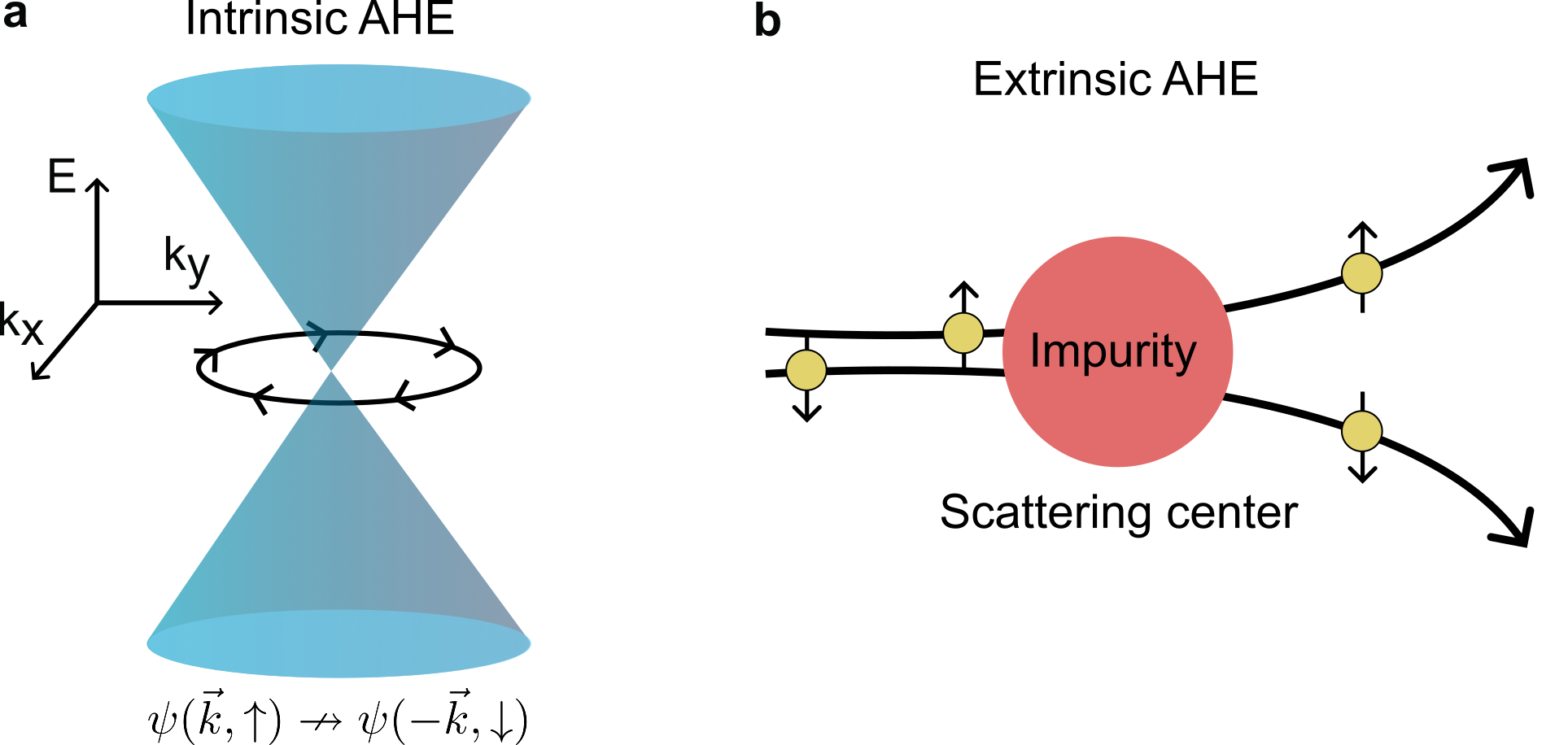
Introduction.—The Anomalous Hall Effect (AHE) was discovered by Edwin Hall only a year after his discovery of the ordinary Hall Effect. However, unlike the classical Hall effect that was immediately rationalized, the mechanism for AHE remained the subject of debate for nearly a century. Today, it is believed that AHE has two types of contributions AHEreview ; AHEreview2 : an intrinsic, scattering-free, mechanism originally proposed by Karplus and Luttinger KarplusLuttinger that can also be reconciled with the presence of a Berry curvature (see Fig. 1a), as well as scattering-dependent mechanisms known as extrinsic contributions (see Fig. 1b). Despite these advances in the 1950s, AHE remains poorly understood in certain systems such as, for example, spin glasses. Notably with the recent emergence of topologically non-trivial band structures, the study and understanding of AHE in these materials led to a renaissance of interest in the topic.
Bismuth is the heaviest group V element () and has therefore a very large atomic spin-orbit coupling (SOC)SOC ; Hofmann . However, due to inversion symmetry in the bulk Bi crystal, the bulk itinerant carriers do not experience SOC, in contrast to the surface state carriers. Bismuth in the bulk form has been extensively studied and has a long history of exhibiting celebrated transport properties. Remarkably, effects such as the Shubnikov-de Haas (SdH) effect, the de Haas-van Alphen effect and the Nernst–Ettingshausen effect were first discovered in bismuth. Recently, in part due to the discovery of graphene, interest in bismuth has been revived for its predicted properties in thin layered structures and in its 2D form known as bismuthene. For instance, a semimetal to semiconductor transition is predicted to occur when its thickness reaches 30 nm or less quantumEffectSsandomirskii ; smsc ; ultrathinBi , but finding such transition has been proven to be experimentally difficult due to fabrication challenges and the potentially non-trivial contribution of surface states Hofmann . Yet, quantum confinement is important in understanding transport properties of films of thickness up to about 100 nmXiao_2012 ; Marcano_2010 ; Jiang_2022 . Furthermore, advances were made in isolating the single layer allotrope, bismuthene, and it was successfully grown for the first time on a SiC substrate in 2017 bismutheneSHE , albeit its transport properties still await to be unraveled experimentally. More recently, there has been a widespread interest in bismuth as there is substantial evidence for it to be a higher order topological insulator (HOTI) HOTI1 ; HOTI2 and to host intrinsic superconductivity where the transition occurs below mK SC . As such, this makes bismuth an excellent candidate to study AHE in a system that is topologically non-trivial.
If time-reversal symmetry (TRS) is broken in bismuth, then one would expect it to manifest the intrinsic AHE AHEreview ; AHEreview2 . For instance, the work of Y. Hirai et al. on 30 nm bismuth film experimentally demonstrated that circularly polarized light can open a gap in the bismuth’s band structure, leading to time-reversal symmetry breaking which then leads to an AHE AHEbismuthlight . Moreover, in a model proposed by Haldane in 1988, he argues that TRS breaking on a honeycomb lattice can lead to a Quantum Anomalous Hall Effect (QAHE) haldane . QAHE was first observed by Chang et al. QAHEfirst in 2013, and in 2018 A. Young et al. QAHEtblg experimentally found QAHE in twisted bilayer graphene where TRS was broken when the interlayer twist angle in the moiré pattern is . Here, we report on our work in sub-100 nm bismuth films whereby an unambiguous signature of the AHE was observed in electronic transport measurements. Bismuth is known to be a diamagnetic material and as such the manifestation of AHE requires the breaking of TRS which is to our knowledge unexpected. Our observation of the AHE in pure bismuth suggests that a hidden mechanism must be responsible for the TRS breaking. This discovery is not only important to further understand the already extensively studied properties of bismuth, but also to extend our comprehension of the AHE.
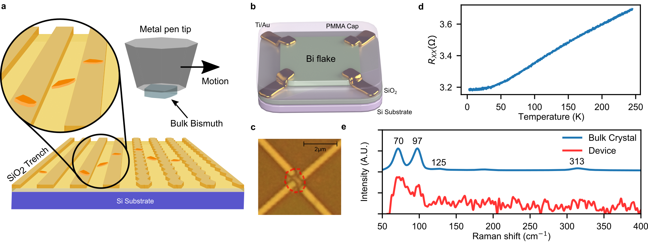
Method.— We developed a novel technique using micro-trench structure to mechanically exfoliate thin bismuth flakes methodpaper . The micro-trench structure was prepared by etching a SiO2 thermal oxide layer above a degenerately doped silicon substrate, effectively turning it to a mechanical file. As shown in Fig. 2a, bulk bismuth crystal, with its orientation carefully chosen to be the (1,1,1) surface, was attached to the tip of a metal pen. By grating the bismuth crystal against the micro-trench file, thin flakes of bismuth were obtained and found to be as thin as 10 nanometers methodpaper . Such mechanical exfoliation provides a way to obtain ultra-thin bismuth flakes in a clean and controlled environment. In particular, compared to the recently reported exfoliation methods using liquid sonication liquidex1 ; liquidex2 , water and oxygen that are detrimental to electronic properties can be avoided. While molecular beam epitaxy (MBE) techniques can produce films down to 3 nm dresselhaus , our method is far more straightforward to prepare high quality flakes down to comparable thicknesses.
Thin bismuth flakes with average thicknesses of 29 to 69 nm were obtained and characterized by atomic force microscopy (AFM), see Supplemental Information. Note that the flakes have height variations, and only the average height is quoted here. Ti/Au contacts were deposited via electron beam lithography (EBL) and electron beam vapor deposition. Note that the environment was carefully controlled with all fabrication steps performed in a vacuum, or in a nitrogen-filled glovebox. Lastly, a polymethyl methacrylate (PMMA) capping layer was spincoated for protecting the bismuth flake against oxidization. An optical image of a 68 nm device (see Supplemental Information) fabricated in the van der Pauw (vdP) geometry is shown in Fig. 2c, with the schematic shown in Fig. 2b. Two other devices fabricated in a comb geometry are shown in the Supplemental Information. Note that due to the small size of the flake ( ), as we will discuss below, the ohmic contacts are subject to misalignments and hence mixing of electronic transport components is to be expected.
The chemical nature of bismuth flakes was confirmed via Raman spectroscopy with a Bruker Senterra confocal Raman equipped with a 785 nm laser. The flake was compared to its bulk counterpart of the same crystal as a benchmark. The small Raman signal of the flake is due to its small size, however it was still possible to observe the 70 cm-1 and 97 cm-1 Raman shift peaks associated with pure bismuth ramanBi1 ; ramanBi2 , see Fig. 2e (red). Additionally, the most common type of bismuth oxide typically formed at lower temperatures (300∘C), -Bi2O3, was observed in the bulk crystal (blue) at 125 cm-1 and 313 cm-1 ramanBioxide1 ; ramanBioxide2 ; ramanBioxide3 but not in the exfoliated flake.
The temperature dependence of the resistance of the van der Pauw device is plotted in Fig. 2d from 3 to 250 K, and is consistent with previously reported values for bulk semi-metallic bismuth kukkonen ; hoffman as well as thin films down to 500 nm partin .
Results and Discussions.— The small size and the limitation imposed by EBL resulted in the van der Pauw contacts to be deposited relatively close to each other, as can be seen in Fig. 2c. Since the contacts are not exactly at the corners as depicted in Fig. 2b, the longitudinal (XX) and Hall (XY) resistances are expected to be mixed to some degree in every probe configuration. To overcome this mixing, we use the Onsager symmetrization to reconstruct the true longitudinal and Hall resistances. According to the Onsager’s reciprocity theorem onsager , inverting the current and voltage contacts in a linear system allows us to measure the transpose of the resistance tensor given by
where is the applied magnetic field. Consequently, by measuring the resistance in one configuration as well as its Onsager reciprocal, the true longitudinal and Hall resistances can be obtained by respectively symmetrizing and anti-symmetrizing the two configurations with
where and form an Onsager pair. For example, a four-point measurement configuration labeled ABCD (corresponding to probes I+/V+/V-/I-) would have its Onsager reciprocal with contact configuration BADC.
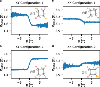
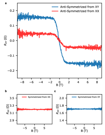
The resistances versus magnetic fields (with positive field defined as pointed into the page, see Fig. 3 insets) were measured at 15 mK and are shown in Fig. 3. We stress that mixing of the and was inevitably observed, however Fig. 3a and Fig. 3b are XY configurations that maximize the Hall signal and that are also Onsager reciprocals to one another. Similarly, Fig. 3c and Fig. 3d are the XX configurations that optimize the XX signal while also capturing a mixed Hall signal. The corresponding ideal probe configurations in the van der Pauw geometry are shown in the insets of Fig. 3.
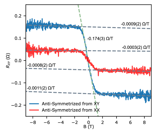
Figure 4 summarizes our main result: the extracted true Hall and longitudinal resistances as a function of the magnetic field . Figure 4a shows the anti-symmetrized signal from the XY configurations, and as expected it is greater than the anti-symmetrized signal from the XX configurations. Similarly, the true longitudinal signal symmetrized in a similar fashion is shown in Fig. 4b and Fig. 4c for the XX and XY configuration pairs, respectively. In particular, both true are constant as a function the magnetic field up to T. The resistance values are 3.2 (extracted from XX) and 1.7 (extracted from XY). The difference in the extracted resistances is attributed to the contacts that are not equidistant from one another, as the ratio of the resistances is approximately equal to the ratio of the distances between the voltage probes.
From the Hall response shown in Fig. 4a, careful inspection of the data shows the presence of a very small slope in the saturated regime of the Hall signal. In particular, for the XY configuration’s saturated high-field region ( T), a fit to the linear slope yields the value , and similarly a linear fit to the XY configuration’s low field region ( T) yields a slope of , see Supplemental Information for the detailed extraction of these values. While the negative values found for both linear Hall signals support the electronic transport being hole-dominated, it is unfortunately not possible to reliably extract carrier densities and mobilities because the constancy of the shown in Fig. 4(a) and (b) is uncharacteristic of the multi-carrier model. Bismuth is known to host both electron and hole pockets in the bulk electronholebismuth ; densitymobilitybismuth , as well as in thin films densitymobilitybismuthfilm ; qconfinement ; magnetotransportbismuth . If both carriers were present, can only saturate at high fields if the densities of electrons and holes were unequal, i.e. . The characteristic field for this saturation is given by magnetoRBi
where and are electron and hole densities, and and are electron and hole mobilities. Note that the reduced Hall slope observed at high fields in Fig. 4(a) implies that which leads to a very high saturation field for . Under such saturation, would have a magnetic field dependence , and if is dominated by a low density, high mobility carrier at low fields, it would have a magnetic field dependence . Neither of these are observed in our work. Carrier density in bismuth can also have a field dependent effect zhu1 ; magnetoRBi ; iwasa , but the linearity of with at high field implies that density variation is not responsible for the observations made here. Moreover, the elongated Fermi surface pockets known for bulk bismuth Hofmann can strongly affect the transport behavior. That being said, the multi-carrier model discussed above is valid as long as the Fermi surfaces are closed. Meanwhile, the possibility of an open orbit in the Fermi surface can be excluded because it is inconsistent with the saturation of at high field as observed in our experiments. All things considered, we cannot reconcile the multi-carrier model with the Hall and magnetotransport data presented in this work. Furthermore, in contrast to bulk bismuth where quantum oscillations can be observed well under 1 T sdhbismuth , in our case we did not observe any SdH oscillations in the longitudinal resistance. As we will discuss below, this unexpected behaviour was nevertheless observed previously in a 100 nm thick film grown by MBE partin .
Using the device geometry and the longitudinal resistance measured in the absence of a magnetic field, the conductivity is calculated to be which places the bismuth device in a good-metal regime dominated by scattering-independent mechanisms AHEreview . It is indeed expected for bismuth to manifest the intrinsic AHE AHEreview ; AHEreview2 because of its high SOC. However, TRS breaking is a necessary condition for both intrinsic and extrinsic AHE, and as such, SOC alone is not sufficient to explain the AHE signal observed here. Usually, intrinsic TRS breaking is achieved by ferro- or antiferromagnetism, but bulk bismuth is known to be the most diamagnetic element with a magnetic susceptibility value of bismuthsusceptibility . Consequently, unless a magnetic transition would occur as the thickness of bismuth is reduced, TRS breaking must originate from elsewhere. Interestingly, in their growth and characterization of bismuth thin films by MBE, Partin et al. found a Hall resistivity and magnetoresistivity nearly identical to our data for their thinnest 100 nm bismuth film (see Fig. 6 of partin ). Specifically, their magnetoresistivity in the 100 nm film was found to be independent of the magnetic field and the Hall resistivity shows a similar AHE behaviour with a saturation near 1 T, as is observed in our work. Importantly, the work of Partin et al. found more conventional behavior for films thicker than 100 nm, leading to the observation of SdH oscillations which is absent in the 100 nm film even for magnetic fields as high as 17 T. The complete featureless and flat trend observed in their and our works for bismuth of similar thicknesses remains an intriguing mystery.
More recently, B. C. Camargo et al. claimed to have observed the AHE in bulk bismuth but were unable to find the source of the TRS breaking either bismuthbulkAHE0 . A portion of their work was dedicated to eliminate magnetic contamination and superconductivity, and it was concluded that the AHE may arise from the topologically non-trivial surface or hinge states rather than in the bulk. Such arguments align with our observation of the AHE in thin devices with average flake thicknesses of 68 nm (main text), 29 nm and 69 nm (see Supplemental Information). Strikingly, these two other devices were fabricated in a comb geometry, yet the four-probe resistances demonstrated a magnetic field response similar to that of AHE measured in the vdP device presented in the main section of our article. While the longitudinal resistances of the vdP and comb devices were different (2 to 32 ), the anomalous Hall responses were unexpectedly similar (0.1 to 0.4 ), hinting that the observed AHE does not arise from the bulk, but instead from the surface. The resistance’s temperature dependence which is consistent with that of the bulk bismuth down to 500 nm also supports this observation as it suggests that the bulk is measured simultaneously with the surface or hinge states.
Finally, in addition to a non-trivial topology in bismuth HOTI1 ; HOTI2 ; bismutheneSHE ; bismuthtopo , there are also other prospect origins for spontaneous TRS breaking. These include band-flattening as in the case of twisted bilayer graphene, orbital magnetism of Dirac electrons that could arise in bismuth, and strain-induced band distortion bismuthstrain ; grapheneflatband ; graphenestrain that could all lead to a broken TRS. There is a long sequence of works supporting an intrinsic AHE in bismuth. From Conn and Donovan’s work in the late 1940s which found traces of AHE bismtuhbulkAHE1 ; bismuthbulkAHE2 ; bismuthbulkAHE0 , to the recent work by B. C. Camargo for the bulk bismuthbulkAHE0 , as well as our own work in exfoliated bismuth that is consistent with Partin’s MBE-grown 100 nm bismuth thin film, all these works point towards a bona fide intrinsic AHE occurring in bismuth with an unknown origin of broken TRS.
Conclusion.— We successfully fabricated sub-100 nm bismuth devices and studied their electronic transport properties. Its measured Hall resistance is consistent with the Anomalous Hall effect despite bismuth being highly diamagnetic. Our results strongly suggest that there must exist a mechanism for breaking TRS in bismuth which needs to be further investigated and understood. In future works, we expect to explore the Hall anomaly at higher magnetic fields and at different field effect gate voltages to obtain a better understanding of its electronic band structure as well as a more profound comprehension of its predicted non-trivial topology. As such, and in spite of having been one of the most extensively studied materials since the 19 century, bismuth remains a fascinating elemental material that is yet to be fully understood.
Acknowledgment
This work has been supported by the Canadian Institute for Advanced Research, the Canadian Foundation for Innovation, and the Fonds de Recherche du Québec Nature et Technologies. Sample fabrication was carried out at the McGill Nanotools Microfabrication facility and GCM Lab at Polytechnique Montréal. We would like to thank R. Talbot, R. Gagnon, and J. Smeros for technical assistance, M.-H. Bernier for helpful electron-beam lithography discussions, Ion Garate for useful discussions of the theory and finally Y. Wang for 3D drawings of the device. R. Allgayer acknowledges the financial support from the Vanier Canada Graduate Scholarship.
References
- (1) N. Nagaosa, J. Sinova, S. Onoda, A. H. MacDonald, and N. P. Ong, Anomalous Hall effect, Rev. Mod. Phys. 82, 1539 (2010).
- (2) D. Culcer, The Anomalous Hall Effect, arXiv:2204.02434, (2020).
- (3) R, Karplus and J. M. Luttinger, Hall Effect in Ferromagnetics, Phys. Rev. 95, 1154 (1954).
- (4) Ph. Hofmann, The surfaces of bismuth: Structural and electronic properties, Prog. Surf. Sci. 81, 191-245 (2006).
- (5) X Gonze, J-P Michenaud, and J-P Vigneron, Ab initio calculations of bismuth properties, including spin–orbit coupling, Phys. Scr. 37, 785 (1988).
- (6) V. B. Sandomirskiǐ, Quantum Size Effect in a Semimetal Film, Soviet Physics JETP 25, 101 (1967).
- (7) C.A. Hoffman, J.R. Meyer, F.J. Bartoli, A. Di Venere, X.J. Yi, C.L. Hou, H.C. Wang, J.B. Ketterson, and G.K. Wong, Semimetal-to-semiconductor transition in bismuth thin films, Phys. Rev. B 48, 11431 (1993).
- (8) T. Hirahara, T. Shirai, T. Hajiri, M. Matsunami, K. Tanaka, S. Kimura, S. Hasegawa, and K. Kobayashi, Role of Quantum and Surface-State Effects in the Bulk Fermi-Level Position of Ultrathin Bi Films, Phys. Rev. Lett. 115, (2015).
- (9) Shunhao Xiao, Dahai Wei, and Xiaofeng Jin, Bi(111) Thin Film with Insulating Interior but Metallic Surfaces, Phys. Rev. Lett. 109, 166805 (2012).
- (10) N. Marcano, S. Sangiao, C. Magén, L. Morellón, M. R. Ibarra, M. Plaza, L. Pérez, and J. M. De Teresa, Role of the surface states in the magnetotransport properties of ultrathin bismuth films, Phys. Rev. B 82, 125326 (2010).
- (11) Zijian Jiang, V. Soghomonian, and J. J. Heremans, Carrier properties of Bi(111) grown on mica and Si(111), Phys. Rev. Materials 6, 095003 (2022).
- (12) F. Reis, G. Li, L. Dudy, M. Bauernfeind, S. Glass, W. Hanke, R. Thomale, J. Schäfer, and R. Claessen, Bismuthene on a SiC substrate: A candidate for a high-temperature quantum spin Hall material, Science 357, 287-290 (2017).
- (13) L. Aggarwal, P. Zhu, T. L. Hughes, and V. Madhavan, Evidence for higher order topology in Bi and Bi0.92Sb0.08, Nat. Comm. 12, (2021).
- (14) F. Schindler, Z. Wang, M. G. Vergniory, A. M. Cook, A. Murani, S. Sengupta, A. Yu. Kasumov, R. Deblock, S. Jeon, I. Drozdov, H. Bouchiat, S. Guéron, A. Yazdani, B. A. Bernevig, and T. Neupert, Higher-order topology in bismuth, Nat. Phys. 14, 918–924 (2018).
- (15) O. Prakash, A. Kumar, A. Thamizhavel, and S. Ramakrishnan, Evidence for bulk superconductivity in pure bismuth single crystals at ambient pressure, Science 335, 52-55 (2017).
- (16) Y. Hirai, N. Yoshikawa, M. Kawaguchi, M. Hayashi, S. Okumura, T. Oka, and R. Shimano, Anomalous Hall effect of light-driven three-dimensional Dirac electrons in bismuth, arXiv:2301.06072, (2023).
- (17) F. D. M. Haldane, Model for a Quantum Hall Effect without Landau Levels: Condensed-Matter Realization of the “Parity Anomaly”, Phys. Rev. Lett. 61, 2015 (1988).
- (18) C.-Z. Chang, J. Zhang, X. Feng, J. Shen, Z. Zhang, M. Guo, K. Li, Y. Ou, P. Wei, L.-L. Wang, Z.-Q. Ji, Y. Feng, S. Ji, X. Chen, J. Jia, X. Dai, Z. Fang, S.-C. Zhang, K. He, Y. Wang, L. Lu, X.-C. Ma, and Q.-K. Xue, Experimental Observation of the Quantum Anomalous Hall Effect in a Magnetic Topological Insulator, Science 340, 167–170 (2013).
- (19) M. Serlin, C. L. Tschirhart, H. Polshyn, Y. Zhang, J. Zhu, K. Watanabe, T. Taniguchi, K. Balents, and A. F. Young, Intrinsic quantized anomalous Hall effect in a moiré heterostructure, Science 367, 900-903 (2019).
- (20) Oulin Yu, R. Allgayer, S. Godin, J. Lalande, P. Fossati, Chunwei Hsu, T. Szkopek, and G. Gervais, Method of Mechanical Exfoliation of Bismuth with Micro-Trench Structures, J. Appl. Phys. 134, 244302 (2023).
- (21) M. Ozhukil Valappil, A. Ganguly, J. Benson, V.K. Pillai, S. Alwarappan, and P. Papakonstantinou, Bismuthene nanosheets produced by ionic liquid assisted grinding exfoliation and their use for oxygen reduction reaction, RSC Adv. 10, 43585 (2020).
- (22) B. Yang, X. Li, Y. Cheng, S. Duan, B. Zhao, W. Yi, C. Wang, H. Sun, Z. Wang, D. Gu, S. Chen, and X. Liu, Liquid phase exfoliation of bismuth nanosheets for flexible all-solid-state supercapacitors with high energy density, J. Mater. Chem. C 8, 12314 (2020).
- (23) E.I. Rogacheva, S.N. Grigorov, O.N. Nashchekina, S. Lyubchenko, and M.S. Dresselhaus, Quantum-size effects in n-type bismuth thin films, Appl. Phys. Lett. 82, 2628–2630 (2003).
- (24) C. Rodriguez-Fernandez, K. Akius, M. Morais de Lima, Andres Cantarero, J. M. van Ruitenbeek, and C. Sabater, Raman signal reveals the rhombohedral crystallographic structure in ultra-thin layers of bismuth thermally evaporated on amorphous substrate, Materials Science & Engineering B 270, 115240 (2021).
- (25) E. S. Walker, S. R. Na, D. Jung, S. D. March, J.-S. Kim, T. Trivedi, W. Li, L. Tao, M. L. Lee, K. M. Liechti, D. Akinwande, S. R. Bank, Large-Area Dry Transfer of Single-Crystalline Epitaxial Bismuth Thin Films, Nano Lett 16, 6931–6938 (2016).
- (26) F. D. Hardcastle and I. E. Wachs, The molecular structure of bismuth oxide by Raman spectroscopy, J. Solid State Chem. 97, 319-331 (1992).
- (27) A. J. Salazar-Pérez, M. A. Camacho-Lopez, R. A. Morales-Luckie, V. Sanchez-Mendieta, F. Urena-Nunez, and J. Arenas-Alatorre, Structural evolution of Bi2O3 prepared by thermal oxidation of bismuth nano-particles, Superficies y Vacio 18, (2005).
- (28) J. A. Steele and R. A. Lewis, In situ micro-Raman studies of laser-induced bismuth oxidation reveals metastability of -Bi2O3 microislands, Opt. Mater. Express 4, 2133-2142 (2014).
- (29) C. A. Kukkonen and K. F. Sohn, The Low-Temperature Electrical Resistivity of Bismuth, J. Phys. F: Met. Phys. 7, L193 (1977).
- (30) R. A. Hoffman and D. R. Frankl, Electrical Transport Properties of Thin Bismuth Films, Phys. Rev. B 3, 1825 (1971).
- (31) D. L. Partin, J. Heremans, D. T. Morelli, C. M. Thrush, C. H. Olk, and T. A. Perry, Growth and Characterization of Epitaxial Bismuth Films, Phys. Rev. B 38, 3818 (1988).
- (32) H. H. Sample, W. J. Bruno, S. B. Sample, and E. K. Sichel, Reverse‐field reciprocity for conducting specimens in magnetic fields, J. of Appl. Phys. 61, 1079-1084 (1987).
- (33) A. L. Jain and S. H. Koenig, Electrons and Holes in Bismuth, Phys. Rev. 127, (1962).
- (34) A. L. Jain, S. K. Suri, and K. Tanaka, Charge carrier densities and mobilities in bismuth, Phys. Lett. A 28, 435-436 (1968).
- (35) S. Kochowski and A. Opilski, Concentration and mobility of charge carriers in thin polycrystalline films of bismuth, Thin Solid Films 48, 345-351 (1978).
- (36) F. Gity, L. Ansari, M. Lanius, P. Schüffelgen, G. Mussler, D. Grützmacher, and J. C. Greer, Reinventing solid state electronics: Harnessing quantum confinement in bismuth thin films, Appl. Phys. Lett. 110, 093111 (2017).
- (37) Y. Zabila, M. Marszalek, M. Krupinski, A. Zarzychi, and M. Perzanowski, Magnetotransport Properties of Semi-Metallic Bismuth Thin Films for Flexible Sensor Applications, Coatings 11, 175 (2021).
- (38) Z. Zhu, B. Fauqué, K. Behnia, and Y. Fuseya, Magnetoresistance and valley degree of freedom in bulk bismuth, J. Phys.: Condens. Matter 30, 313001 (2018).
- (39) Z. Zhu, J. Wang, H. Zuo, B. Fauqué, R.D. McDonald, Y. Fuseya, and K. Behnia, Emptying Dirac valleys in bismuth using high magnetic fields, Nat Commun. 8, 15297 (2017).
- (40) A. Iwasa, A. Kondo, S. Kawachi, K. Akiba, Y. Nakanishi, M. Yoshizawa, M. Tokunaga, and K. Kindo, Thermodynamic evidence of magnetic-field-induced complete valley polarization in bismuth, Sci. Rep. 9, 1672 (2019).
- (41) L. S. Lerner, Shubnikov-de Haas Effect in Bismuth, Phys. Rev. 127, 1480 (1962).
- (42) S. Otake, M. Momiuchi, and N. Matsuno, Temperature Dependence of the Magnetic Susceptibility of Bismuth, J. Phys. Soc. Jpn. 49, 1824 (1980).
- (43) B. C. Camargo, P. Gierłowski, A. Alaferdov, I. N. Demchenko, M. Sawicki, K. Gas, and Y. Kopelevich, Anomalous Hall effect in bismuth, J. Magn. Magn. Mater. 525, 167581 (2021).
- (44) M.-Y. Yao, F. Zhu, C. Q. Han, D. D. Guan, C. Liu, D. Qian, and J.-F. Jia, Topologically nontrivial bismuth(111) thin films, Sci. Rep. 6, 21326 (2016).
- (45) M.-Y. Liu, Y. Huang, Q.-Y. Chen, Z.-Y. Li, C. Cao, and Y. He, Strain and electric field tunable electronic structure of buckled bismuthene, RSC Adv. 7, (2017).
- (46) B. Roy and V. Juricic, Unconventional superconductivity in nearly flat bands in twisted bilayer graphene, Phys. Rev. B 99, 121407(R) (2014).
- (47) C.-C. Hsu, M. L. Teague, J.-Q. Wang, and N.-C. Yeh, Nanoscale strain engineering of giant pseudo-magnetic fields, valley polarization, and topological channels in graphene, Sci. Adv. 6, (2020).
- (48) Donovan and G. T. Conn, LXIX. The electrical conductivity of bismuth fibres: II. Anomalies in the magneto-resistance, The London, Edinburgh, and Dublin Philosophical Magazine and Journal of Science 41, (1950).
- (49) G. T. Conn and B. Donovan, Anomalous Magneto-Resistance Effects in Bismuth, Nature 162, 336 (1948).
Supplemental Material: Anomalous Hall Effect in Thin Bismuth
I Transport Measurements
The resistance of the thin bismuth device was measured with a voltage pre-amplifier using a quasi-DC technique at a frequency of 17.777 Hz and with an excitation current of 100 nA. The low-temperature measurements were performed in a Blufors BF-LD250 dilution refrigerator fitted with a 9 T magnet.
II Temperature Dependence
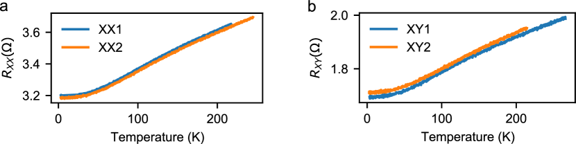
Given that there are four different configurations used in the Onsager symmetrization, we show the resistance versus temperature traces for all of them for completeness. The and are shown in Fig. S1(a) and (b), respectively. Note that the trace for XX2 was shown in the main text of the manuscript.
III Optical Images and AFM Scans
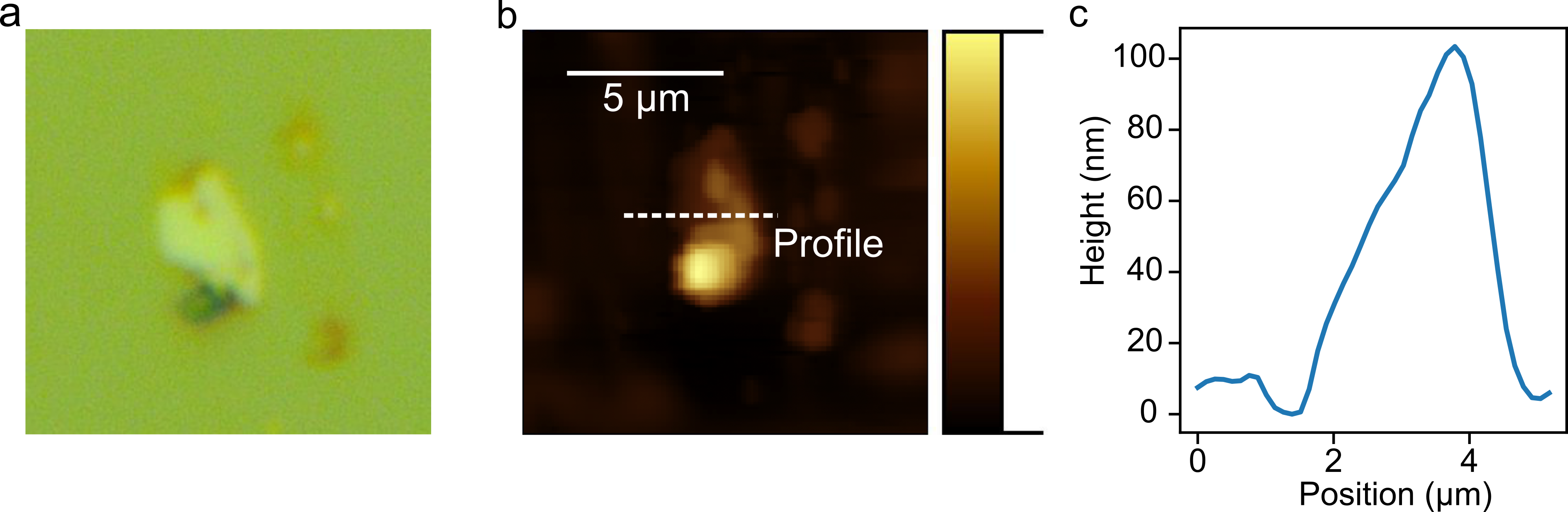
The optical image before contact patterning is shown below in Fig. S2(a). The corresponding AFM scan is shown in Fig. S2(b). A profile is selected across the flake where the height versus position graph is shown in Fig. S2(c). Note that the latter shows a non-negligible height variation, and we found an average height of nm. Despite this height variation, note that we have observed similar AHE in our comb devices (see below) of different thicknesses, and as such we do not expect the unevenness to play an important role in the soundness of our conclusion.
IV Additional Comb Devices
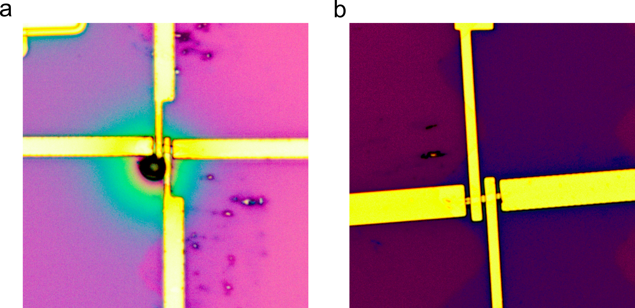
We have observed the Anomalous Hall Effect in two other devices which we label device A and device B. These two devices were fabricated in a comb geometry rather than in a van der Pauw geometry as for the device presented in the main text. We observed the AHE in these two comb devices because of the mixing of transport components due to imperfections in the contacts. The optical images of the devices are shown below in Fig. S3. The thicknesses for devices A and B are nm and nm, respectively. The resistances are 19 and 32 for devices A and B, respectively.
For device A, we present the raw measured four-point resistance versus the magnetic field, shown below in Fig. S4.
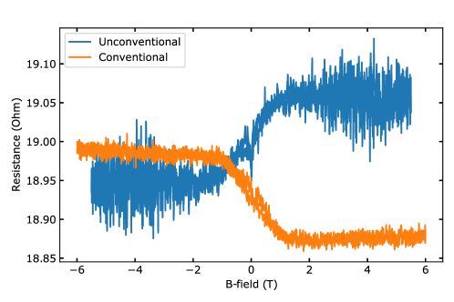
The conventional configuration is the usual I+/V+/V-/I- configuration where the current contacts are on the outside of the comb geometry and the voltage probes are in the center. In contrast, the unconventional configuration is obtained by inverting I+ with V+ and I- with V-. This effectively becomes the Onsager reciprocal of the conventional setup. Although the AHE is clearly observed, the two curves do not cross at the origin which we attribute tentatively to the non-ideal configuration for Hall response used here.
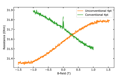
In Fig. S5 below we show the resistance dependence on the magnetic field for device B. Similarly to device A, the AHE is clearly observed despite a vertical offset most likely due to the non-ideal configuration for measuring a Hall response.
V Linear Fits of the Anomalous Hall Response
We perform linear fits on the anti-symmetrized data shown in the main text of the manuscript. The high-field region is chosen to be T and the low field region is chosen as T. The corresponding slopes are shown in Fig. S6.