Scaling on-chip photonic neural processors using
arbitrarily programmable wave propagation
Abstract
On-chip photonic processors for neural networks have potential benefits in both speed and energy efficiency but have not yet reached the scale at which they can outperform electronic processors. The dominant paradigm for designing on-chip photonics is to make networks of relatively bulky discrete components, such as Mach–Zehnder interferometers and microring resonators, connected by one-dimensional waveguides. A far more compact alternative is to avoid explicitly defining any components and instead sculpt the continuous substrate of the photonic processor to directly perform the computation using the multimode interference of waves freely propagating in two dimensions. We propose and demonstrate a device whose refractive index as a function of space, , can be rapidly reprogrammed, allowing arbitrary control over the wave propagation in the device. Our device, a 2D-programmable waveguide, combines photoconductive gain with the electro-optic effect to achieve massively parallel modulation of the refractive index of a slab waveguide, with an index modulation depth of and approximately programmable degrees of freedom. We used a prototype device with a functional area of to perform neural-network inference with up to 49-dimensional input vectors in a single pass, achieving 96% accuracy on vowel classification and 86% accuracy on -pixel MNIST handwritten-digit classification, with no trained digital-electronic pre- or post-processing. This is a scale beyond that of previous photonic chips relying on discrete components, illustrating the benefit of the continuous-waves paradigm.
In principle, with large enough chip area, the reprogrammability of the device’s refractive index distribution enables the reconfigurable realization of any passive, linear photonic circuit or device. This promises the development of more compact and versatile photonic systems for a wide range of applications, including optical processing, smart sensing, spectroscopy, and optical communications.
I Introduction
Deep neural networks (DNNs) have gained widespread adoption across many domains ranging from computer vision to natural language processing [1]. The size of DNN models has been increasing exponentially over the past decade, leading to exponentially increasing energy costs for running them. Limits to energy costs now impose a practical constraint on how large models can be [2, 3], strongly motivating the exploration of alternative, energy-efficient computing approaches for executing DNNs, whose computational cost is typically dominated by that of matrix-vector multiplications (MVMs). Optical neural networks (ONNs) that specialize in performing MVMs with optics instead of electronics are one promising candidate approach [4, 5, 6].
Integrated photonics is a leading platform for optical neural networks due to its compact form factor, excellent phase stability, availability of high-bandwidth modulators and detectors, manufacturability, and ease of integration with electronics [4, 7, 8, 9, 10, 11, 12]. The dominant paradigm for designing integrated photonic neural networks is to construct networks of discrete, programmable photonic components such as Mach–Zehnder interferometers, microring resonators, or phase-change-memory cells, connected by single-mode waveguides. These networks execute a linear-optical operation: a MVM between the vector encoded in the optical input to the chip and the matrix programmed in the discrete components. However, the maximum vector size, , supported by chips using this approach has so far been restricted (see Appendix Table A1) to sizes far below what is necessary for optics to deliver an energy-efficiency advantage () [13, 14, 15, 16]. The scale of such chips has been limited by the large spatial footprint of individual components and the inefficiency of dedicating a substantial portion of the chip’s area to non-programmable interconnection regions comprising well-isolated waveguides that connect relatively sparsely arranged programmable elements***Another important limiting factor has been fabrication imperfections [17, 18], which lead to compounding errors..
If, instead of building the integrated photonic neural network from discrete components, we treated the entire chip as a blank slate that we could arbitrarily and reprogrammably sculpt, we could achieve far greater spatial efficiency [19, 20]. But for the integrated-photonic chip to perform an MVM with a programmable matrix, we need to be able to continuously program the chip’s refractive index distribution, [21, 20, 19, 22, 23, 24]. How can we make a photonic chip whose refractive index distribution is programmable? In conventional nanophotonic chips, is controlled by etching away material in lithographically defined regions—and is fixed at fabrication time. While inversed-designed chips [25] realizing MVMs with fixed matrices can be made [23], we generally would like to be able to program the matrix. Photorefractive crystals were explored several decades ago as a means to implement programmable linear operations with slab waveguides [26, 27], but fell out of favor because the small achievable refractive-index modulation () meant that even centimeter-scale waveguides were unable to perform large-scale operations. Additionally, phase-change materials have recently been demonstrated to realize arbitrary [28, 29], but suffer from slow rewriting speed†††Approximately 3 mm2 per minute in Ref. [29]. This limitation arises because rewriting is performed with a focused laser beam targeting a sub-micron spot, with the beam ultimately rastered across the phase-change-material substrate to modify the entire distribution . and a limited number of rewrite cycles‡‡‡ in Ref. [30].. The scale is also currently limited: Ref. [29] reported programming a device with a 3-dimensional input and a 3-dimensional output.
In this work, we introduce a photonic chip that realizes a two-dimensionally-programmable (2D-programmable) waveguide. The chip uses massively parallel electro-optic modulation to program across 10,000 individual regions of a lithium niobate slab waveguide, and we train multimode photonic structures within the chip that perform neural-network inference (Fig. 1). The structures realized by our 2D-programmable waveguide are similar to inverse-designed nanophotonic devices [25, 23]: they are computer-optimized, two-dimensional metastructures that control multimode wave propagation. A distinguishing feature of our device is its programmability, setting it apart from typical inverse-designed photonic devices, which are fixed after manufacturing. We achieve programmability optically: a pattern of light shone on top of our device creates a refractive-index distribution in the slab waveguide. The programming works as follows: By projecting patterns of light onto a photoconductive film fabricated above the lithium niobate waveguide, we control the quasi-DC electric field distribution, , across it. This in turn induces a refractive-index modulation via the strong electro-optic effect in lithium niobate. With the ability to program any continuous refractive index distribution in 2D, we could in principle program (or learn) any passive photonic circuit, device, or system. Here, however, we focus on performing optical-neural-network calculations, both because this is an application that is well-suited to the analog computation realized by multimode wave propagation, and because it is an application that demands large-scale (i.e., highly multimode), complex photonic transformations. In our work we show how we can train the refractive-index distribution so that wave propagation through the device performs a desired neural-network inference. Our method adapts a hybrid in-silico, in-situ backpropagation algorithm [31] that makes it practical to learn a very large number (10,000) of parameters. A key contribution of our work is to show how to construct and calibrate a physics-informed simulation model of our chip that is sufficiently accurate, even at the scale of 49-dimensional inputs and 10,000 tunable parameters, for gradient-descent training to converge to good solutions. We apply our device to both vowel and MNIST handwritten-digit classification, and perform classifications using just a single pass through the device. This is in contrast to most prior works on neural-network inference with integrated photonics, which use photonic chips that are too small to receive the entire input data vector in a single shot, so require multiple passes. We also do not rely on any trainable digital-electronic pre- or post-processing; the vast majority of the computation is performed from start to finish by our optical apparatus.
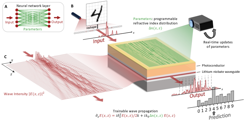
II Operating Principle of the Device
In Fig. 1, we show a conceptual schematic for how to perform machine learning with the 2D-programmable waveguide. We amplitude-encode the machine learning input data into the 1D input-field distribution, , which serves as the initial condition for programmable wave propagation described by the partial differential equation . Here, denotes the propagation direction, the transverse dimension, while and are the wavenumbers in free space and the slab waveguide, respectively. After propagation through the device, we measure the field’s intensity, , at the output facet and bin it to produce the machine learning task’s output vector. The key feature of our device is that we can program the refractive index distribution, , in real-time by projecting patterns of light (shown in green) onto the device. This programmability allows us to train the parameters of the device directly in the laboratory via gradient-based algorithms to perform machine learning tasks.
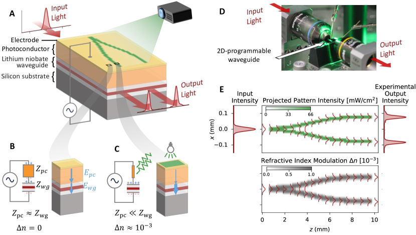
In Fig. 2, we show how patterns of light program the refractive index distribution. Our device, which is inspired by optoelectronic tweezers enabled by photoconductive gain [32, 33], is composed of a lithium niobate slab waveguide and a photoconductive film, which are sandwiched between a pair of electrodes that have an oscillating voltage placed across them (see Fig. 2A). Projecting a light pattern onto the chip creates a spatially varying electric field within the slab waveguide. As shown in Fig. 2B and 2C, this results from the voltage division between the photoconductor and the slab waveguide. For regions of the chip that are illuminated at intensities of tens of , the photoconductor’s impedance drops significantly, increasing the electric field within the slab waveguide. Combined with lithium niobate’s strong electro-optic effect, this spatially varying electric field distribution induces a spatially varying refractive index modulation. In our device, the largest refractive index modulation is approximately , limited by the geometry of the material stack and a safety margin to prevent dielectric breakdown. In principle, it can be improved to , a limit set by lithium niobate’s breakdown field [34]. We note that unlike conventional etched nanophotonic structures, the refractive index modulation in our device can take on continuous values by continuously varying the intensity of the projected pattern. For more details on the device design, including the fabrication procedure, see Appendix A.
Using a digital micromirror device illuminated by an LED, we projected patterns across a area, achieving a pixel resolution of . This configuration enabled us to control the refractive index distribution across 10,000 degrees of freedom (see Appendix D.1) and update the entire distribution at a rate of . To maximize the refractive index modulation, we applied a voltage of across the electrodes. Given that CMOS electrode backplanes can only support spatially programmable voltages of around , our approach of using photoconductive gain is crucial. It allows us to apply a large voltage to a single unpatterned electrode, and realize “virtual electrodes” via the patterned illumination [32, 33]. Finally, the device has a propagation loss of less than at a wavelength of (see Appendix B.3).
To illustrate the operating principle of our device, we projected a pattern in the shape of a Y-branch splitter onto the 2D-programmable waveguide (see Fig. 2A and 2E). Because the refractive index distribution is approximately proportional to the projected pattern , the projected pattern instantiates a refractive index distribution of a Y-branch splitter and thereby splits the input beam into two output beams. We couple a single input Gaussian beam into the device using a beamshaper. This beamshaper allows for the realization of arbitrary input optical fields (up to a spatial resolution of ), a capability we use for our machine learning demonstrations. We then measured the intensity of the output beam with a camera. For further details on the experimental setup, see Appendix C. The experimental results in Fig. 2E show that the input beam is split into two equal output beams, in agreement with the simulated wave propagation.
III Machine learning demonstrations with the 2D-programmable waveguide
In this work, we apply the 2D-programmable waveguide to perform machine learning tasks, specifically focusing on vowel classification [35] and MNIST handwritten digit classification [36]. Both datasets, along with their variations, have been used as a benchmark for similar on-chip optical neural networks, thereby providing useful points of comparison [24, 4, 10].
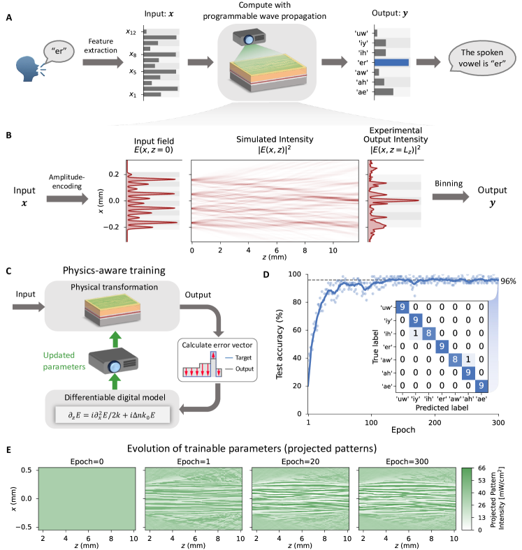
The vowel classification dataset comprises formant frequencies extracted from audio recordings of spoken vowels by various speakers. The task is to predict which of the 7 vowels is spoken, given a 12-dimensional input data vector of formant frequencies. We divided the dataset into a training set and a testing set, comprising 75% (n=196) and 25% (n=63) of the samples, respectively.
In Fig. 3, we present our experimental results on performing vowel classification with the 2D-programmable waveguide. As shown in Fig. 3A and 3B, we encoded the 12-dimensional input vectors into the amplitudes of twelve spatial Gaussian modes (whose mean positions are linearly spaced) at the input facet of the device. This input optical beam produced by the beamshaper undergoes complex wave propagation in the 2D-programmable waveguide. For readout, we measured the intensity at the output facet with a camera, and binned the measurement into seven different regions, with each region corresponding to a specific vowel. The predicted vowel for an input is given by the region that receives the most power. Thus, the refractive index distribution is trained so that the wave propagation directs the most power towards the region corresponding to the correct vowel. For more details on the output decoding and the overall computational model of the ONN demonstrations, see Appendix F.1. As shown in the simulated intensity distribution in Fig. 3B, the device learns to leverage complex multimode wave propagation to perform the neural network inference in a spatially efficient manner.
The refractive index distribution to implement vowel classification is learned using physics-aware training [31], a modified backpropagation algorithm. The hybrid in-situ, in-silico nature of the algorithm allows for efficient training even in the presence of both imperfect models and experimental noise (see Appendix D.3 for more detail). The algorithm requires a digital model of the experiment, which was challenging to construct due to the large number of parameters and the complexity of the wave propagation. Initially, a purely physics-based model (using the PDE governing the wave evolution) provided qualitative but not quantitative agreement with the experimental results. This discrepancy led us to integrate data-driven refinements to the physics-based model, which achieved quantitative agreement with the experiment (see Appendix E for a detailed description of the digital model).
Using physics-aware training, we trained the 2D-programmable waveguide for a total of 300 epochs, which took approximately one hour on the experimental setup (see Fig. 3D). As shown in Fig. 3E, the projected pattern, which is initialized as a uniform illumination, evolves into a complex pattern that is challenging to interpret. These patterns resemble the refractive index distributions found in inverse-designed photonic devices; this is expected as we share the same principle of using computational optimization to design/train the device to perform a desired function. Fig. 3D shows that despite the complexity of the projected pattern, the 2D-programmable waveguide successfully performs the vowel classification task, and achieved a test accuracy of 96% after training.
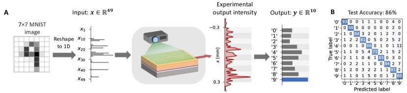
In Fig. 4, we present our experimental results on MNIST handwritten-digit classification. The task consists of 14-by-14 pixel images of handwritten digits from 0 to 9. We divide the MNIST dataset in the standard manner into 60,000 training images and 10,000 test images. We down-sampled MNIST images to 7-by-7 pixels, then flattened them to 49-dimensional vectors.
To train a refractive index pattern to perform MNIST classification, we follow the same procedure used for the vowel classification task (see Fig. 3). Thus, the 2D-programmable waveguide processed the 49-dimensional input vector to produce a 10-dimensional output vector that corresponds to the 10 possible digits (see Appendix F.3 for more details regarding the MNIST results). As shown in Fig. 4B, the system achieved 86% accuracy on the test dataset after 10 epochs of training, which takes about 10 hours on our setup. This falls 4 percentage points short of the 90% accuracy that a one-layer digital neural network achieves on this downsampled MNIST classification task, likely due to imperfect modeling and experimental drifts. Nevertheless, this result demonstrates that complex wave propagation in our device can be harnessed to perform computations comparable to that of a single-layer neural network with a matrix.
IV Discussion
We have introduced and demonstrated a 2D-programmable photonic chip comprising a lithium niobate slab waveguide whose refractive index distribution, we can continuously program. The device design enables programming by massively parallel electro-optic modulation with approximately 10,000 degrees of freedom. We used our chip to perform neural-network inference by training the refractive-index distribution, and consequently the multimode wave propagation through the chip. To train the device, we developed a physics-based model of the chip’s behavior, along with a data-driven refinement allowing the model to be sufficiently accurate that it supports backpropagation-based training [31].
The predominant approach to building integrated photonic neural networks is to fabricate large arrays of discrete components (such as Mach–Zehnder interferometers, microring resonators, or phase-change memories) connected by single-mode waveguides [6]. In contrast, we have adopted the conceptual approach of using wave propagation in distributed spatial modes [27, 21, 20, 19, 22, 37, 23], which can be far more space-efficient [19, 20, 37]. The device we have introduced gives a practical means to realize the vision of neural-network inference using programmable multimode wave propagation. Our prototype chip was able to perform neural-network inference with input vectors of dimension up to 49, which is larger than the capability of neural-network photonic chips reported in Refs. [4, 9, 12, 10, 38, 24] (see Appendix G for a detailed comparison). This large input dimension enabled us to use our chip to perform MNIST handwritten-digit classification with a single pass through the chip, and without using any digital-electronic parameters.
IV.1 Future device improvements
Looking to the future, relatively modest improvements to the device would allow us to realize both wider and deeper neural networks with a single chip. Our current device has a programmable refractive-index modulation of , and the wave propagation takes place in a region measuring wide and long. We show in simulation that increasing each of these device parameters by a factor of five would enable the implementation of arbituary unitary matrices with vector dimensions over a hundred () (see Appendix H.2). In our current work, our chip performs a single-layer neural-network computation (i.e., having a depth of 1). Increasing the depth of the neural network run in a single pass through the chip would require performing nonlinear activation functions on-chip [12, 9, 11]. Given that our chip’s slab waveguide already uses a nonlinear material, lithium niobate, one could periodically pole the lithium niobate in certain regions of the chip, enabling nonlinear interaction between optical waves in those regions, which can be used to engineer all-optical nonlinear activation functions [39]. Alternatively, multilayer computation can be performed by propagation of waves in a continuous nonlinear medium [22, 21, 20], since programmable nonlinear wave propagation can be mathematically mapped to a deep multilayer neural network [22, 21]. A power-efficient realization of this approach in our platform could involve using an appropriately poled lithium niobate slab waveguide with a cascaded second-order nonlinearity [40].
Besides making the device improvements needed to increase the width and depth of the neural networks that are executed in a single pass, there are two other important engineering directions for future work. The throughput of our current demonstration is low, at 25 input vectors per second, limited by the use of a liquid-crystal-based beamshaper for generating inputs, and a slow camera for reading outputs. The throughout could be increased to input vectors per second by replacing the beamshaper with fast on-chip lithium-niobate modulators, and the camera with fast on-chip detectors [41, 42]. We envision that a fully-integrated version of the system could be built by also replacing the current free-space projector setup for programming with a micro-LED display that is directly bonded onto the device (see Appendix H.1 for more detail).
Realizing 2D-programmable waveguide chips with larger refractive-index modulation and larger area will be useful not only for photonic neural networks but also for all other applications where linear-optical transformations are applied on-chip [43]. A weakness of our current demonstration device is the relatively small refractive index modulation () compared to conventional lithographically defined nanophotonics (): the refractive-index modulation one can achieve in any device with our design is ultimately constrained by the material properties of the waveguide core: its electro-optic coefficient and the maximum electric field it can sustain. With lithium niobate, the modulation we measured, , could be improved to by increasing the thickness and improving the material properties of the photoconductor (see Appendix A.3). However, using an alternative electro-optic material for the waveguide, such as barium titanate [44], highly nonlinear polymers [45], or liquid crystals [46], could allow future realizations to achieve a refractive-index modulation of or larger.
IV.2 Future device directions and applications
We have demonstrated control over the real component of the refractive index; the functionality of a 2D-programmable waveguide could be enhanced by combining it with control over the imaginary component of the refractive index (i.e., gain/loss), as was demonstrated separately in complementary recent work [24]. We could also modify the device presented in this current work to realize an arbitrarily programmable nonlinear medium, where the second-order nonlinear optical susceptibility could be programmed in real time. This may be achieved by applying the same operating principle of electric-field programming using photoconductive gain to a waveguide whose core material has a large third-order nonlinearity (such as silicon [47], silicon nitride [48], or tantalum pentoxide [49]), inducing a strong second-order nonlinearity [50].
To conclude, we believe that our device concept, with its ability to programmably control multimode wave propagation, may create new opportunities in the broader fields of optical computing and optical information processing [5, 6, 16]. Although our work in this paper has focused on machine learning, our device could also be used for solving integral equations [51] and combinatorial-optimization problems [52]. Our device could also be used in smart sensing [12, 53] and spectroscopy [54, 55], as well as in optical communications [56, 57, 11]. Even more generally, one can in principle program any passive photonic circuit or structure, continuously fine-tune or adapt that circuit, or even learn in situ a tailored photonic device directly for an application, essentially enabling photonic inverse design that can occur post-fabrication [25]. It may ultimately even be possible to make a device that combines programmability of linear wave propagation (this work), nonlinear wave propagation (a natural extension of this work to realize programmable ), and gain/loss (demonstrated in Ref. [24]), giving rise to an on-chip platform capable of replicating almost every functionality we have in free-space optics.
References
- [1] LeCun, Y., Bengio, Y. & Hinton, G. Deep learning. Nature 521, 436–444 (2015).
- [2] Patterson, D. et al. Carbon emissions and large neural network training. arXiv:2104.10350 (2021).
- [3] Sevilla, J., Heim, L., Ho, A., Besiroglu, T., Hobbhahn, M. & Villalobos, P. Compute trends across three eras of machine learning. In 2022 International Joint Conference on Neural Networks (IJCNN), 1–8 (2022).
- [4] Shen, Y. et al. Deep learning with coherent nanophotonic circuits. Nature Photonics 11, 441–446 (2017).
- [5] Wetzstein, G. et al. Inference in artificial intelligence with deep optics and photonics. Nature 588, 39–47 (2020).
- [6] Shastri, B. J., Tait, A. N., Ferreira de Lima, T., Pernice, W. H., Bhaskaran, H., Wright, C. D. & Prucnal, P. R. Photonics for artificial intelligence and neuromorphic computing. Nature Photonics 15, 102–114 (2021).
- [7] Tait, A. N., de Lima, T. F., Zhou, E., Wu, A. X., Nahmias, M. A., Shastri, B. J. & Prucnal, P. R. Neuromorphic photonic networks using silicon photonic weight banks. Scientific Reports 7 (2017).
- [8] Feldmann, J., Youngblood, N., Wright, C. D., Bhaskaran, H. & Pernice, W. H. All-optical spiking neurosynaptic networks with self-learning capabilities. Nature 569, 208–214 (2019).
- [9] Bandyopadhyay, S. et al. Single chip photonic deep neural network with accelerated training. arXiv:2208.01623 (2022).
- [10] Feldmann, J. et al. Parallel convolutional processing using an integrated photonic tensor core. Nature 589, 52–58 (2021).
- [11] Huang, C. et al. A silicon photonic–electronic neural network for fibre nonlinearity compensation. Nature Electronics 4, 837–844 (2021).
- [12] Ashtiani, F., Geers, A. J. & Aflatouni, F. An on-chip photonic deep neural network for image classification. Nature 606, 501–506 (2022).
- [13] Hamerly, R., Bernstein, L., Sludds, A., Soljačić, M. & Englund, D. Large-scale optical neural networks based on photoelectric multiplication. Physical Review X 9, 021032 (2019).
- [14] Nahmias, M. A., De Lima, T. F., Tait, A. N., Peng, H.-T., Shastri, B. J. & Prucnal, P. R. Photonic multiply-accumulate operations for neural networks. IEEE Journal of Selected Topics in Quantum Electronics 26, 1–18 (2019).
- [15] Anderson, M. G., Ma, S.-Y., Wang, T., Wright, L. G. & McMahon, P. L. Optical transformers. arXiv:2302.10360 (2023).
- [16] McMahon, P. L. The physics of optical computing. Nature Reviews Physics 5, 717–734 (2023).
- [17] Chrostowski, L., Wang, X., Flueckiger, J., Wu, Y., Wang, Y. & Fard, S. T. Impact of fabrication non-uniformity on chip-scale silicon photonic integrated circuits. In Optical Fiber Communication Conference, Th2A–37 (Optica Publishing Group, 2014).
- [18] Burgwal, R., Clements, W. R., Smith, D. H., Gates, J. C., Kolthammer, W. S., Renema, J. J. & Walmsley, I. A. Using an imperfect photonic network to implement random unitaries. Optics Express 25, 28236–28245 (2017).
- [19] Larocque, H. & Englund, D. Universal linear optics by programmable multimode interference. Optics Express 29, 38257–38267 (2021).
- [20] Khoram, E., Chen, A., Liu, D., Ying, L., Wang, Q., Yuan, M. & Yu, Z. Nanophotonic media for artificial neural inference. Photonics Research 7, 823–827 (2019).
- [21] Hughes, T. W., Williamson, I. A. D., Minkov, M. & Fan, S. Wave physics as an analog recurrent neural network. Science Advances 5, eaay6946 (2019).
- [22] Nakajima, M., Tanaka, K. & Hashimoto, T. Neural Schrödinger equation: Physical law as deep neural network. IEEE Transactions on Neural Networks and Learning Systems 33, 2686–2700 (2022).
- [23] Nikkhah, V., Pirmoradi, A., Ashtiani, F., Edwards, B., Aflatouni, F. & Engheta, N. Inverse-designed low-index-contrast structures on a silicon photonics platform for vector–matrix multiplication. Nature Photonics (2024).
- [24] Wu, T., Menarini, M., Gao, Z. & Feng, L. Lithography-free reconfigurable integrated photonic processor. Nature Photonics 17, 710–716 (2023).
- [25] Molesky, S., Lin, Z., Piggott, A. Y., Jin, W., Vucković, J. & Rodriguez, A. W. Inverse design in nanophotonics. Nature Photonics 12, 659–670 (2018).
- [26] Psaltis, D., Brady, D., Gu, X.-G. & Lin, S. Holography in artificial neural networks. Nature 343, 325–330 (1990).
- [27] Brady, D. J. & Psaltis, D. Holographic interconnections in photorefractive waveguides. Applied Optics 30, 2324 (1991).
- [28] Delaney, M. et al. Nonvolatile programmable silicon photonics using an ultralow-loss Sb2Se3 phase change material. Science Advances 7, eabg3500 (2021).
- [29] Wu, C., Deng, H., Huang, Y.-S., Yu, H., Takeuchi, I., Ríos Ocampo, C. A. & Li, M. Freeform direct-write and rewritable photonic integrated circuits in phase-change thin films. Science Advances 10, eadk1361 (2024).
- [30] Delaney, M., Zeimpekis, I., Lawson, D., Hewak, D. W. & Muskens, O. L. A new family of ultralow loss reversible phase‐change materials for photonic integrated circuits: and . Advanced Functional Materials 30, 2002447 (2020).
- [31] Wright, L. G., Onodera, T., Stein, M. M., Wang, T., Schachter, D. T., Hu, Z. & McMahon, P. L. Deep physical neural networks trained with backpropagation. Nature 601, 549–555 (2022).
- [32] Chiou, P. Y., Ohta, A. T. & Wu, M. C. Massively parallel manipulation of single cells and microparticles using optical images. Nature 436, 370–372 (2005).
- [33] Wu, M. C. Optoelectronic tweezers. Nature Photonics 5, 322–324 (2011).
- [34] Luennemann, M., Hartwig, U., Panotopoulos, G. & Buse, K. Electrooptic properties of lithium niobate crystals for extremely high external electric fields. Applied Physics B 76, 403–406 (2003).
- [35] Hillenbrand, J., Getty, L. A., Clark, M. J. & Wheeler, K. Acoustic characteristics of american english vowels. The Journal of the Acoustical society of America 97, 3099–3111 (1995).
- [36] LeCun, Y. The MNIST database of handwritten digits. http://yann. lecun. com/exdb/mnist/ (1998).
- [37] Gu, J., Zhu, H., Feng, C., Jiang, Z., Chen, R. T. & Pan, D. Z. M3icro: Machine learning-enabled compact photonic tensor core based on programmable multi-operand multimode interference. arXiv:2305.19505 (2023).
- [38] Huang, C. et al. Demonstration of scalable microring weight bank control for large-scale photonic integrated circuits. APL Photonics 5 (2020).
- [39] Li, G. H., Sekine, R., Nehra, R., Gray, R. M., Ledezma, L., Guo, Q. & Marandi, A. All-optical ultrafast ReLU function for energy-efficient nanophotonic deep learning. Nanophotonics 12, 847–855 (2022).
- [40] Cui, C., Zhang, L. & Fan, L. In situ control of effective Kerr nonlinearity with Pockels integrated photonics. Nature Physics 18, 497–501 (2022).
- [41] Wang, C. et al. Integrated lithium niobate electro-optic modulators operating at CMOS-compatible voltages. Nature 562, 101–104 (2018).
- [42] Ahn, G. H. et al. Platform-agnostic waveguide integration of high-speed photodetectors with evaporated tellurium thin films. Optica 10, 349 (2023).
- [43] Bogaerts, W. et al. Programmable photonic circuits. Nature 586, 207–216 (2020).
- [44] Tang, P., Meier, A. L., Towner, D. J. & Wessels, B. W. BaTiO3 thin-film waveguide modulator with a low voltage–length product at near-infrared wavelengths of 098 and 155 µm. Optics Letters 30, 254 (2005).
- [45] Koeber, S. et al. Femtojoule electro-optic modulation using a silicon–organic hybrid device. Light: Science & Applications 4, e255 (2015).
- [46] Davis, S. R., Farca, G., Rommel, S. D., Johnson, S. & Anderson, M. H. Liquid crystal waveguides: new devices enabled by 1000 waves of optical phase control. In Emerging Liquid Crystal Technologies V, vol. 7618, 76180E. International Society for Optics and Photonics (SPIE, 2010).
- [47] Leuthold, J., Koos, C. & Freude, W. Nonlinear silicon photonics. Nature Photonics 4, 535–544 (2010).
- [48] Blumenthal, D. J., Heideman, R., Geuzebroek, D., Leinse, A. & Roeloffzen, C. Silicon nitride in silicon photonics. Proceedings of the IEEE 106, 2209–2231 (2018).
- [49] Jung, H., Yu, S.-P., Carlson, D. R., Drake, T. E., Briles, T. C. & Papp, S. B. Tantala Kerr nonlinear integrated photonics. Optica 8, 811 (2021).
- [50] Timurdogan, E., Poulton, C. V., Byrd, M. J. & Watts, M. R. Electric field-induced second-order nonlinear optical effects in silicon waveguides. Nature Photonics 11, 200–206 (2017).
- [51] Mohammadi Estakhri, N., Edwards, B. & Engheta, N. Inverse-designed metastructures that solve equations. Science 363, 1333–1338 (2019).
- [52] Roques-Carmes, C. et al. Heuristic recurrent algorithms for photonic ising machines. Nature Communications 11, 249 (2020).
- [53] Yamaguchi, T., Arai, K., Niiyama, T., Uchida, A. & Sunada, S. Time-domain photonic image processor based on speckle projection and reservoir computing. Communications Physics 6, 250 (2023).
- [54] Yao, C., Xu, K., Zhang, W., Chen, M., Cheng, Q. & Penty, R. Integrated reconstructive spectrometer with programmable photonic circuits. Nature Communications 14, 6376 (2023).
- [55] Yang, Z., Albrow-Owen, T., Cai, W. & Hasan, T. Miniaturization of optical spectrometers. Science 371, eabe0722 (2021).
- [56] Cheng, Q., Rumley, S., Bahadori, M. & Bergman, K. Photonic switching in high performance datacenters. Optics express 26, 16022–16043 (2018).
- [57] Yang, K. Y. et al. Multi-dimensional data transmission using inverse-designed silicon photonics and microcombs. Nature Communications 13, 7862 (2022).
- [58] Habermehl, S., Apodaca, R. T. & Kaplar, R. J. On dielectric breakdown in silicon-rich silicon nitride thin films. Applied Physics Letters 94, 012905 (2009).
- [59] Piccirillo, A. & Gobbi, A. L. Physical‐electrical properties of silicon nitride deposited by PECVD on III–V semiconductors. Journal of The Electrochemical Society 137, 3910–3917 (1990).
- [60] Srivastava, J. K., Prasad, M. & Wagner, J. B. Electrical conductivity of silicon dioxide thermally grown on silicon. Journal of The Electrochemical Society 132, 955–963 (1985).
- [61] Janotta, A. et al. Doping and its efficiency in . Phys. Rev. B 69, 115206 (2004).
- [62] Piccoli, G., Sanna, M., Borghi, M., Pavesi, L. & Ghulinyan, M. Silicon oxynitride platform for linear and nonlinear photonics at nir wavelengths. Optical Materials Express 12, 3551 (2022).
- [63] Ghatak, A., Thyagarajan, K. & Shenoy, M. Numerical analysis of planar optical waveguides using matrix approach. Journal of Lightwave Technology 5, 660–667 (1987).
- [64] Zhang, M., Wang, C., Cheng, R., Shams-Ansari, A. & Lončar, M. Monolithic ultra-high-Q lithium niobate microring resonator. Optica 4, 1536 (2017).
- [65] Bender, N., Yamilov, A., Goetschy, A., Yılmaz, H., Hsu, C. W. & Cao, H. Depth-targeted energy delivery deep inside scattering media. Nature Physics 18, 309–315 (2022).
- [66] Frumker, E. & Silberberg, Y. Phase and amplitude pulse shaping with two-dimensional phase-only spatial light modulators. JOSA B 24, 2940–2947 (2007).
- [67] Hughes, T. W., Minkov, M., Shi, Y. & Fan, S. Training of photonic neural networks through in situ backpropagation and gradient measurement. Optica 5, 864–871 (2018).
- [68] Pai, S. et al. Experimentally realized in situ backpropagation for deep learning in photonic neural networks. Science 380, 398–404 (2023).
- [69] Spall, J., Guo, X. & Lvovsky, A. I. Training neural networks with end-to-end optical backpropagation. arxiv:2308.05226 (2023).
- [70] Iluz, M., Cohen, K., Kheireddine, J., Hazan, Y., Rosenthal, A., Tsesses, S. & Bartal, G. Unveiling the evolution of light within photonic integrated circuits. Optica 11, 42–47 (2024).
- [71] Agrawal, G. Nonlinear fiber optics (fifth edition) (Academic Press, Boston, 2012).
- [72] Schwesyg, J. R., Falk, M., Phillips, C. R., Jundt, D. H., Buse, K. & Fejer, M. M. Pyroelectrically induced photorefractive damage in magnesium-doped lithium niobate crystals. J. Opt. Soc. Am. B 28, 1973–1987 (2011).
- [73] Paturzo, M. et al. On the origin of internal field in lithium niobate crystals directly observed by digital holography. Optics Express 13, 5416 (2005).
- [74] Ramey, C. Silicon photonics for artificial intelligence acceleration. In 2020 IEEE Hot Chips 32 Symposium (HCS), 1–26 (2020).
- [75] Zhang, X. et al. Heterogeneously integrated III–V-on-lithium niobate broadband light sources and photodetectors. Optics Letters 47, 4564 (2022).
- [76] Zhu, S. et al. Waveguide‐integrated two‐dimensional material photodetectors in thin‐film lithium niobate. Advanced Photonics Research 4, 2300045 (2023).
- [77] Liu, Z. et al. Micro-light-emitting diodes with quantum dots in display technology. Light: Science & Applications 9, 83 (2020).
- [78] Choi, H. W., Liu, C., Gu, E., McConnell, G., Girkin, J. M., Watson, I. M. & Dawson, M. D. Gan micro-light-emitting diode arrays with monolithically integrated sapphire microlenses. Applied Physics Letters 84, 2253–2255 (2004).
Data and Code Availability
All code used in this work is available at https://github.com/mcmahon-lab/2D-programmable-waveguide. The Github repository contains a link to a Zenodo repository which contains all data presented in this work.
Acknowledgements
We thank NTT Research for their financial and technical support. We gratefully acknowledge the Air Force Office of Scientific Research for funding under Award Number FA9550-22-1-0378, and the National Science Foundation for funding under Award Number CCF-1918549. This work was performed in part at the Cornell NanoScale Facility, a member of the National Nanotechnology Coordinated Infrastructure (NNCI), which is supported by the National Science Foundation (Grant NNCI-2025233). P.L.M. acknowledges financial support from a David and Lucile Packard Foundation Fellowship. We acknowledge helpful discussions with Chris Alpha, Nicholas Bender, Jeremy Clark, Anthony D’Addario, Noah Flemens, John Grazul, Ryan Hamerly, David Heydari, Phil Infante, Mario Krenn, Kangmei Li, George McMurdy, Roberto Panepucci, Carl Poitras, Sridhar Prabhu, Aaron Windsor, and Yiqi Zhao.
Author Contributions
T.O., L.G.W. and P.L.M. conceived the project. M.M.Stein, T.O., L.G.W. and P.L.M. designed the devices and experiments. T.O., M.M.Stein, B.A.A., and R.Y. performed the device fabrication with aid and recipe development from M.R.S., M.B., M.J., and T.P.M.. G.S. supervised M.R.S. and M.B.. M.M.Stein, T.O., M.M.Sohoni and T.W. designed and built the imaging setup to program the refractive-index patterns. T.O., M.M.Stein built the high-voltage and beamshaper setups, performed the experiments, and analyzed the results. M.M.Stein, T.O., L.G.W. and P.L.M. wrote the manuscript with input from all authors. P.L.M. supervised the project.
Competing Interests
T.O., M.M.S., M.R.S., L.G.W., and P.L.M. are listed as inventors on a patent application (WO2023220401A1) on the 2D-programmable waveguide. The other authors declare no competing interests.
Appendices
Appendix A Device design
A.1 Device fabrication
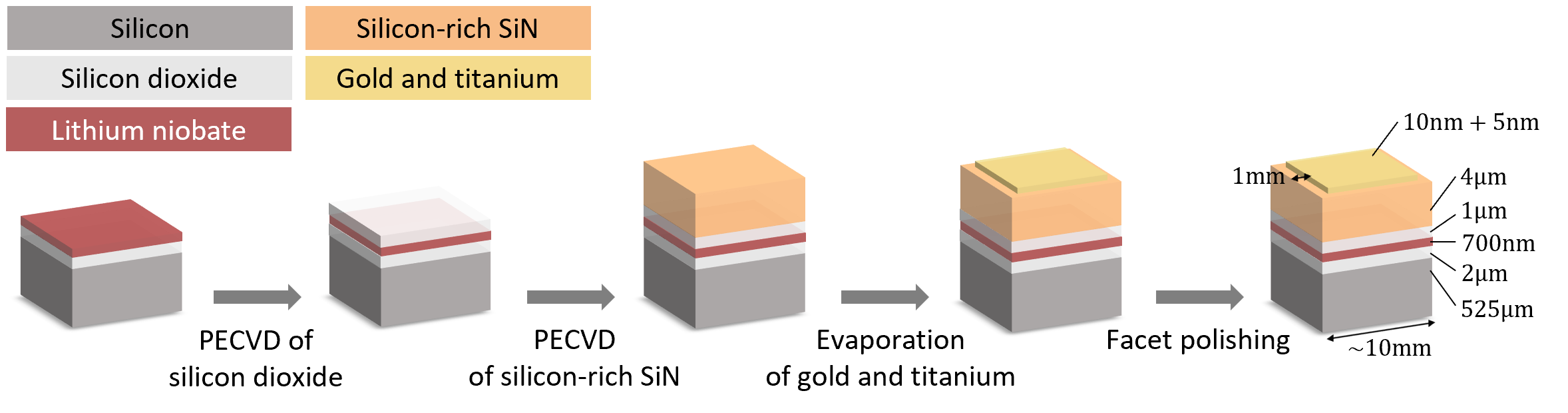
We performed our fabrication processes starting from a thin-film lithium niobate wafer purchased from NanoLN. It is a p-type silicon wafer with a substrate conductivity of 0.01-0.05 , of silicon dioxide deposited via plasma-enhanced chemical vapor deposition (PECVD), and of Z-cut -doped lithium niobate that is wafer bonded with the ion-cut technique. We dice small pieces from the wafer using a Disco Dicing Saw for further processing. We deposited an additional of silicon dioxide via PECVD as a cladding, followed by another deposition of of silicon-rich silicon nitride (SRN), which is the photoconductive layer, via PECVD. The SRN layer was deposited in an Oxford Plasmalab 100 by flowing of , of , and of into the deposition chamber at a temperature of and a pressure of . We alternated pulses of high and low frequency power during deposition to minimize film stress, with , low frequency pulses and , high frequency pulses.
Next, we evaporated electrodes onto the chip using a CVC SC4500 E-gun Evaporation System. We first evaporated of titanium as an adhesion layer, then of gold. To prevent dielectric breakdown between the electrode and the conductive substrate through air at the edges of the chip, we covered the perimeter of the chip with tape during evaporation. The tape acts as a mask, preventing deposition closer than around to the edges, thereby increasing the path length between electrode and substrate through air. To minimize coupling losses into the waveguide, we used an Allied Multiprep Polisher to polish the waveguide facets. We polished using silicon carbide paper of successively finer grain size, starting at , then moving to , and roughness.
A.2 Waveguide design
Choice of core material: We selected lithium niobate as the material for the waveguide core, as it has a large electro-optic coefficient, low optical loss, and thin-film wafers are commercially available. The refractive index change of lithium niobate under an external applied field is given by
| (A.1) |
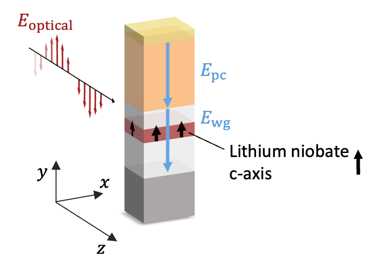
where is the electro-optic tensor, are principal semiaxes of the index ellipsoid, and are the components of the electric field. The strongest component of the electro-optic tensor of lithium niobate is the component. To select the term in the above equation that includes , we need to ensure that the electric field of the optical mode in the waveguide points in the same direction as the externally applied electric field. Since the planar electrode and conductive substrate of our device constrain the applied electric field to predominantly point in the (vertical) -direction, we chose to use a transverse-magnetic (TM) mode such that the electric field of the optical mode also predominantly points in the -direction. Finally, to capitalize on the component, the crystal z-axis also needs to be oriented to point in the -direction in this coordinate system, which is the reason we chose a Z-cut lithium niobate film.
Choice of cladding material: For the claddings of the waveguide, we chose silicon dioxide as it is readily available as buried oxide beneath lithium niobate, and simple to deposit via PECVD as top cladding. It also has desirable material properties for our device, including a high dielectric-breakdown field and low optical loss.
Choice of waveguide dimensions: We designed the thickness of each layer to ensure single-mode waveguiding in the -direction, while maximizing the TM0 mode overlap with the lithium niobate core. At the same time, to optimize the refractive index switching in the lithium niobate core, we minimized the overall thickness of the waveguide (see section A.3) while ensuring minimal substrate loss. These needs were balanced with the availability of thin-film lithium niobate wafers from NanoLN. We settled on a 700 nm thick film of z-cut lithium niobate with 2 µm of silicon dioxide as the bottom cladding and 1 µm of silicon dioxide as the top cladding. This slab waveguide technically has two modes, but the higher order mode has a significant substrate loss ( ), and thus the waveguide is effectively single mode. The cladding thicknesses are chosen to minimize the loss of the mode of the waveguide, which we characterize both numerically and experimentally to be less than (see section B.3 for more detail).
A.3 Photoconductor design
Choice of photoconductor material: We chose silicon-rich silicon nitride as the photoconductor material due to its high dielectric-breakdown field and strong photoconductive response. In addition, the material properties of SRN are easy to tune by varying its silicon-nitrogen ratio [58, 59].
Equivalent circuit model: Here, we explain the electrical modeling of the device. We consider a simplified model, where each small region of the 2D-programmable waveguide is modeled as multiple layers of homogeneous materials with different electrical resistivity for each layer. This simplified model does not address the fringing fields present when a complex pattern of illumination is applied to the photoconductor (a more 3D model is necessary, and is discussed in section B.2), but it is useful for understanding the basic principles of the device. We model each layer as a leaky capacitor, i.e. each layer as a capacitor in parallel with a resistor, and multiple layers are connected in series with each other. The electric field is then a piecewise constant function where the electric field in each material layer is constant and can be found from the corresponding lumped element impedance () via , where and is the layer thickness for layer . The gold electrode and strongly-doped silicon substrate are sufficiently conductive that for the purpose of this analysis they can be modeled as perfect conductors and are ignored in the lumped element model. On the other hand, the lithium niobate core (with cm) and both silicon dioxide claddings are sufficiently electrically insulating that we can model the resistors as open circuits. Therefore, we simplify the circuit for the waveguide, consisting of top cladding, lithium niobate core, and bottom cladding, as a single capacitor with capacitance . Hence, a simplified equivalent circuit to model the device is a single capacitor for the lithium niobate waveguide in series with a leaky capacitor for the photoconductor, where the resistance associated with the leaky capacitor can be reduced via external illumination.
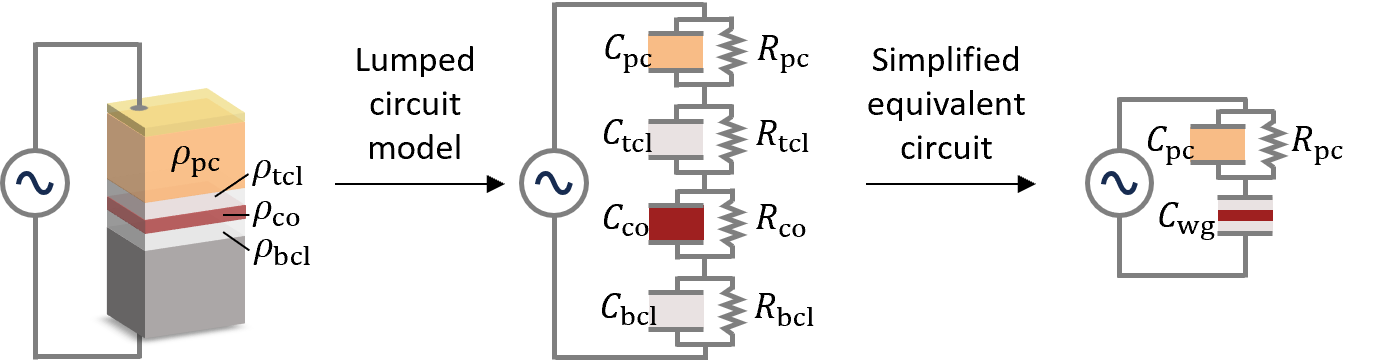
.
Direct current (DC) vs alternating current (AC): Widely used waveguide claddings are extremely good electrical insulators. For example, thermally grown silicon dioxide’s resistivity at room temperature is reported to be more than cm [60]. This resistivity is far higher than the resistivity of silicon-rich silicon nitride and therefore, at DC voltages, the impedance of the device is dominated by the resistance of silicon dioxide. This implies that one cannot change the refractive index of the waveguide with a constant applied voltage, as the steady-state electric field would be zero everywhere except across the silicon dioxide layers and the electro-optic effect in lithium niobate were negligible. We evade this problem by applying AC voltages to our device with frequencies that roughly satisfy . As will be explained in the following section, this will allow us to effectively switch the electric field in the lithium niobate core on and off.
DC operation becomes feasible when waveguide claddings are made of materials with lower resistivity, such as doped silicon oxynitride [61, 62]. Such structures are expected to yield a higher refractive index modulation, due to the reduced impedance of the waveguide. Additionally, they would require a lower operational voltage to achieve the same refractive index modulation (). Consequently, this is a promising direction for future work, which we are actively pursuing.
Choice of photoconductor thickness: In order to design the material stack to effectively switch the electric field inside the lithium niobate core on and off, we optimize the parameters of the circuit and the frequency of the applied voltage. The goal of the design was to find a photoconductor for which the electric field inside the lithium niobate core is as large as possible when the photoconductor is illuminated, and as low as possible when the photoconductor is not illuminated. The photoconductor’s resistance varies depending on the illumination. In the ideal “bright” state (that is, with illumination on the photoconductor), the photoconductor’s resistance is so low that all voltage drops across the waveguide and the electro-optic effect is strongest. In the ideal “dark” state (that is, with no illumination on the photoconductor), the photoconductor’s resistance is so high that the voltage drop across the waveguide is as low as possible and the electro-optic effect is weakest. As mentioned above, it is very challenging to design a photoconductor whose dark resistance is higher than that of silicon dioxide. Therefore, we chose to use AC voltage instead and analyze the complex impedances of the circuit. The voltage drop across the waveguide is given by:
| (A.2) |
Assuming fixed capacitances, this expression is maximal in the limit (“bright” state of photoconductor) and evaluates to , i.e. all voltage drops across the waveguide. The expression is minimal in the limit (“dark” state of photoconductor), and evaluates to . First, this implies that, to maximize the difference of in the bright and dark state, the device needs to be operated with an AC applied voltage whose frequency satisfies . Second, the difference between in the bright and dark state will be larger the larger the ratio . Since the relative permittivities are determined by the choice of materials and the thickness of the waveguide is determined by the considerations presented in section A.2, the only freely tunable parameter is the thickness of the photoconductor . Therefore, a thicker photoconductor layer minimizes the electric field inside the lithium niobate core in the dark state and maximizes the programmable refractive index.
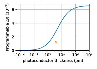
Fig. A4 shows the maximal programmable refractive index as a function of the photoconductor thickness, otherwise assuming the waveguide parameters shown in Fig. A1 and a maximal field of V/µm in the lithium niobate core. The programmable refractive index is defined as the difference between the refractive index in the bright and dark photoconductor state:
| (A.3) |
where the refractive index change in the dark and bright photoconductor state is calculated using Eq. A.1 with the electric field determined from Eq. A.2. For brevity we refer to the programmable refractive index simply as throughout the manuscript. In Fig. A4, the blue line shows the maximal programmable refractive index assuming an optimal photoconductor with and . We selected as thick of photoconductor layer thickness as reasonable ( µm), balancing the benefit from a thicker layer with fabrication constraints (layer stress, deposition time, etc.) and the spatial resolution trade-off discussed in section B.2. The orange cross shows the programmable refractive index that we achieve in experiment, which is lower than the maximal value due to the photoconductor not being perfectly insulating in the dark state and not perfectly conductive in the bright state. More details about this measurement are presented below in Sec. B.1.
Appendix B Device performance
B.1 Magnitude of refractive index change
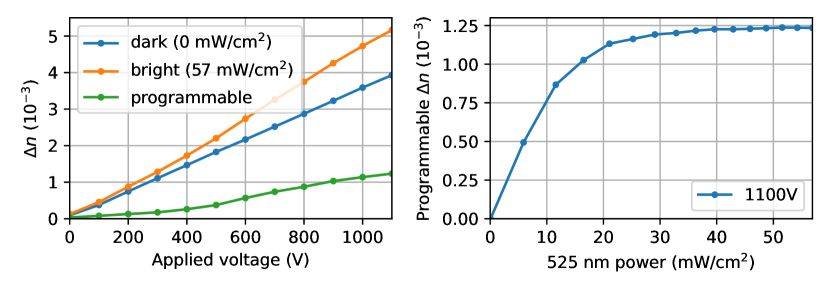
In this subsection, we present measurements of the programmable refractive index as a function of the applied voltage and illumination intensity on the photoconductor. We performed this measurement with an off-axis holography setup, by interfering the light that propagated through the waveguide with an off-axis reference beam (see Fig. A5). All measurements presented here are measurements of the effective index of the TM0 mode, and are given in reference to the refractive index of this mode with no external voltage applied. We measured the refractive index at different applied voltage amplitudes (0 to 1100V) and different illumination strengths (0 - 57 mW/cm2), at a fixed AC voltage frequency of 10 Hz. As shown in Fig. A6A, without any illumination on the photoconductor (“dark”), the refractive index linearly increases with the applied voltage to about at 1100 V. With the photoconductor being illuminated at about 50 mW/cm2, the refractive index change increases to about at the highest voltage of 1100V. We measured the difference between the dark- and bright-state refractive index change, i.e. the programmable refractive index change, to be around at the highest voltage. We also present a measurement of the refractive index change as a function of the illumination intensity, interpolating between the “dark” and “bright” state.
Finally, we note that in Fig. 2 of the main manuscript, the largest achievable is , as opposed to presented here. This discrepancy arises because we conducted the experiments for Fig. 2 at , as opposed to the max voltage applied here of . Moreover, we note that the off-axis holography measurements were performed on a different device than the one used for the main manuscript’s measurements. Variations in the film thickness of the electrode during deposition led to a higher transmission of the illumination through the electrode in the device used for off-axis holography measurements. Thus, more optical power was delivered to the photoconductor, leading to a higher refractive index change.
B.2 Spatial resolution of refractive index change
In this subsection, we discuss an extension to the 1D-model of the electric field inside the waveguide that was introduced in Sec. A.2. The model presented here takes into account the 3D-distribution of electric fields inside the dielectric stack when parts of the photoconductor are illuminated to create a spatially varying refractive index distribution. The considerations in this paragraph show how the spread of the electric field affects the minimal features size achievable in the programmable refractive index distribution.
Inside a dielectric medium with no free charge, the displacement field follows the macroscopic Maxwell equation
| (B.1) |
where is the displacement field at position . Using the constitutive relation , and with the scalar potential , we obtain
| (B.2) |
Here, and are the vacuum and relative permittivities of the medium, respectively. Solving (B.2) under appropriate boundary conditions, we can calculate how the electric field spreads inside dielectric materials.
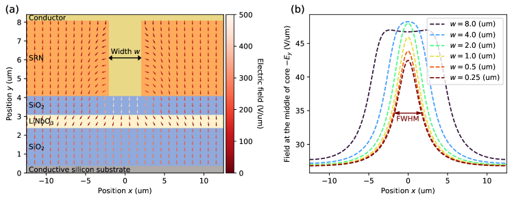
As shown in Fig. A7(a), as a model for the programmable slab waveguide, we consider a stack of layers composed of conductive Si substrate, of bottom cladding, of core, and of top cladding. The layers are stacked in the -direction and are modeled to be infinitely extending in the - and -directions. On top of the top cladding is a photoconductive SRN layer, with a T-shaped conductive region of width in the -direction. The substrate is grounded, and the top conductive region is connected to a voltage source with voltage . We use such a structure to model the situation in which a limited region on the photoconductive SRN is illuminated by a focused light with spot size , making the material locally conductive. It is our goal to use this simplified model to unravel how the spot size is related to the distribution of the electric field inside the core material, studying the impact of electric-field spreading on the spatial resolution we can achieve in light-based programming of refractive index.
For the structures mentioned above, we solve (B.2) using the biconjugate gradient stabilized method. In Fig. A7(a), we show a typical electric field distribution inside the medium for . For more quantitative discussions, we show in Fig. A7(b) the vertical-electric-field distribution at the middle of the lithium niobate core for various conductive strip width . For a large enough , the width of the distribution of is approximately proportional to . On the other hand, as approaches a value comparable to the thickness of the dielectric stacks, the spreading of electric fields sets a finite lower bound to the width of the distribution of . Using the results from , we find the full-width at half maximum (FWHM) of the field distribution to be . This sets a limit to the minimum feature size we can achieve, even in the absence of any diffusion of the carriers inside SRN or finite resolution of the illumination profile impinging onto the SRN.
B.3 Propagation loss
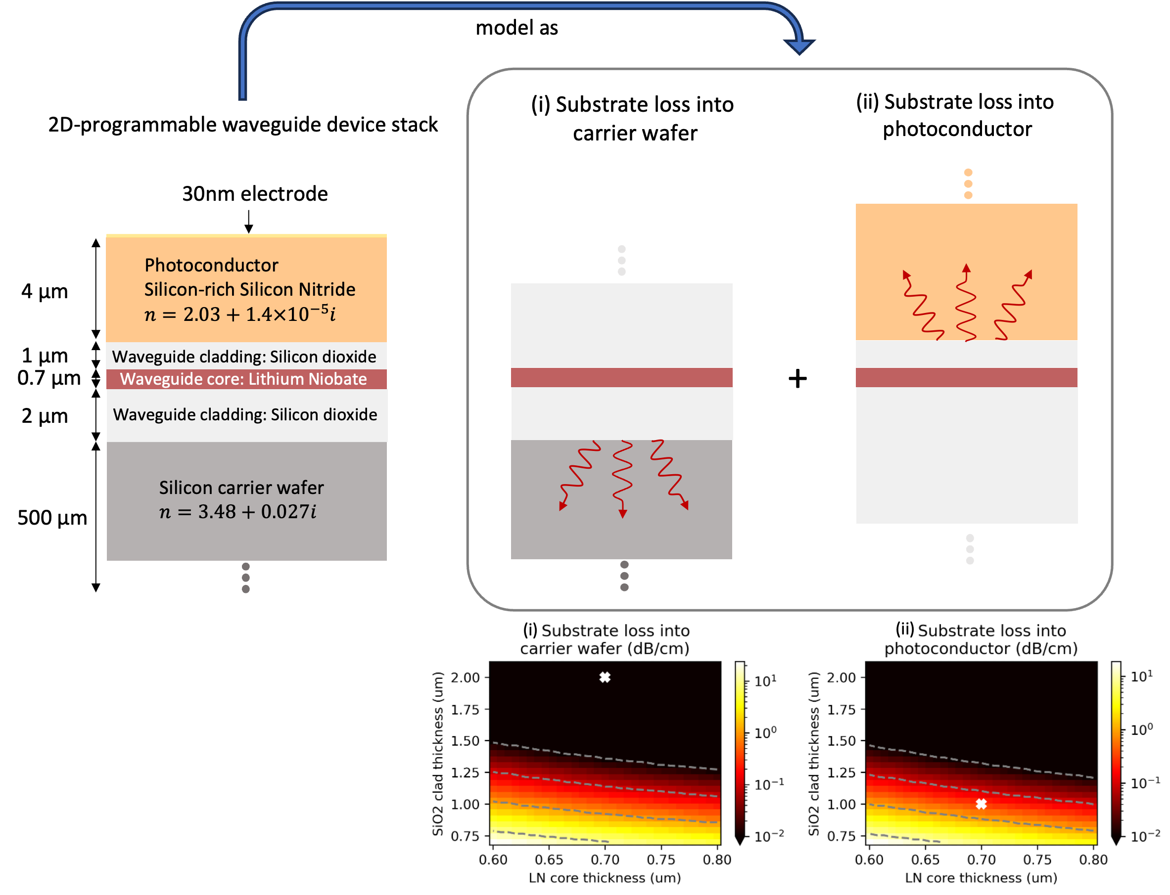
In this section, we discuss the various sources of optical propagation loss in the 2D-programmable waveguide, along with our numerical and experimental characterization of the loss. There are two primary sources of loss in our device: the first is associated with the lithium niobate slab waveguide, and the second is radiative (substrate) loss into the photoconductor and the conductive silicon carrier wafer.
The main source of optical loss in the lithium niobate slab waveguide is attributed to the ion-sliced thin-film lithium niobate wafer from NanoLN, as well as the silicon dioxide deposited via PECVD. According to Ref. [64], the optical loss in the lithium niobate slab waveguide is typically less than for samples that have not been thermally annealed, as is the case with our device. A key factor contributing to the low loss is the absence of lithographic etching in our process, thereby avoiding side-wall induced loss, which is often the predominant source of loss.
The second source of loss in the 2D-programmable waveguide is associated with the photoconductor and the conductive silicon carrier wafer. We measured the material loss of the photoconductor, silicon-rich silicon nitride, to be using a Metricon prism coupler. Thus, the material has a refractive index of . The conductive carrier wafer, a p-type silicon wafer, has a refractive index of . Thus, the loss is primarily due to the optical power of the lithium niobate slab waveguide radiating into the photoconductor and the carrier wafer, rather than being absorbed by the materials. This phenomenon, traditionally referred to as substrate loss, typically pertains only to the carrier wafer. However, given the photoconductor’s substantial thickness (approximately ), it can also be approximately modeled as radiative substrate loss. Therefore, we model this loss in the device as the sum of two independent substrate loss contributions from the silicon carrier wafer and photoconductor (see Fig. A8). The substrate loss is numerically computed using the transfer matrix method [63] for different core and cladding thicknesses. For the carrier wafer, the loss is negligible, below , owing to a thick bottom cladding of . For the photoconductor, the loss is estimated at , attributed to a thinner top cladding of . As loss varies sharply with device parameters, we conservatively estimate that the overall propagation loss in the device loss is below .
Due to the absence of lithographic etching in our device, precise experimental measurement of this numerically estimated low loss is challenging. We fabricated chips of varying lengths (5mm, 1cm, 2cm) and qualitatively observed that transmission through these chips does not vary significantly with length, consistent with the simulations.
Finally, we emphasize that for applications like quantum photonics, the loss can be reduced to be less than by further increasing the top cladding thickness. We also note that it is possible to further enhance device performance, specifically the refractive index modulation (), without a substantial increase in optical loss, by reducing the thickness of the bottom cladding.
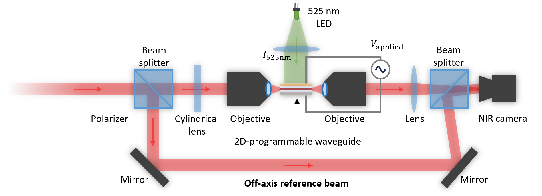
Appendix C Experimental setup
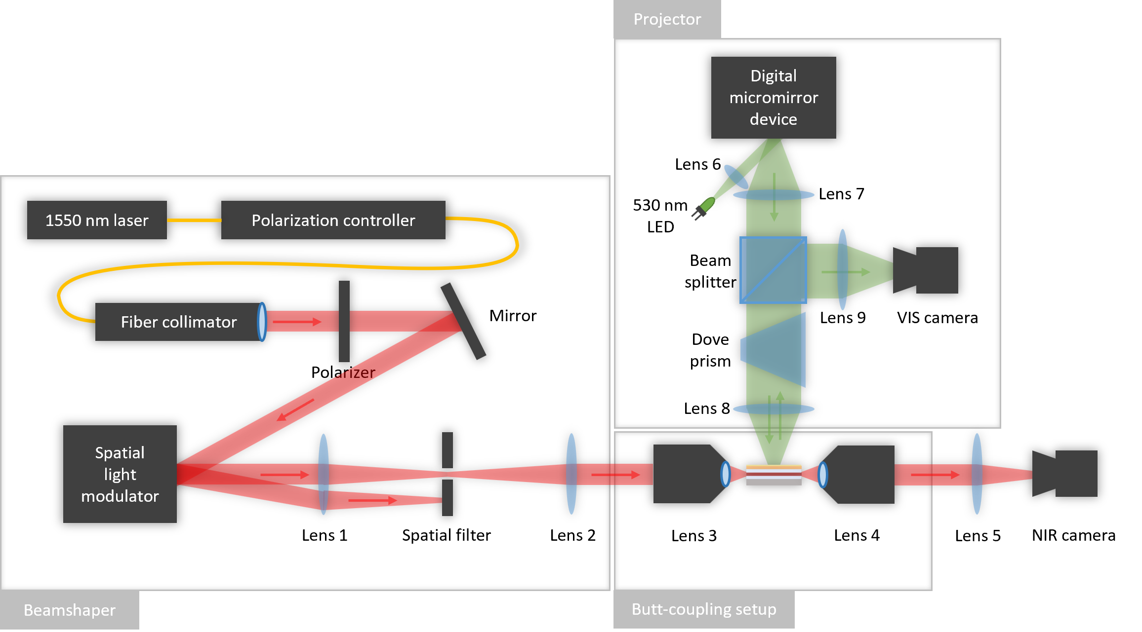
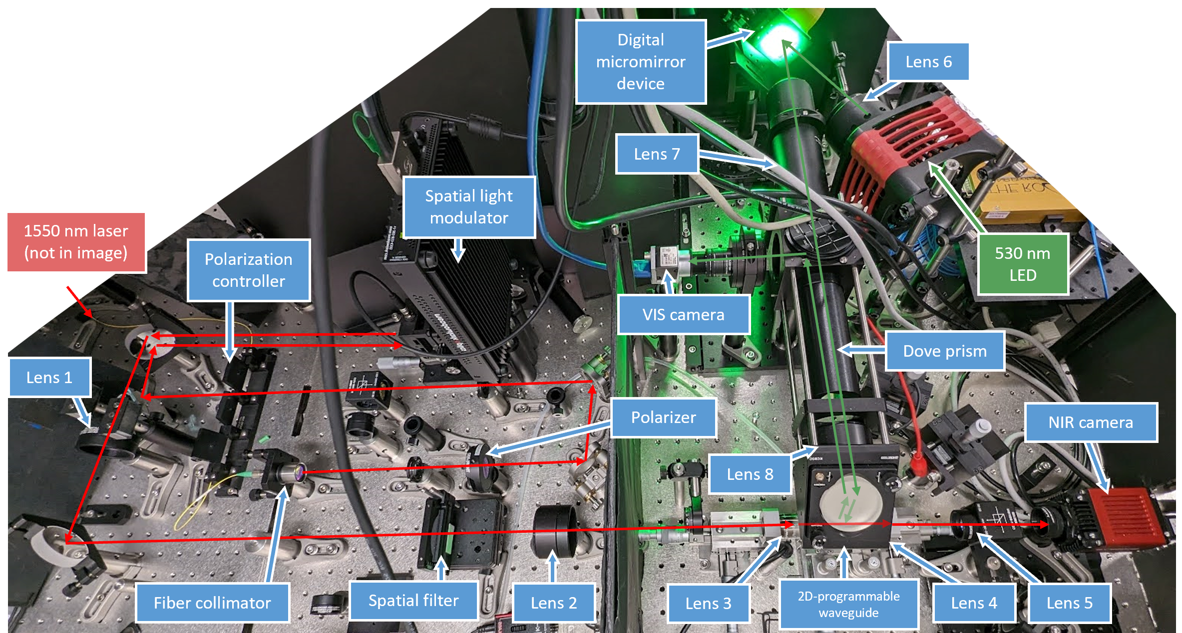
In this section, we explain the experimental setup in detail, which consists of an optical setup and an electrical high voltage setup. The optical setup can be roughly divided into three functional units: 1) A 1D-optical beamshaper to create spatially-varying electric field inputs for the 2D-programmable waveguide, 2) a projector to create a programmable illumination pattern that controls the refractive index distribution inside the waveguide, and 3) a butt-coupling setup to couple light in and out of the 2D-programmable waveguide.
In the descriptions that follow, we reference Fig. A9 and A10 for clarity. To maintain consistency, naming conventions for components within the experimental setup (e.g., “Lens 3”) are aligned with those used in the figures.
1D spatial beamshaper to create optical inputs: The advantage of using a free-space beamshaper lies in its ability to generate arbitrary input electric field distributions. This flexibility enables us to encode high-dimensional input vectors, vary the width of the input modes, and adjust the spacing between them. The design of the beamshaper we built closely follows Ref. [65] that also couples shaped light into slab waveguides.
The core working principle of the beamshaper is to create spatially varying phase-gratings on a 2D-phase spatial light modulator, whose amplitude and relative positions control the amplitude and phase of the 1D optical field at the input facet of the programmable waveguide [66]. We shone a collimated beam of vertically polarized, continuous-wave 1550 nm light from a JDS VIAVI MAP MTLG-B1C10 Tunable DBR Laser onto a Meadowlark Optics UHSP1K-850-1650-PC8 spatial light modulator (SLM). More specifically, the beam from the laser was collimated to a 7mm waist before it hits the two-dimensional phase-SLM, on which spatially varying gratings with a period of 16 pixels are displayed with a pixel pitch of 17 µm. Next, the light propagated through a lens with focal length 500 mm (Lens 1, Thorlabs A1380-C-ML), which separates the diffraction maxima of the phase-gratings displayed on the SLM by approximately 3 mm. A spatial filter (a slit) only lets the first-order diffraction maximum pass through to another lens (Lens 2, Thorlabs TTL200-A, f = 200 mm). From there on, the light propagated to an objective (Lens 3, Olympus UPLFLN 40X Objective, NA = 0.75, f = 4.5 mm) that couples the light into the 2D-programmable waveguide. The second and third lens are essentially a 4F relay system to demagnify the beam at the focal plane of the first lens. Thus, the distribution of light at the input facet of the 2D-programmable waveguide is approximately given by the spatial Fourier transform of the amplitude- and phase-profile corresponding to the gratings displayed on the phase spatial light modulator. We can create arbitrarily input electric fields with features as small as on the input facet, over a distance of . The update speed of optical inputs is approximately 50Hz limited by the response time of the liquid crystal layer of the SLM.
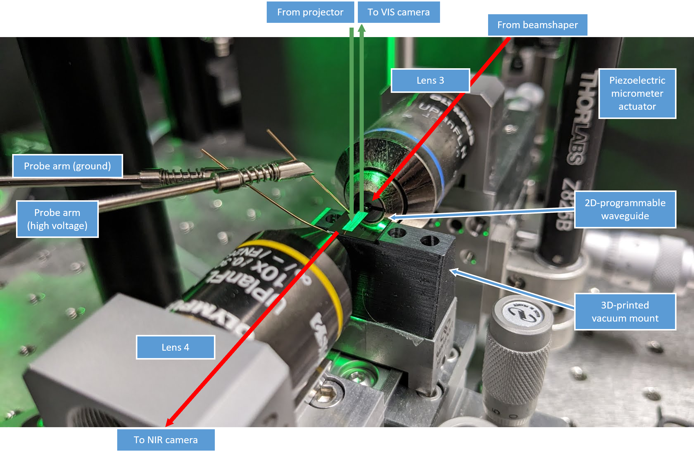
Projector to create a programmable illumination pattern on top of waveguide: To create programmable illumination patterns, we used a digital micromirror device (DMD, Vialux V-7000) with a resolution of 1024x768 pixels and a pixel pitch of 13.7 µm. We illuminated the DMD with green light (525 nm) from a SOLIS-525C high-power LED, collimated by a condenser lens setup (Lens 6). We imaged the surface of the DMD onto the surface of the 2D-programmable waveguide via a 4-f setup consisting of two tube lenses (Lens 7, Thorlabs TL300-A, and lens 8, Thorlabs TTL200-A). To account for the 45-degree rotation of the micromirror array of our DMD, we inserted a Dove prism (Thorlabs PS993M) between the tube lenses, which, appropriately positioned, rotates the image by 45 degrees. Using the same optical path as for the projection, we imaged the surface of the 2D-programmable waveguide onto a camera by inserting an 8:92 (R:T) Pellicle beamsplitter (Thorlabs BP245B1) between the tube lenses and image the waveguide surface via an additional tube lens (Lens 9, TTL100-A) onto a Basler ace acA5472-17um camera. The projection illumination pattern on the surface of the 2D-programmable waveguide has dimensions of , and each individual pixel of the projected pattern is in size.
High voltage setup: In order to maximize the electro-optic effect in lithium niobate, we used high voltages of about 1kV. We created sinusoidal voltages with a Tektronix AFG3102C arbitrary function generator and amplify the voltage with a Trek 2220 high voltage amplifier that has a voltage gain of 200, and can output voltages up to 2kV. We electrically contacted the device using high-voltage-rated probe arms with BeCu probe tips. One probe tip was put in contact with the gold electrode on top of the device, while a grounded probe tip touched the silicon substrate(see Fig. A11).
Appendix D Training the 2D-programmable waveguide to perform machine learning
In this section, we explain how the parameters of the 2D-programmable waveguide is trained to perform machine learning. This includes describing the different training algorithms that we considered, and explaining our decision to use physics-aware training for this work. We begin the section with a discussion on how many parameters are present in our device, as it is a dominant factor that determined the choice of training algorithm.
D.1 Parameter count of 2D-programmable waveguide
The parameters of the 2D-programmable waveguide is the refractive index distribution of the slab waveguide. While it is conceptually advantageous to reason about the refractive index distribution as a continuous function over space, it is in practice a discretized quantity as we use a DMD to project different patterns of illumination on the device, which has a discrete number of pixels. Furthermore, as a single pixel does not exert much phase-shift on the propagation of light, we group pixels on the DMD into macro-pixels for practical implementation. In other words, the number of parameters that we train for the device depends on how finely we perform this discretization, which we outline below.
In the dimension, which is the direction that is perpendicular to the direction of propagation, we chose to use the finest discretization, which is limited by the imaging setup. This is appropriate as finer features in directly lead to more control over the wave dynamics. Thus, the number of independent parameters in the dimension is given by dividing the width of the total area that the wave propagates through () by the smallest pixel size of the projected pattern on the chip ().
For the direction, which aligns with the direction of propagation, the situation differs. To understand this more formally, consider the distance over which a maximal refractive index contrast (the illumination being set to the maximum setting) can induce a phase shift of . This quantity is approximately in our device. Since the length of a single pixel () is much smaller than , each pixel only exerts a negligible amount of phase-shift on the light that is propagating in the direction. Therefore we do not consider each individual pixel to be a freely tunable parameter, but instead only count groups (macropixels) of 11 individual pixels, or , in the -direction to be one tunable parameter. We chose the length of macropixels to be to ensure that each programmed macropixel can induce a non-negligible phase shift of . Thus, the number of independent parameters in the dimension is given by dividing the length of the chip by the length of the macropixel in .
Consequently, the total number of parameters for the 2D-programmable waveguide is given by the product of the number of parameters in each direction, which is approximately in the direction and in the direction, yielding 10,000 parameters.
D.2 Choice of training algorithm
In this subsection, we describe the algorithms we considered for training the 2D-programmable waveguide. There are two critical factors that determined our choice to use physics-aware training: the number of parameters (10,000) for our device, and update speed of our experiment ( for inputs and for parameters).
Model-free training algorithms: These algorithms do not require a digital model to train the physical system. One approach involves individually perturbing each parameter and computing the gradient of the loss function with respect to each parameter [4]. Alternatively, random gradient descent can be used, where the parameters are perturbed in a random direction [9]. Generally, both approaches slow down the rate of training, as a large number of passes through the setup is required to accurately sample the gradient. Given the large number of parameters and the relatively slow update speed of our experiment, this method would have resulted in impractically long training times for the MNIST machine learning task. We note that these algorithms could be effective for training the 2D-programmable waveguide if the number of parameters is reduced, for instance, by a low-dimensional parametrization the projected patterns.
In-silico training: An alternative approach is to use a purely model-based method, termed in-silico training. In this approach, training is performed entirely on a digital computer with the digital model. For differentiable digital models, the physical system can be trained with the backpropagation algorithm, for faster training. After completing the training, the parameters are transferred from the digital computer to the physical system. This requires an excellent digital model of the system. We attempted this approach and found that despite having good digital models (see Sec.E), poor performance was attained on the experiment. For instance, the test accuracy on MNIST is only 60% with in-silico training.
Physics-aware training: In this work, we use physics-aware training, a hybrid in-silico in-situ training algorithm [31]. This method combines the advantages of both model-free and model-based training. Our reasons for choosing this algorithm are as follows. Firstly, it is a backpropagation algorithm. Thus, approximate gradients are computed in a single backward pass, resulting in faster training. Additionally, since the physical system is used to compute the forward pass, the training is able to mitigate the mismatch between the experiment and digital model as well as the effects of experimental noise. A requirement for this approach is a differentiable digital model of the physical system, which we detail in supplementary section E. We will explain physics-aware training in more detail in the following subsection.
In-situ backpropagation algorithms: These algorithms use the physical system to obtain the gradient of the loss function [67, 68, 69]. Thus, a digital model of the system is not required, and the training is fast as the algorithm is gradient-based. However, the algorithm requires having bidirectional input of light [68, 69] and measuring the intensity distribution of light within the chip [65, 70]. For this reason, the method was not implemented in our current experiment. We note that as we scale up the device to a larger number of parameters, this method may become essential for training the 2D-programmable waveguide.
D.3 Physics-Aware Training
This section will explain the physics-aware training algorithm, which is a hybrid in-silico in-situ training algorithm. It is a summary of the algorithm that is specialized for the 2D-programmable waveguide – a more detailed and general explanation of the algorithm can be found in the original paper [31]. The schematic of the algorithm is shown in Fig. A12, which outlines the four key steps of the algorithm. It is also specialized to vowel classification with a single layer, where the input dimension is 12 dimensional and output dimension is 7 dimensional. Finally, we note for brevity that the following equations will assume a batch size of one.
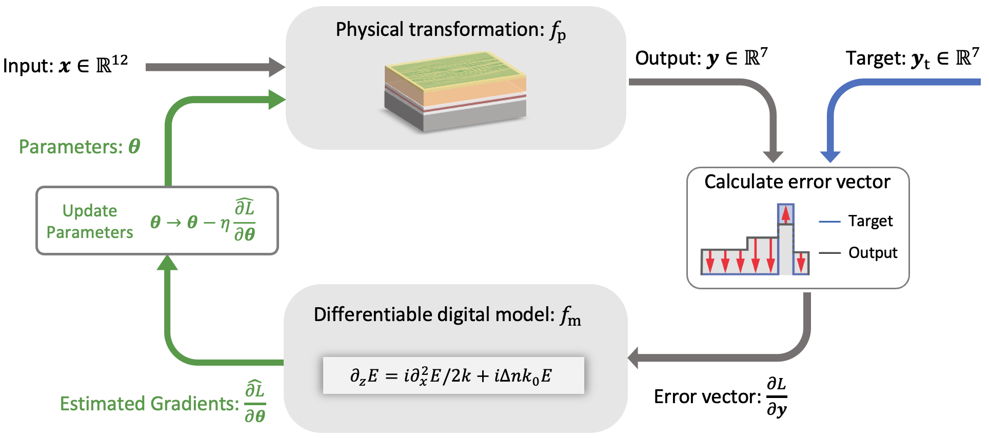
1. Forward-pass through physical system: The first step is to perform a forward pass through the physical system, which in our case is the 2D-programmable waveguide. Mathematically, this is given by
| (D.1) |
Note that the physical transformation includes both the amplitude encoding of the input machine learning data into an input optical field, and the binning operation that converts the output intensity to the machine learning output. Thus, this is a function that takes in an input vector and returns an output .
2. Compute the error vector: Using the output of the physical system and the target output , the second step is to compute the error vector with a digital computer. The error vector indicates how the outputs of the physical system should be adjusted to minimize the loss function, and plays a key role in a backpropagation algorithm. Mathematically, this is given by
| (D.2) |
where the softmax function is used to turn the outputs from the physical system into a probability, and is the cross-entropy function that is usually used as a loss function for classification tasks. One key intuition for why physics-aware training works well is that the error vector is accurately computed, as the algorithm has access to the real output of the physical system.
3. Compute the estimated gradients: The third step is to compute the estimated gradients, which is the approximate gradient of the loss function with respect to the physical parameters. This is done by performing a backward pass through the differential digital model of the physical system . Mathematically, this is given by
| (D.3) |
where is the Jacobian matrix of the digital model of the physical system. The transposed Jacobian matrix performs a matrix-vector multiplication on the error vector to arrive at the estimated gradients. It should be noted that the estimated gradients computed here are approximate rather than exact, as the digital model is only an approximation of the physical system. A key reason for the effectiveness of physics-aware training is that as long as the estimated gradient predicts the direction of the true gradient within a 90-degree cone (), a small parameter update will result in a reduction of the loss.
4. Update the parameters: With the estimated gradients, the final step is to update the parameters of the physical system. This is done by performing a gradient descent step on the parameters. Mathematically, this is given by
| (D.4) |
where is the learning rate. After this, step 1 is repeated, and the algorithm continues to iterate until the loss function converges.
Though the algorithm has been specified mathematically in (D.1)-(D.4), in practice the algorithm is implemented as a custom autograd function in PyTorch. This custom function can be generated via the package Physics-Aware-Training available at https://github.com/mcmahon-lab/Physics-Aware-Training. With the package, the user can run the following line of code to define a custom “physics-aware function”:
f_pat = make_pat_func(f_physical, f_model). The rest of the code can be written in regular PyTorch to train the system. Thus, the user can access regular PyTorch functionality such as optimizers and schedulers for training.
Appendix E Digital model of 2D-programmable waveguide
In this section, we describe the digital model used for the 2D-programmable waveguide. The model is largely physics-based, and is modeled by a partial differential equation. As the calibration and alignment of the chip was complex, we also describe the procedure in this section. Finally, we found that the purely physics-based model only predicts the experimental outputs qualitatively. Thus, to improve the agreement further, we augment the physics-based model with additional parameters, which are trained on experimental data. We outline this data-driven approach to fine-tune the physics-based model in the final subsection.
E.1 Physics-based model
Here, we derive the theoretical model that we use to emulate the 2D-programmable waveguide on a digital computer. To summarize the approach, we begin from the time-independent wave equation (Helmholtz equation) in 2D, and apply the standard beam-propagation method to arrive at the final equation.
The time-independent wave equation in 2D is given by,
| (E.1) |
where refers to the electric field in the dimension as we work with the transverse-magnetic (TM) mode. is the effective refractive index of the slab. We note that the 2D wave equation works well for our setting, as the change in refractive index is generally small [23]. We use the ansatz and apply the slowly-varying amplitude approximation, to arrive at,
| (E.2) |
where is the change in refractive index, which is assumed to be small . in the wavevector in vacuum, is the wavevector in the medium. We note that this equation assumes that the wave is only traveling in the forward direction. This is a good approximation as we did not explicitly train for any resonant structures that could induce significant back reflections. To numerically solve this partial differential equation, we use the split-step Fourier method, which is a numerical method that is commonly used to solve PDEs of this form [71].
Input-output relation: The digital model of the 2D-programmable waveguide is as follows. Recall that the input-output relation is , where and have dimensionalities associated with the machine learning input data and output data. Thus, the initial condition of the field propagation is given by,
| (E.3) |
where are input modes, which we pick to be Gaussian modes whose mean location (in the direction) are translated linearly with respect to the index . By numerically solving (E.2), we can obtain the output field at the output facet of the waveguide . The intensity at the output facet is then binned to arrive at the the machine learning output data , which is given mathematically by,
| (E.4) |
where is the location of the -th bin, and is the width of the bin.
Conversion between projected image and refractive index: As shown in Fig. A6, the relation between the intensity of the projected light on the chip and the refractive index profile is nonlinear as saturation effects set in when the intensity is sufficiently high. However, for machine learning, we have found that operating in the linear regime is beneficial to obtain a better digital model. In addition, the spatial resolution of the refractive index profile is limited due to the spreading of electric-field in the stack, as discussed in Sec.B.2. Taking both of these facts into consideration, the model we use to convert from the parameters, which is the projected image () to the refractive index profile is given by,
| (E.5) |
where is the 2D convolution operation, is a 2D Gaussian kernel with standard deviation , is the maximum refractive index modulation, and is the maximum light intensity of the projected pattern that is illuminated on the chip.
E.2 Initial calibration of physics-based model
Calibration of beamshaper: In this work, we built a beamshaper that enables us to send arbitrarily programmable input field distributions into the 2D-programmable waveguide. As detailed in Appendix Sec. C, the beamshaper is able to set both the amplitude as well as the phase of the input field. Thus, we leverage this capability to calibrate and account for misalignments in the beamshaper. It should be noted that in the future, when an on-chip modulator is used for faster input modulation, this calibration will no longer be necessary.
Mathematically, the miscalibrations of the beamshaper can be characterized as follows:
| (E.6) |
where represents the input field that is set to the beamshaper. , and all represents different kinds of misalignments that will be detailed later. Once these misalignments are characterized, (E.6) can be inverted to accurately send in a desired input field. We use the following procedure to calibrate the beamshaper:
-
•
The coupling efficiency can be characterized by sending in focused Gaussian beam with waist and different mean input location to the input facet of the waveguide, and measuring the overall power at the output facet. We found that the transparency window of coupling efficiency (i.e. drops when is larger than some value) varies as the slab waveguide is rotated relative to the 1D-axis of the input beam. This misalignment can be corrected by rotating the SLM used in the beamshaper. Once corrected, is mostly flat across the entire field-of-view of the beamshaper, which is about 500 wide for our experiment.
-
•
As the beamshaper involves multiple lenses, there are many distances between lenses that could be misaligned. In practice, we observed that the most relevant misalignment is due to the distance between lens 2 and 3 not being equal to +, as this distance changes when a new chip is installed in the setup. When this occurs, the input field picks up a quadratic phase front (), which can be understood as a virtual lens being inserted at the input facet. Thus, this lens imparts a wavevector kick that is a linear function of the input location . To calibrate for this, we send in collimated Gaussian beams () with different mean input location and measure how much the mean output location deviated from the input location. With the formula , can be measured and corrected for.
-
•
To calibrate for , which represents the input beams coming in at an angle instead of being straight, we send in a collimated Gaussian beam () and project two different graded index (GRIN) beamsteerer patterns onto the 2D-programmable waveguide. As shown in Fig. A13, when there is a misalignment, the beam will only be steered by the GRIN beamsteerer in the front, and not the one in the back. By comparing with theory, we can measure and correct for it.
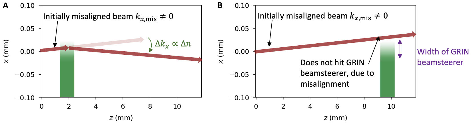
Calibration of programmable 2D-waveguide parameters: Once the beamshaper is calibrated, what remains is to characterize the system parameters of the 2D-programmable waveguide. This is also performed by projecting the GRIN beamsteerers onto the 2D-programmable waveguide.
-
•
The maximal refractive index modulation can be measured by measuring the amount of beamsteering exerted by the GRIN beamsteerer. The change in the -component of the wavevector is linearly proportional to the change in refractive index , and thus can be measured by comparing with theory. We characterized that for vowels classification, while for MNIST classification.
-
•
The spatial resolution of the setup can be measured by varying the width of the GRIN beamsteerer, measuring the amount of beamsteering, and comparing it to theory. Using this procedure, we found that , which is consistent with the theoretical analysis in Appendix Sec. B.2.
In Fig. A14, we show the agreement between the physics-based model and the experimental data for different input fields and different projected patterns on the 2D-programmable waveguide. While the experimental output and predicted output agrees qualitatively in many cases, we observe quantitative differences, especially towards the edges of the output.
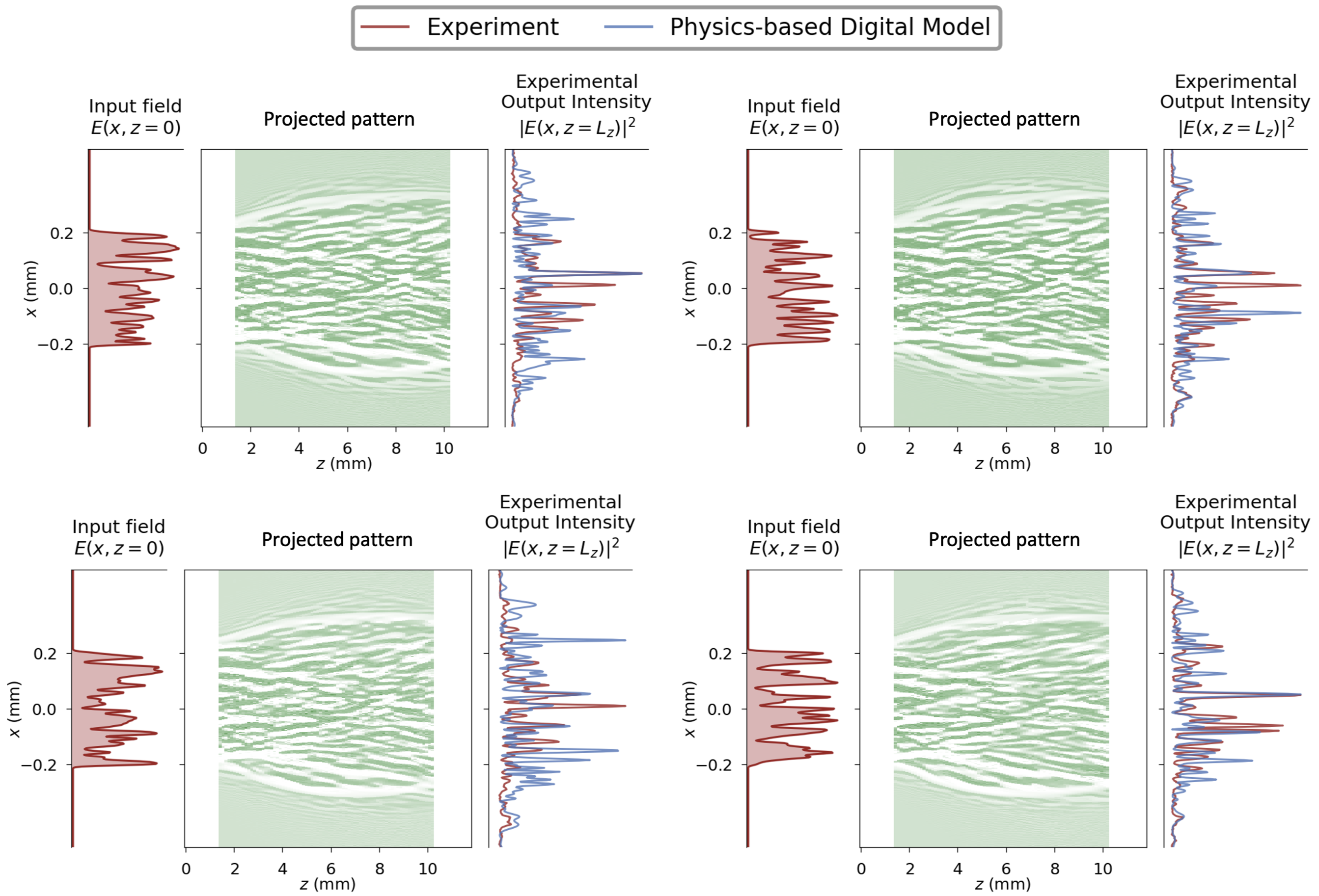
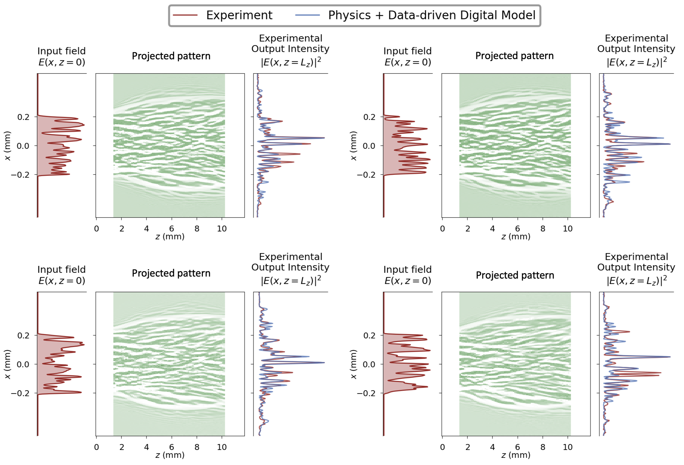
E.3 Data-driven approach to fine-tune the digital model
To further improve the agreement between the physics-based model and the experimental data, we use a data-driven approach to fine-tune the physics-based model. To do so, we add additional trainable parameters into the physics-based model and train them with input-output pairs that are generated from the experimental data.
The model still solves the beam propagation equation (E.2), but now with the refractive index being
| (E.7) |
Here, represents the 2D convolution operation, denotes a background noise refractive index, and is another trainable parameter that quantifies the spatial dependence of induced by a given amount of illumination. The other variables in (E.7) are defined following (E.2). We hypothesize that may be attributed to charge noise in the lithium niobate slab waveguide, previously observed in experiments involving light propagation through lithium niobate, which resulted in effects such as wavefront damage [72]. The parameter accounts for non-uniform illumination in the imaging setup, specifically referring to the spatial variance in power absorbed by the photoconductor across the field-of-view of the 2D-programmable waveguide, even when is intended to be uniform. Additionally, accounts for film thickness variations in the device stack and the potential presence of small domains within lithium niobate where the crystal axis may be flipped [73]. In summary, both and allow the model to address nonidealities associated with lithium niobate, the experimental setup, and the device fabrication.
Finally, we add a trainable output coupling efficiency term to model for potential inhomogeneity in measurement of the output efficiency (). Finally, we also make the previously introduced input coupling efficiency term in (E.6) a trainable parameter.
To collect the training data for the data-driven model, an important detail is to obtain the right distribution of projected patterns that are encountered during machine learning tasks. To do so, we in-silico train the 2D-programmable waveguide in-silico on multiple different variations of the MNIST classification task, with permuted inputs and outputs. This way, we can obtain a large number of distinct projected patterns, which we can then use to train the data-driven model. For the input fields, we send in input field distributions with random amplitude and phase in a pixel mode basis. In other words, they are generated with (E.3) with being random in both amplitude and phase. Using many experimentally measured input-output pairs, we train all of these additional parameters (, , , ) on a digital computer with the backpropagation algorithm.
In Fig. A15, we show the agreement between the experimental data and revised digital model that is augmented with a data-driven approach. We see that the agreement has improved significantly compared to the physics-based model, especially at the edges of the output (at large ).
Appendix F Machine learning
In this section, we present additional information regarding the machine learning tasks that we performed on the 2D-programmable waveguide.
F.1 Computational Model of ONN demonstrations
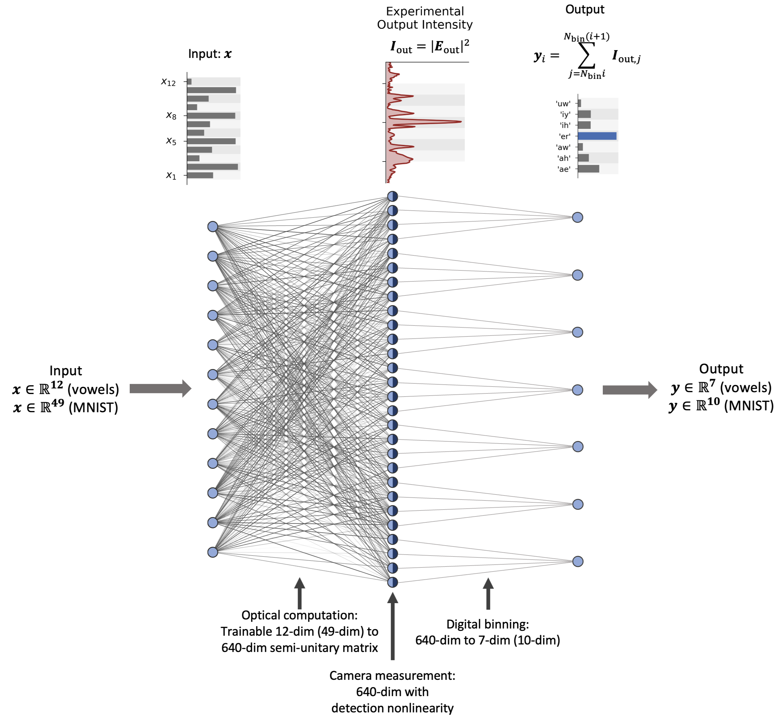
In this section, we explain the computational model of the optical neural network demonstrations performed by the 2D-programmable waveguide. For concreteness, we focus on the vowel classification task, which has a 12-dimensional input and 7-dimensional output, and the MNIST classification task, which has a 49-dimensional input and 10-dimensional output. At the end of the section, we argue that the computation performed by the 2D-programmable waveguide is similar to that of a 1-layer neural network, and we use this to characterize the computational complexity of the device.
The input vector is encoded in the amplitudes of 12 (49 for the MNIST task) spatial Gaussian modes via (E.3). Since each Gaussian mode is normalized, this can be abstracted as a unitary relation: , where represents the input field in a pixel basis. The propagation through the device is also a unitary operation, it that takes the input field and returns the output field . Thus, the output field is given by . In this notation, we see that by training the refractive index distribution, we are able to change the unitary matrix applied by the device . Moreover, since the first two operations can be collapsed into a single unitary matrix, the device’s overall operation can be expressed as , where . Here, ( for MNIST), as we discretize the output field into a 640-dimensional vector defined by the number of pixels on the camera used to measure the output.
We model the measurement of the intensity at the output facet by a quadratic nonlinearity applied to the optical field: . After the camera measurement, we digitally bin groups of camera pixels – average pooling in machine learning language – to create a lower-dimensional output of 7 (10 for MNIST). In summary, the computation performed can be expressed as
| (F.1) |
where the matrix vector multiplication is performed optically, the nonlinear activation function is performed by the analog electronics of the camera, and the fixed average pooling is performed by a digital computer. This relation is also shown schematically in Fig. A16. We note that the entire computation could be performed without a digital computer, for example, by using a lens to optically perform the fan-in operation, and using a photodetector for each class of the classification task.
We emphasize that although we can train the unitary matrix by programming the refractive index distribution, it is not possible to realize an arbitrary . This limitation is physically intuitive as the number of parameters in (125440 for the MNIST task) exceeds the number of parameters available in the 2D-programmable waveguide (10,000).
While the input-output relation defined in (F.1) is mathematically equivalent to a 2-layer neural network, the computation it performs is similar to that of a 1-layer neural network due to the second layer being sparse and not trainable, and the square nonlinearity not being significantly nonlinear (compared to activation functions such as ReLu and Sigmoid). An alternative argument is that if the square nonlinearity were replaced with an identity operation, (F.1) would indeed reduce to a 1-layer neural network. Therefore, we characterize the complexity of the computational operation performed by the 2D-programmable waveguide by the number of operations performed by the effective 1-layer neural network, rather than the number of operations in .
The most complex machine learning task we have undertaken with the 2D-programmable waveguide is the MNIST task, where it achieves an 86% accuracy, moderately close to the 90% accuracy achievable by a 1-layer digital neural network (with 49 inputs and 10 outputs). Hence, we characterize the device as capable of performing 490 multiply-accumulate operations in a single pass through the chip.
F.2 Vowel classification
Experiment Settings: The frequency of the AC voltage drive is set to , to increase the speed of data collection. The amplitude of the AC voltage was set to instead of (as in Fig. 2 of the main manuscript), because this experiment was performed at an earlier stage of the project, when we used a more conservative voltage buffer for the device. These two choices led to a decrease in the maximal refractive index modulation to , compared to shown in Fig. 2 of the main manuscript.
Additional Results: In Fig. A17, we show how the wave propagation evolves during the training process. The 4 projected patterns shown on the left corresponds to the same projected patterns shown in Fig. 3 of the main manuscript. The same input vector is also used for consistency, whose correct label is the vowel ‘er’, which corresponds to the 4-th bin in the output. We observe that at initialization, the projected pattern is uniform, and the output intensity is unstructured uniformly spread across all of the 7 bins. After just 1 epoch of training, the wave propagation is already significantly altered, where there is much more structure in the output.
We emphasize that small changes (to the visual eye) in the projected pattern can lead to large changes in the wave propagation. This is particularly evident in the case of the last two projected patterns, at Epoch 20 and Epoch 300. Although these patterns appear similar, the wave propagation differs significantly. More power is concentrated in the bin that corresponds to the correct vowel by Epoch 300. This highlights the importance of an in-situ programmable device for controlling complex wave propagation.
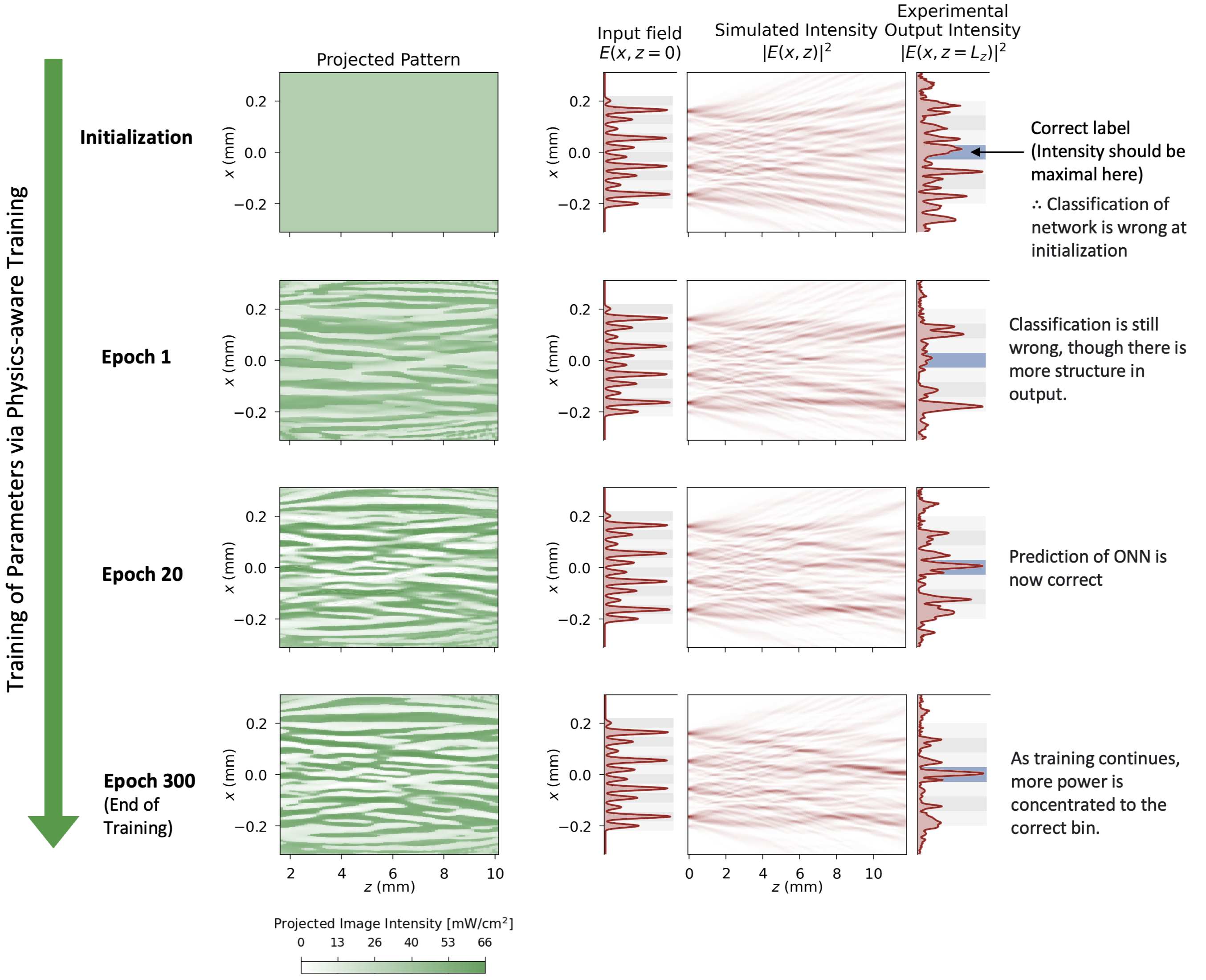
F.3 MNIST classification
Experiment Settings: The frequency of the AC voltage drive is set to , to increase the speed of data collection. The amplitude of the AC voltage was set to , consistent with Fig. 2 of the main manuscript. Therefore, there is slight decrease in the maximal refractive index modulation to , compared to shown in Fig. 2 of the main manuscript.
For the MNIST experiments, the maximal refractive index modulation is . This is because we increased the frequency of the AC drive from to , to increase the speed of data collection. We operated the device at , therefore the maximum change in refractive index is larger than that of the vowel classification experiments.
Additional Results: In Fig. A18, we show additional results regarding the MNIST classification task. Fig. A18A shows the parameters of 2D-programmable waveguide, the projected pattern, after training. When compared to the projected patterns for the vowel classification, we observe that more the of the patterns takes on more extreme values, where many pixels are at maximum or minimal intensity. This suggest that the MNIST task is more difficult than the vowel classification task, pushing the capabilities of the device closer to its limit.
In Fig. A18B, we show the wave propagation for the particular input MNIST image shown in Fig.4 of the main manuscript. The wave propagation is more complex than that in the vowel task. We note that we chose the width of the Gaussian input modes (used to generate the input field) to be , to limit the diffraction of the modes, while the spacing between the modes is . Thus, the input modes used in (E.3) overlap, resulting in the input field shown in Fig. A18B. This is not a fundamental limitation and will be addressed in future work.
Finally, in Fig. A18C, we present the training curve for the MNIST classification task. We observe fluctuations in accuracy; for instance, at epoch 8, it reached 87.2%. The accuracy is 86.2% after 10 epochs of training, compared to the 90% accuracy achieved by a 1-layer digital neural network on the same 49-dimensional MNIST task.
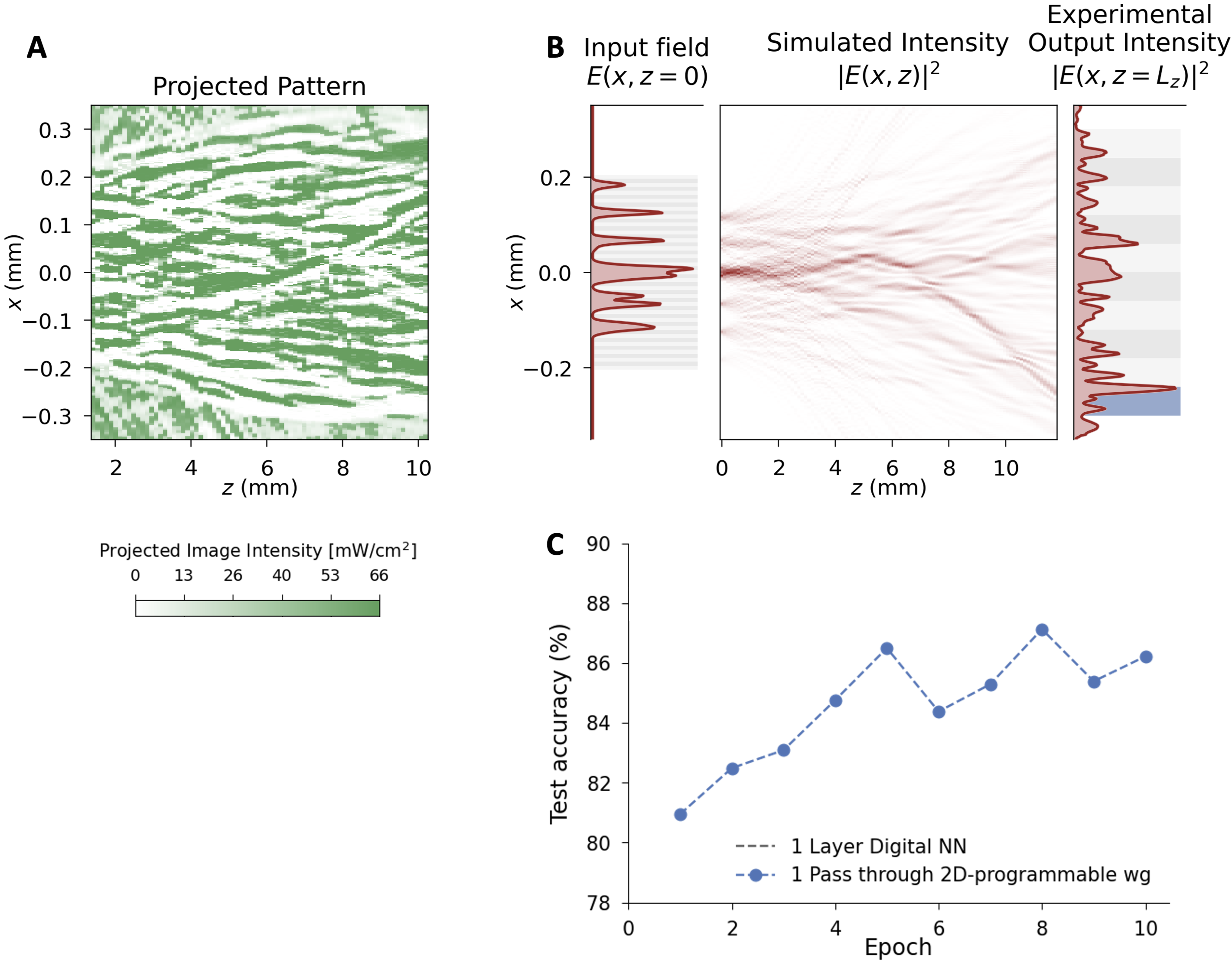
Appendix G Comparison with other on-chip optical neural network demonstrations
In this section, we compare our work with other on-chip optical neural network demonstrations §§§We have not included references, such as Ref. [74], if they don’t report machine-learning-inference accuracy., focusing particularly on demonstrations that perform matrix-vector multiplication (MVM) with a weight-stationary approach, where the matrix elements are encoded in programmable elements on the chip.
We acknowledge that various metrics can be used to compare the performance of different on-chip optical neural network demonstrations. Here, we focus on the number of multiply-accumulate operations (MACs) executed in a single pass through the device. For a single-layer neural networks, the number of MAC operations is determined by the product of the input and output dimensions of the MVM operation. In multi-layer neural networks, it is the sum of each layer’s MAC operations. For ONNs utilizing frequency multiplexing, the number of MAC operations is multiplied by the number of channels, , used for frequency division multiplexing. Additionally, we also compare the devices’ compactness, measured by the number of MAC operations per unit area. Here, “area” specifically refers to the portion of the chip where light propagates to perform the MVM and excludes regions dedicated to electrical wiring and bond pads.
| Reference | MVM Scheme | MACs | Area [] | Compactness [MACs/] | ||||
| This work | Multimode wave propagation | 1 | 1 | 49 | 10 | 490 | 12 | 41 |
| [4] | Mach-Zehnder mesh | 1 | 1 | 4 | 4 | 16 | 0.8 | 20 |
| [9] | Mach-Zehnder interferometer | 3 | 1 | 6 | 6 | 108 | 5.3 | 20 |
| [12] | Photonic-electronic neuron | 3 | 1 | 30 | 2 | 66 | 2.3 | 29 |
| [10] | Photonic tensor core with PCM memory | 1 | 4 | 4 | 4 | 64 | 3 | 21 |
| [38] | Microring resonator weightbank | 1 | 4 | 1 | 4 | 0.2 | 20 | |
| [24] | Imaginary-index-driven arbitrary matrix processor | 1 | 1 | 8 | 4 | 32 | 0.17 | 188 |
The table demonstrates that the 2D-programmable waveguide has demonstrated the largest input and output dimensions, as well as the highest number of MAC operations among the on-chip optical neural network demonstrations reviewed. In terms of compactness, the 2D-programmable waveguide is also highly competitive, ranking second only to the imaginary-index-driven arbitrary matrix processor [24]. As discussed in the main manuscript, this work shares many parallels with ours, notably in its avoidance of discrete programmable photonic elements and in leveraging a continuous, spatially programmable slab waveguide (in their case a spatial gain/loss distribution) to perform neural-network computations.
Appendix H Future device improvements to the 2D-programmable waveguide
††footnotetext: Multilayer ONNs have been demonstrated in a related work [11] on this platform.H.1 Potential routes to a fully integrated 2D-programmable waveguide
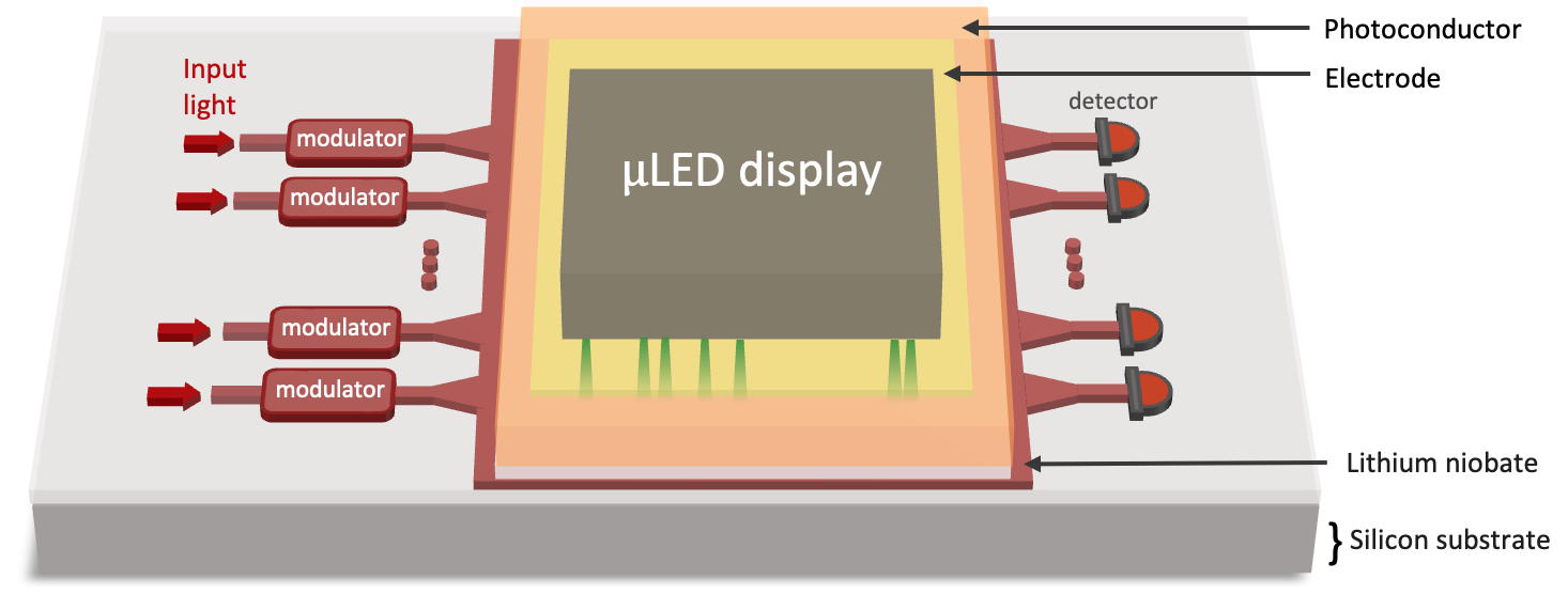
In this section, we discuss potential routes to a fully integrated 2D-programmable waveguide that would be more compact. The components currently occupying the most space in the current setup are the beamshaper, the detection setup, and the projector, thus we address how to integrate these components on-chip.
Fig. A19 shows a conceptual schematic of a fully integrated 2D-programmable waveguide that could be built in the future. Input fields can be created with an array of on-chip lithium niobate modulators. Due to the strong electro-optic effect in lithium niobate, these modulators have been shown to have high bandwidth at low operating voltages [41]. These inputs can be directed into a region of the chip featuring the programmable refractive index distribution. It is important to fan out the waveguide mode to a larger width before entering this region, as the programmable 2D-waveguide region can only control beams with a finite spatial bandwidth , due to the low numerical aperture associated with the maximum refractive index contrast in the 2D-programmable waveguide. The detection setup can be replaced with an array of on-chip photodetectors. Although integrating photodetectors on lithium niobate is generally challenging, there has been progress, including heterogeneously integrated III-V materials [75], as well as the integration of 2D-material [76], and tellurium thin films [76, 42]. High bandwidths of over 40GHz have been demonstrated with these approaches [42]. For both the modulator and the detector, it is crucial to add the capability to lithographically etch the lithium niobate layer in the 2D-programmable waveguide. This should be feasible by depositing the photoconductive layers (via PECVD) onto a designated region, separate from the region where the lithium niobate is etched for modulators and detectors.
In our current experiment, we use a DMD, illuminated by a green LED to project a programmable illumination pattern onto the 2D-programmable waveguide. As shown in Fig. A19, this programmable illumination can be projected in a more compact manner by bonding a micro-LED display (µ-LED) directly onto the electrode of the 2D-programmable waveguide. Among the different display technologies, which includes LCDs, organic LEDs (OLEDs), and micro-LEDs, micro-LEDs are the most promising, because they offer high brightness and small pixel pitches. In fact, displays with 30,000 PPI and a brightness of 100,000 nits have been demonstrated [77]. This corresponds to a pixel pitch of 0.87 , and assuming that 50% of the light emitted is absorbed by the photoconductor, this corresponds to an optical intensity of . Thus, such micro-LEDs can deliver sufficient optical power to the photoconductor, for the operation of the 2D-programmable waveguide (see Fig. A6). The key technical challenge will be in getting the LEDs close enough to the waveguide to ensure that the emitted light does not diffract significantly before it is absorbed by the photoconductor. In order to do so, the protective layer (encapsulation) over the LEDs will first need to be either removed or partially etched down to a thin layer. Alternatively, micro-LEDs with monolithically integrated micro-lenses can be used [78].
H.2 Simulations of unitary matrix operations with a prospective, scaled-up 2D-programmable waveguide
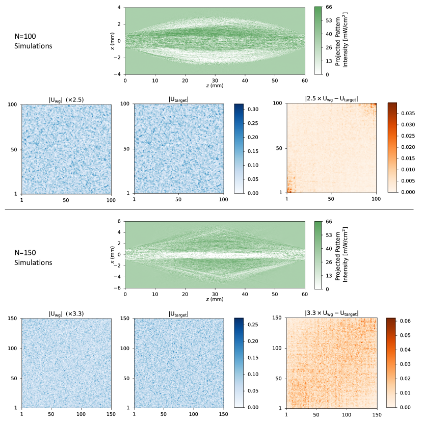
In this section, we present simulations of performing large-scale unitary matrix operations with a 2D-programmable waveguide that has a length of and a maximal refractive index modulation of . Both of these parameters are five times larger than those of our current experiment ( and ).
In order to perform unitary operations, we decompose the output field in discrete output modes. Thus, we do not use the output encoding used in the experiments, where we measure and bin the output intensity distribution, but instead assume that there are output waveguides that filter the output field into discrete modes (this is also the output encoding shown in Fig. A19). We perform simulations for input and output vectors of dimensions and , for random unitaries sampled from the Haar measure. The input and output modes are assumed to be the same. For , the width of the Gaussian modes (“radius” at which the field amplitudes fall to ) is , while the spacing is (thus the inputs span a distance of ). For , the width of the Gaussian modes is , while the spacing is (thus the inputs span a distance of ). We note that the matrix operations are performed up to a rescaling factor, which represents loss. The was performed with a transmission of 16% (loss of 84%), while the was performed with a transmission of 9% (loss of 91%). Adding this rescaling factor to the training eases the burden on the programmable wave propagation, as it no longer has to funnel all of the powers into the discrete and incomplete basis of output modes.
The results are shown in Fig. A20. We observe that the 2D-programmable waveguide is able to execute the unitary matrix operations with high fidelity for the case. For , the fidelity is lower, but the matrix elements of the target unitary matrix and the matrix performed by the 2D-programmable waveguide still agree to within 25%.