Anomalous acousto-current within the quantum Hall plateaus
Abstract
We systematically study the acousto-current of two-dimensional electron systems in the integer and fractional quantum Hall regimes using surface acoustic waves. We are able to separate the co-existing acoustic scattering and drag, when phonons induce drag current and tune the electron conductivity, respectively. At large acoustic power, the drag current is finite when the system is compressible and exhibits minima when incompressible quantum Hall effects appear. Surprisingly, it exhibits anomalously large bipolar spikes within the quantum Hall plateaus while it vanishes linearly with reduced acoustic power at compressible phases. The current peaks reverse their polarity at the two flanks of exact integer or fractional fillings, consistent with the opposite electric charge of the quasiparticle/quasihole.
Ultra-high mobility two-dimensional electron systems (2DES) exhibit quantum Hall effect[1] when subjected in high perpendicular magnetic field . An incompressible superfluid phase that can host dissipationless current at extremely low temperature [2, 3, 4]. Their quasiparticle excitations are anyons with topological phases and have attracted tremendous interests, especially those of the 5/2 fractional quantum Hall state who might obey non-Abelian statistics and be useful for topological quantum computing [5, 6]. Varies experimental techniques are employed to study the quasi-particles’s properties, including weak tunneling[7, 8, 9, 10], interferometry[11, 12, 13, 14], shot noise[15, 16, 17, 18] and thermal transport[19, 20, 21], etc.
Surface acoustic wave (SAW) is a useful technique which studies 2DES through the electron-phonon interaction [22, 23, 24, 25, 26, 27, 28]. It is a special acoustic wave that propagates along the interface between materials with different acoustic velocity. In piezoelectric materials such as GaAs, SAW can be launched by applying an excitation voltage to the emitter interdigital transducer (IDT) and detected by measuring the induced voltage on the receiver IDT [29]. In these materials, the electron-phonon interactions are enhanced by the piezoelectric field accompanying the mechanical vibration. Studying quantum phenomena in 2DES through the acoustic propagation properties, i.e. its attenuation and velocity shift, is a heavily exploited technique [30, 31, 32, 33, 34, 35, 36]. The electron-phonon interaction can also transfer momentum from propagating phonon to electrons and induce a current. Pioneering studies have observed the flow of such phonon drag currents (or equivalently the accumulation of longitudinal voltages) under various experimental conditions [37, 38, 39, 40, 41, 42, 43, 44, 45, 46, 47, 48].
In this study, we conducted a systematic and thorough investigation of the acousto-current in both the integer and fractional quantum Hall regime. After carefully optimizing the measurement, we are able to separate two co-existing phenomena: the phonon-drag effect that describes the current driven by acoustic waves and the phonon-scattering effect when the 2DES conductivity is tuned by the acoustic waves. When the input acoustic power is orders of magnitude lower than previous studies, we discover an anomalously large phonon drag current within the conduction plateaus at quantum Hall effects surprisingly. This phenomenon exists even at the fragile 5/2 quantum Hall effects.
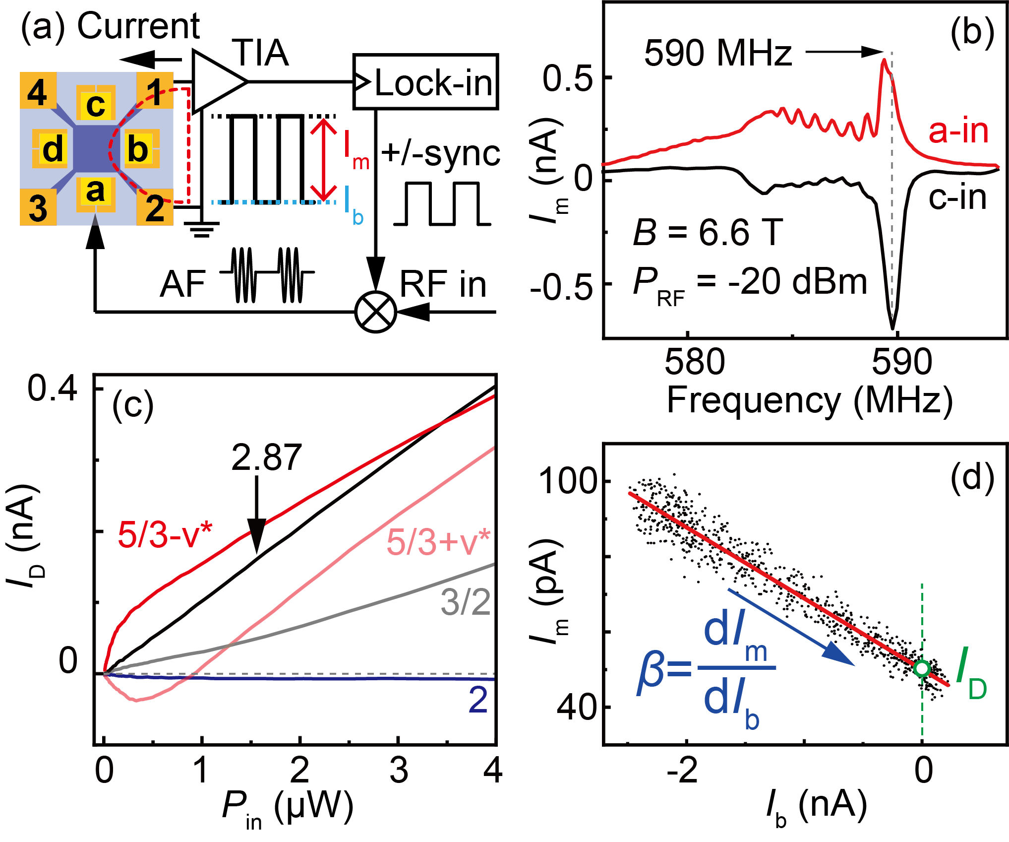
In this work, we investigate an ultra-high mobility 2DES confined in 30-nm-wide GaAs quantum well whose density is and low temperature mobility is . The 2DES mesa (dark blue region in Fig. 1(a)) has a Van der Pauw geometry with four evaporated Au/Ge/Ni/Au contacts (gold square labeled 1 to 4). Two pairs of 5-m-period IDTs evaporated on each side (gold square labeled a to d) converts the input voltage into SAW propagating along the crystal direction111 All doping layers underneath the IDTs are removed by wet etching to avoid unwanted signal coupling. The typical attenuation of our delay-line device is approximately - 30 dB.. We parameterize the acoustic power by the input microwave power . The typical attenuation of our delay-line device is approximately - 30 dB[50]. The current is measured by a compact, battery powered trans-impedance amplifier (TIA) with carefully designed current loop to achieve leak current [51]. A lock-in scheme is used to measure the acousto-current from the TIA output voltage; see Fig. 1(a) and its caption. The measurements are carried out in a dilution refrigerator whose base temperature is below 20 mK.
The SAW consists a continuous flow of monochromatic phonons and interacts with 2DES by exchanging momentum and energy via electron-phonon interaction. At - 20 dBm, the process of transferring momentum from phonons to electrons, i.e. phonon drag, dominates. Fig. 1b shows that the measured acousto-current has a peak at about 590 MHz when the excitation frequency is close to the IDT resonance frequencies ( is the spatial period of the IDT and is the SAW velocity). The dragged electrons move along the same direction with the phonons (which is from IDT a to c), so that a positive current flows into the sample from contact 1. The current changes its polarity if we reverse the phonon direction by exciting IDT c instead of a; see Fig. 1(b). Furthermore, the drag current is proportional to , see Fig. 1c. All these observations agree with previous reports where up to A drag currents is obtained using dBm [37, 46, 45].
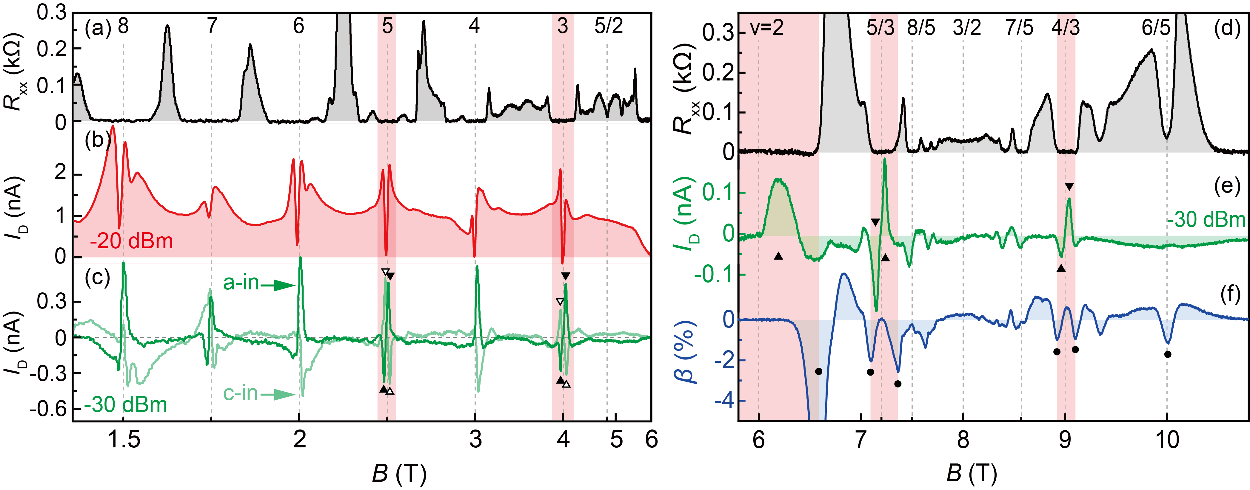
In Fig. 2(a), the longitudinal resistance exhibits zero plateaus at integer quantum Hall effect, as well as clear minima corresponding to fractional quantum Hall effects at Landau level filling factor , 7/3, etc. Fig. 2(b) shows the drag current measured at - 20 dBm. has minima at integer , consistent with the incompressibility of quantum Hall liquid. The minima at integer in Fig. 2(b) are considerably narrower than the plateaus (highlighted by the red shading), while previous studies suggest that should be similar with [52, 38, 43]. This is possibly related to the fact that the electrons’ mean free path in our ultra-high mobility samples ( m) is much larger than the 5 m acoustic wavelength. A rigorous theoretical treatment is necessary.
The - 20 dBm used in Fig. 2(b) is comparable with, if not much lower than, any previous studies. The drag current nA is much smaller than typical current used in transport measurements. Note that nA means that SAW carries electrons per cycle. The vs. is roughly linear in Fig. 1(c) at most fillings. The fact that is always positive evidences that the particles being dragged by SAW always have negative charge. The estimated induced charge density is approximately cm-2 (see the supplementary material of Ref. [50]), much smaller than the thermal fluctuation k cm-2 at 10 mK. However, even such a small excitation might already be too large for studying fragile phases.
The vs. relation near exact integer or fractional filling becomes nonlinear when we reduce the excitation power to below 1 W (-30 dBm); see Fig. 1(c). Note that pA corresponds to less than 1 electrons per each acoustic period moving from contact 2 to contact 1! The measured in Fig. 2(c) becomes dramatically different from the Fig. 2(b) data. decreases to nearly zero when the 2DES is compressible, agreeing with the linear vs. dependence in Fig. 1(c). Surprisingly, in contrast to the minima seen at integer in Fig. 2(b), we observe large current peaks in Fig. 2(c) within the plateaus (highlighted by the red shading). The polarity of the current peak reverses when we switch the SAW direction, confirming the phonon-drag-origin of these peaks.
It is quite interesting that these current peaks have a bipolar feature, namely at exact integer and it has a pair of positive and negative peaks at slightly non-integer . This feature suggests that they are related to the momentum transfer from phonons to the quasiparticles/quasiholes, which appear at slightly larger/smaller (lower/higher ) and have negative/positive electric charge. This bipolar feature is clear at odd fillings , 5, etc., and the high-filling-side peaks at even fillings , 4, 6, etc. disappear [51]. This is likely related to the fact that the Fermi level at odd fillings resides between Landau levels separated by the small spin splitting , while it jumps between Landau levels separated by at even fillings. The large Fermi energy discontinuity at even integer leads to stronger confining potential for localized quasiparticles.
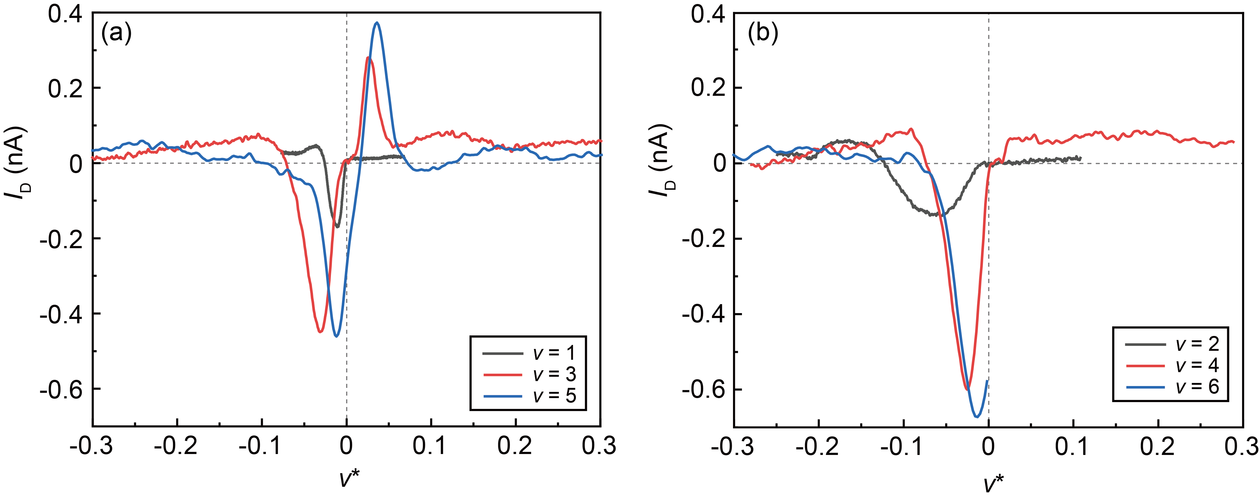
This bipolar current peaks also appear at fractional quantum Hall effects. Fig. 2(e) shows measured at - 30 dBm and . is less than 10 pA when electrons form compressible composite Fermion Fermi sea at . Large and clear bipolar current peaks appear within the plateaus at the and 5/3 fractional quantum Hall effect. If we further reduce to - 40 dBm, the bipolar current peaks becomes visible at and 6/5, see Fig. 3(a).
A schematical model was proposed to describe the origin of the drag current by electron-phonon interaction [38, 53]. The phonons interact with 2DES through the piezoelectric field which is screened by the induced spacial electron density fluctuation . The conductivity has a dependence on the local particle density, i.e. , which leads to a correction to the local current density . The time averaging of this correction term contributes a DC current proportional to . It is quite suggestive to observe a similarity between and in the fractional quantum Hall regime at T, since the SAW velocity shift depends on [51]. However, the fact that large and sharp peaks appear only within strong quantum Hall plateaus, suggests that the presence of Wigner crystal and superfluid quantum Hall liquid is important. A microscopic model describing the dynamics of these quantum phases would be necessary to understand our observations.
The phonons not only induce a drag current by transferring momentum to the electrons, it also changes the sheet conductivity by scattering moving electrons. The latter mechanism induces a scattering current when a DC current flows through the sample. Both the drag and scattering current are induced by phonons, and will be part of the measured signal . The scattering current is naturally proportional to the DC bias current and is independent of the phonon propagation direction [51], while the drag current is independent of and aligns with the phonon moving direction. The typical voltage offset imposed to the contacts by the instrument’s trans-impedance preamplifiers is V (e.g. SR830), so that is of the order of 10 nA. The scattering current, which is usually a few percent of , becomes non-negligible for detecting sub-nA .
We are able to tune of our TIA and measure its value precisely down to pA-level. Fig. 1(d) shows typical vs. taken at 7.35 T, where has a linear dependence on through . The intercept at is the drag current , and its slope is the SAW-induced relative conductivity change. We can apply a periodic tuning of and extract from the corresponding oscillation using lock-in technique. Alternatively, we can also deduce and from a proper linear combination of measured at different . Results obtained by these two methods are equivalent[51].
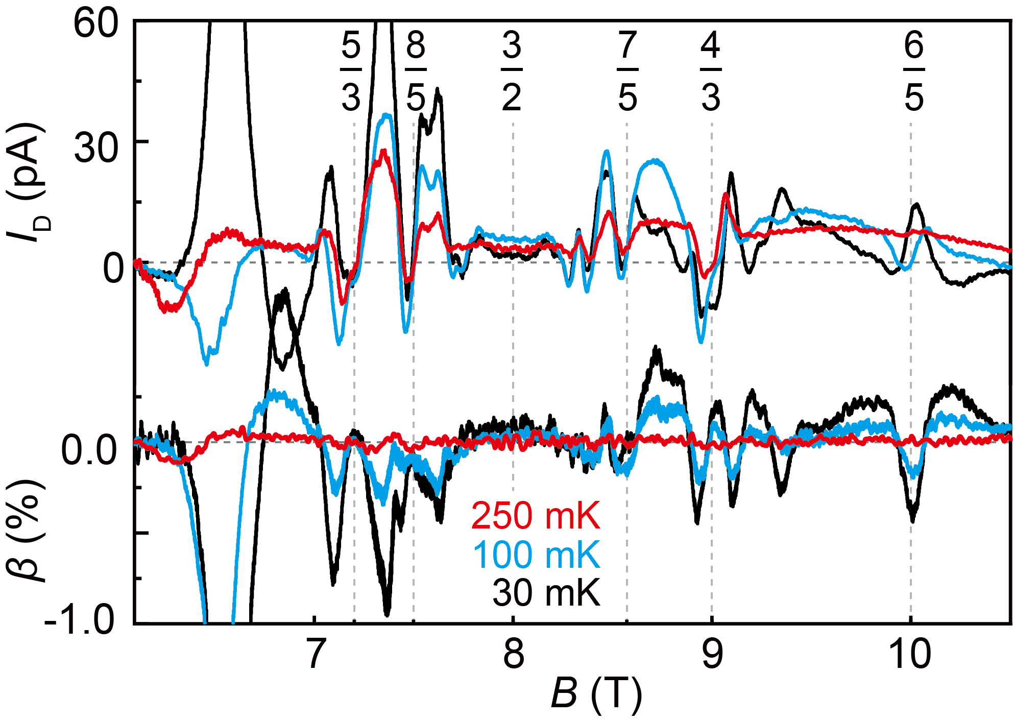
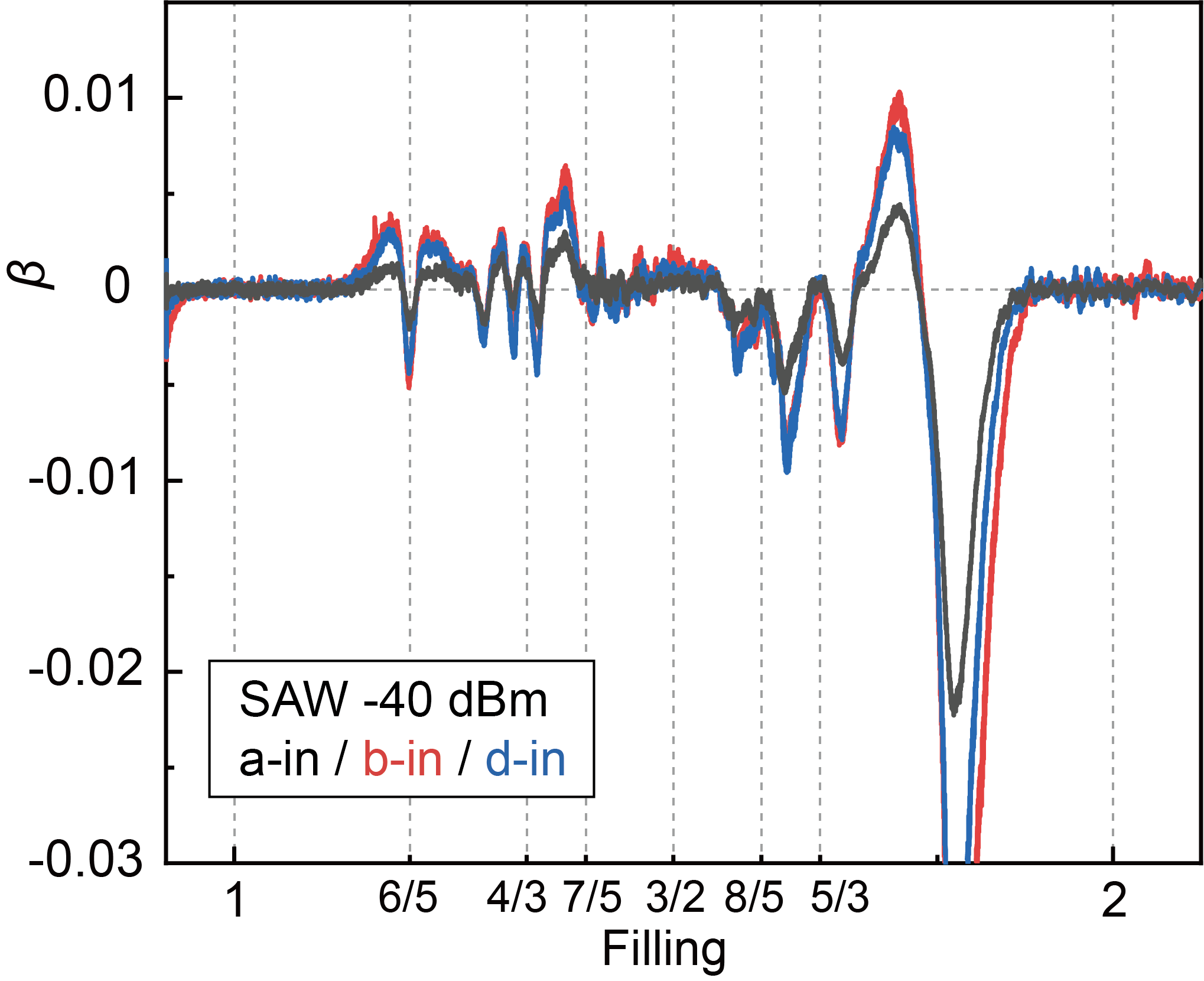
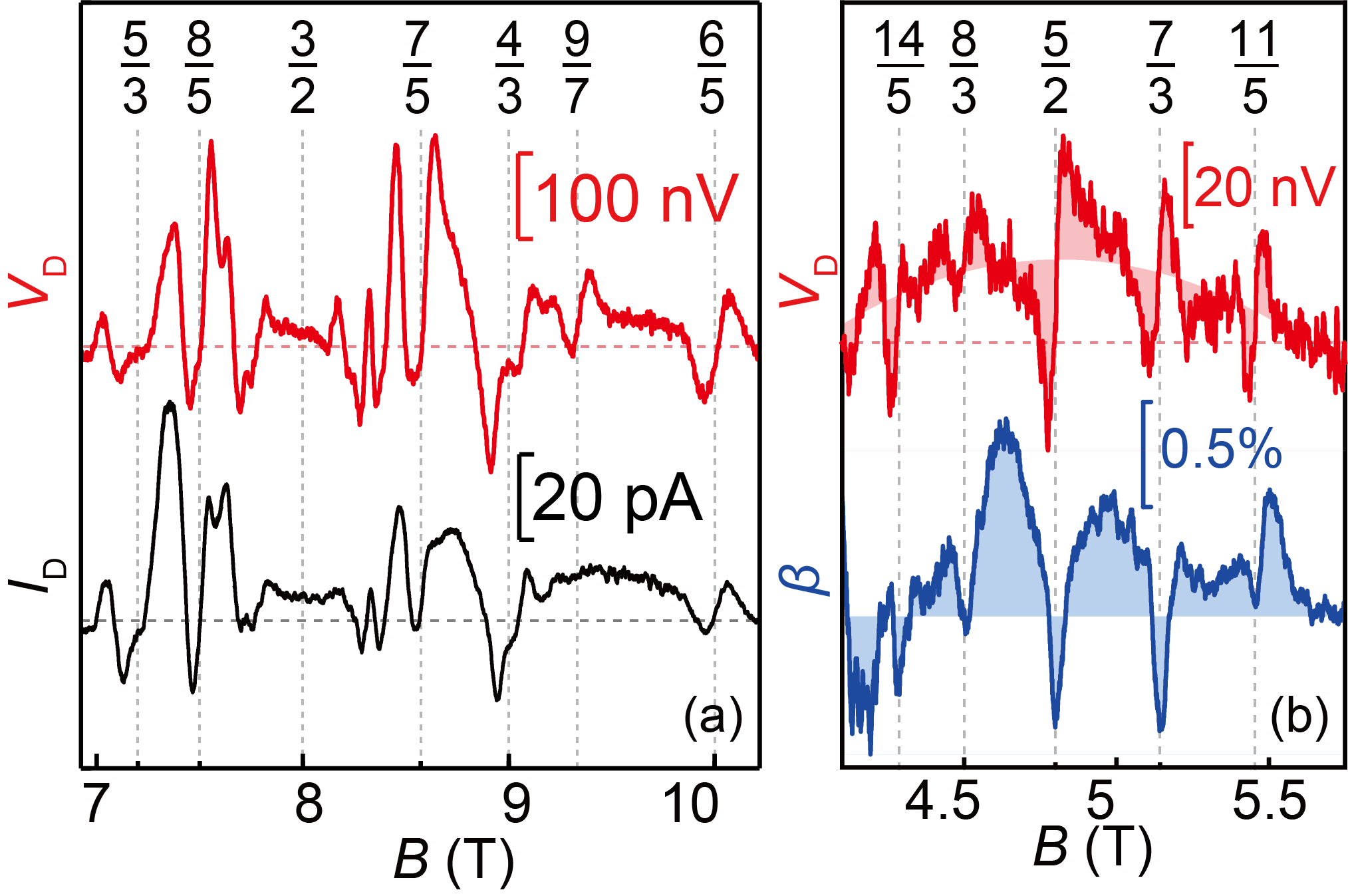
Figure 2(f) shows measured at using dBm. is also close to zero near . At strong fractional quantum Hall effects such as 5/3 and 4/3 as well as the integer quantum Hall effects at , returns to zero at exact fillings, and exhibits two negative peaks at the edge of the plateau, marked by black dots in Fig. 2(f). At weak quantum Hall effects such as =6/5 and 9/7 where has no plateau, develops one single negative peak. In short, the peaks mark the collapse of quantum Hall plateaus.
The bias current is kept below 200 pA, so that the scattering current becomes comparable with the pA when dBm. We can eliminate the scattering effect by measuring the open-loop voltage when there’s no current flowing through the sample ( pA). In this geometry, the charge accumulation at the upper and lower edge of the mesa generates an electric field to compensate the momentum transferred from the phonons. The measured open loop voltage between the two contacts is expected to be proportional to the close loop current through , where is the resistance between the two contacts. Fig. 3(a) shows measured between contacts 1 and 2 at dBm . It is nearly identical to the measured with dBm. Such an excitation level is sufficiently low, so that we are able to observe clear bipolar features in and minima in that corresponds to fragile quantum Hall effects at and 7/3, 8/3, 11/5 and 14/5; see Fig. 3(b).
A theoretical investigation of the drag and scattering effect is still missing, therefore, it is important to describe the experimentally observed features [51]. Firstly, is an odd function of quasiparticle filling factor 222The quasiparticle/quasihole filling is for integer quantum Hall effects at integer filling , and for fractional quantum Hall effect at composite Fermion filling factor ; and are integers. The relation between electron filling factor and composite Fermion filling factor is . and has opposite sign at the two flanks of quantum Hall effects, while is an even function of and its two peaks flanking the quantum Hall effect are both negative. Secondly, the peaks appear within the plateaus at , and the peaks appears at the edge of the plateaus where . Thirdly, the polarity of depends on the direction of SAW, while remains the same for all SAW propagation direction. Finally, and have different dependence on temperature . Fig. 4 shows and taken with dBm at different . As increases, weakens and completely vanishes to zero at 250 mK. remains finite up to 250 mK although its bipolar features gradually disappear.
In conclusion, we investigate the SAW-induced current in an ultra-high mobility 2DES. We find that the current response is a superposition of both drag and scattering current. We observe anomalously large bipolar peaks in drag current/voltage at quantum Hall effects, a strong evidence for the interaction between phonon and quasiparticles/quasiholes. By reducing the SAW power to orders of magnitudes lower than previous studies, we are able to investigate phases ranging from strong integer quantum Hall effects to the fragile fractional quantum Hall effects at .
Acknowledgements.
We acknowledge support by the National Key Research and Development Program of China (Grant No. 2021YFA1401900) and the National Natural Science Foundation of China (Grant No. 12074010 12141001) for sample fabrication and measurement. The Princeton University portion of this research is funded in part by the Gordon and Betty Moore Foundation’s EPiQS Initiative, Grant GBMF9615.01 to Mansour Shayegan and Loren Pfeiffer. We thank Steve Simon for valuable discussions.References
- Klitzing et al. [1980] K. v. Klitzing, G. Dorda, and M. Pepper, New method for high-accuracy determination of the fine-structure constant based on quantized hall resistance, Phys. Rev. Lett. 45, 494 (1980).
- Tsui et al. [1982] D. C. Tsui, H. L. Stormer, and A. C. Gossard, Two-dimensional magnetotransport in the extreme quantum limit, Phys. Rev. Lett. 48, 1559 (1982).
- Prange and Girvin [1987] R. E. Prange and S. M. Girvin, eds., The Quantum Hall Effect (Springer, New York, 1987).
- Jain [2007] J. K. Jain, Composite Fermions (Cambridge University Press, Cambridge, UK, 2007).
- Willett et al. [1987] R. L. Willett, J. P. Eisenstein, H. L. Störmer, D. C. Tsui, A. C. Gossard, and J. H. English, Observation of an even-denominator quantum number in the fractional quantum hall effect, Phys. Rev. Lett. 59, 1776 (1987).
- Nayak et al. [2008] C. Nayak, S. H. Simon, A. Stern, M. Freedman, and S. Das Sarma, Non-abelian anyons and topological quantum computation, Rev. Mod. Phys. 80, 1083 (2008).
- Roddaro et al. [2003] S. Roddaro, V. Pellegrini, F. Beltram, G. Biasiol, L. Sorba, R. Raimondi, and G. Vignale, Nonlinear quasiparticle tunneling between fractional quantum hall edges, Phys. Rev. Lett. 90, 046805 (2003).
- Miller et al. [2007] J. B. Miller, I. P. Radu, D. M. Zumbühl, E. M. Levenson-Falk, M. A. Kastner, C. M. Marcus, L. N. Pfeiffer, and K. W. West, Fractional quantum hall effect in a quantum point contact at filling fraction 5/2, Nature Physics 3, 561 (2007).
- Radu et al. [2008] I. P. Radu, J. B. Miller, C. M. Marcus, M. A. Kastner, L. N. Pfeiffer, and K. W. West, Quasi-particle properties from tunneling in the = 5/2 fractional quantum hall state, Science 320, 899 (2008).
- Fu et al. [2016] H. Fu, P. Wang, P. Shan, L. Xiong, L. N. Pfeiffer, K. West, M. A. Kastner, and X. Lin, Competing = 5/2 fractional quantum hall states in confined geometry, Proc. Natl. Acad. Sci. 113, 12386 (2016).
- Willett et al. [2009] R. L. Willett, L. N. Pfeiffer, and K. W. West, Measurement of filling factor 5/2 quasiparticle interference with observation of charge e/4 and e/2 period oscillations, Proc. Natl. Acad. Sci. 106, 8853 (2009).
- Zhang et al. [2009] Y. Zhang, D. T. McClure, E. M. Levenson-Falk, C. M. Marcus, L. N. Pfeiffer, and K. W. West, Distinct signatures for coulomb blockade and aharonov-bohm interference in electronic fabry-perot interferometers, Phys. Rev. B 79, 241304 (2009).
- Willett et al. [2010] R. L. Willett, L. N. Pfeiffer, and K. W. West, Alternation and interchange of e/4 and e/2 period interference oscillations consistent with filling factor 5/2 non-abelian quasiparticles, Phys. Rev. B 82, 205301 (2010).
- Nakamura et al. [2020] J. Nakamura, S. Liang, G. C. Gardner, and M. J. Manfra, Direct observation of anyonic braiding statistics, Nature Physics 16, 931 (2020).
- Saminadayar et al. [1997] L. Saminadayar, D. C. Glattli, Y. Jin, and B. Etienne, Observation of the fractionally charged laughlin quasiparticle, Phys. Rev. Lett. 79, 2526 (1997).
- de Picciotto et al. [1997] R. de Picciotto, M. Reznikov, M. Heiblum, V. Umansky, G. Bunin, and D. Mahalu, Direct observation of a fractional charge, Nature 389, 162 (1997).
- Bid et al. [2010] A. Bid, N. Ofek, H. Inoue, M. Heiblum, C. L. Kane, V. Umansky, and D. Mahalu, Observation of neutral modes in the fractional quantum hall regime, Nature 466, 585 (2010).
- Dolev et al. [2010] M. Dolev, Y. Gross, Y. C. Chung, M. Heiblum, V. Umansky, and D. Mahalu, Dependence of the tunneling quasiparticle charge determined via shot noise measurements on the tunneling barrier and energetics, Phys. Rev. B 81, 161303 (2010).
- Chickering et al. [2013] W. E. Chickering, J. P. Eisenstein, L. N. Pfeiffer, and K. W. West, Thermoelectric response of fractional quantized hall and reentrant insulating states in the landau level, Phys. Rev. B 87, 075302 (2013).
- Banerjee et al. [2017] M. Banerjee, M. Heiblum, A. Rosenblatt, Y. Oreg, D. E. Feldman, A. Stern, and V. Umansky, Observed quantization of anyonic heat flow, Nature 545, 75 (2017).
- Banerjee et al. [2018] M. Banerjee, M. Heiblum, V. Umansky, D. E. Feldman, Y. Oreg, and A. Stern, Observation of half-integer thermal hall conductance, Nature 559, 205 (2018).
- Wixforth et al. [1986] A. Wixforth, J. P. Kotthaus, and G. Weimann, Quantum oscillations in the surface-acoustic-wave attenuation caused by a two-dimensional electron system, Phys. Rev. Lett. 56, 2104 (1986).
- Wixforth et al. [1989] A. Wixforth, J. Scriba, M. Wassermeier, J. P. Kotthaus, G. Weimann, and W. Schlapp, Surface acoustic waves on gaas/as heterostructures, Phys. Rev. B 40, 7874 (1989).
- Willett et al. [1990] R. L. Willett, M. A. Paalanen, R. R. Ruel, K. W. West, L. N. Pfeiffer, and D. J. Bishop, Anomalous sound propagation at =1/2 in a 2d electron gas: Observation of a spontaneously broken translational symmetry?, Phys. Rev. Lett. 65, 112 (1990).
- Paalanen et al. [1992] M. A. Paalanen, R. L. Willett, P. B. Littlewood, R. R. Ruel, K. W. West, L. N. Pfeiffer, and D. J. Bishop, rf conductivity of a two-dimensional electron system at small landau-level filling factors, Phys. Rev. B 45, 11342 (1992).
- Willett et al. [1993] R. L. Willett, R. R. Ruel, K. W. West, and L. N. Pfeiffer, Experimental demonstration of a fermi surface at one-half filling of the lowest landau level, Phys. Rev. Lett. 71, 3846 (1993).
- Shilton et al. [1995a] J. M. Shilton, D. R. Mace, V. I. Talyanskii, M. Pepper, M. Y. Simmons, A. C. Churchill, and D. A. Ritchie, Effect of spatial dispersion on acoustoelectric current in a high-mobility two-dimensional electron gas, Phys. Rev. B 51, 14770 (1995a).
- Simon [1996] S. H. Simon, Coupling of surface acoustic waves to a two-dimensional electron gas, Phys. Rev. B 54, 13878 (1996).
- White and Voltmer [1965] R. M. White and F. W. Voltmer, Direct piezoelectric coupling to surface elastic waves, Applied Physics Letters 7, 314 (1965).
- Willett et al. [2002] R. L. Willett, K. W. West, and L. N. Pfeiffer, Experimental demonstration of fermi surface effects at filling factor 5/2, Phys Rev Lett 88, 066801 (2002).
- Friess et al. [2018] B. Friess, V. Umansky, K. von Klitzing, and J. H. Smet, Current flow in the bubble and stripe phases, Phys Rev Lett 120, 137603 (2018).
- Friess et al. [2020] B. Friess, I. A. Dmitriev, V. Umansky, L. Pfeiffer, K. West, K. von Klitzing, and J. H. Smet, Acoustoelectric study of microwave-induced current domains, Phys. Rev. Lett. 124, 117601 (2020).
- Friess et al. [2017] B. Friess, Y. Peng, B. Rosenow, F. von Oppen, V. Umansky, K. von Klitzing, and J. H. Smet, Negative permittivity in bubble and stripe phases, Nature Physics 13, 1124 (2017).
- Drichko et al. [2011] I. L. Drichko, I. Y. Smirnov, A. V. Suslov, and D. R. Leadley, Acoustic studies of ac conductivity mechanisms in -gaas/alxga1-xas in the integer and fractional quantum hall effect regime, Phys. Rev. B 83, 235318 (2011).
- Drichko et al. [2016] I. L. Drichko, I. Y. Smirnov, A. V. Suslov, Y. M. Galperin, L. N. Pfeiffer, and K. W. West, Melting of wigner crystal in high-mobility -gaas/algaas heterostructures at filling factors : Acoustic studies, Phys. Rev. B 94, 075420 (2016).
- Fang et al. [2023] Y. Fang, Y. Xu, K. Kang, B. Davaji, K. Watanabe, T. Taniguchi, A. Lal, K. F. Mak, J. Shan, and B. J. Ramshaw, Quantum oscillations in graphene using surface acoustic wave resonators, Phys. Rev. Lett. 130, 246201 (2023).
- Esslinger et al. [1992] A. Esslinger, A. Wixforth, R. Winkler, J. Kotthaus, H. Nickel, W. Schlapp, and R. Lösch, Acoustoelectric study of localized states in the quantized hall effect, Solid State Communications 84, 939 (1992).
- Esslinger et al. [1994] A. Esslinger, R. Winkler, C. Rocke, A. Wixforth, J. Kotthaus, H. Nickel, W. Schlapp, and R. Lösch, Ultrasonic approach to the integer and fractional quantum hall effect, Surface Science 305, 83 (1994).
- Shilton et al. [1995b] J. M. Shilton, D. R. Mace, V. I. Talyanskii, M. Y. Simmons, M. Pepper, A. C. Churchill, and D. A. Ritchie, Experimental study of the acoustoelectric effects in gaas-algaas heterostructures, Journal of Physics: Condensed Matter 7, 7675 (1995b).
- Rampton et al. [1996] V. Rampton, M. Ellis, P. Hennigan, I. Kennedy, C. Mellor, and M. Henini, The acousto-electric effect in the 2-d hole system using saw, Physica B: Condensed Matter 219-220, 22 (1996), pHONONS 95.
- Kennedy et al. [1998] I. Kennedy, V. Rampton, C. Mellor, B. Bracher, M. Henini, Z. Wasilewski, and P. Coleridge, Composite fermion signature in the acoustoelectric effect in 2des and 2dhs, Physica B: Condensed Matter 249-251, 36 (1998).
- Rotter et al. [1998] M. Rotter, A. Wixforth, W. Ruile, D. Bernklau, and H. Riechert, Giant acoustoelectric effect in GaAs/LiNbO3 hybrids, Applied Physics Letters 73, 2128 (1998).
- Dunford et al. [2002a] R. Dunford, M. Gates, C. Mellor, V. Rampton, J. Chauhan, J. Middleton, and M. Henini, The acoustoelectric effect in double layer algaas/gaas 2d hole systems, Physica E: Low-dimensional Systems and Nanostructures 12, 462 (2002a), proceedings of the Fourteenth International Conference on the Ele ctronic Properties of Two-Dimensional Systems.
- Dunford et al. [2002b] R. Dunford, M. Gates, C. Mellor, V. Rampton, J. Chauhan, J. Middleton, and M. Henini, Surface acoustic wave comparison of single and double layer algaas/gaas 2d hole systems, Physica B: Condensed Matter 316-317, 219 (2002b), proceedings of the 10th International Conference on Phonon Scatte ring in Condensed Matter.
- Miseikis et al. [2012] V. Miseikis, J. E. Cunningham, K. Saeed, R. O’Rorke, and A. G. Davies, Acoustically induced current flow in graphene, Applied Physics Letters 100, 133105 (2012).
- Bandhu et al. [2013] L. Bandhu, L. M. Lawton, and G. R. Nash, Macroscopic acoustoelectric charge transport in graphene, Applied Physics Letters 103, 133101 (2013).
- Zhao et al. [2020] P. Zhao, L. Tiemann, H. K. Trieu, and R. H. Blick, Acoustically driven Dirac electrons in monolayer graphene, Applied Physics Letters 116, 103102 (2020).
- Zhao et al. [2022] P. Zhao, C. H. Sharma, R. Liang, C. Glasenapp, L. Mourokh, V. M. Kovalev, P. Huber, M. Prada, L. Tiemann, and R. H. Blick, Acoustically induced giant synthetic hall voltages in graphene, Phys. Rev. Lett. 128, 256601 (2022).
- Note [1] All doping layers underneath the IDTs are removed by wet etching to avoid unwanted signal coupling. The typical attenuation of our delay-line device is approximately - 30 dB.
- Wu et al. [2024] M. Wu, X. Liu, R. Wang, Y. J. Chung, A. Gupta, K. W. Baldwin, L. Pfeiffer, X. Lin, and Y. Liu, Probing quantum phases in ultra-high-mobility two-dimensional electron systems using surface acoustic waves, Phys. Rev. Lett. 132, 076501 (2024).
- [51] See supplementary material for more information.
- Fal’ko et al. [1993] V. I. Fal’ko, S. V. Meshkov, and S. V. Iordanskii, Acoustoelectric drag effect in the two-dimensional electron gas at strong magnetic field, Phys. Rev. B 47, 9910 (1993).
- von Oppen et al. [2001] F. von Oppen, S. H. Simon, and A. Stern, Oscillating sign of drag in high landau levels, Phys. Rev. Lett. 87, 106803 (2001).
- Note [2] The quasiparticle/quasihole filling is for integer quantum Hall effects at integer filling , and for fractional quantum Hall effect at composite Fermion filling factor ; and are integers. The relation between electron filling factor and composite Fermion filling factor is .
Anomalous acousto-current within the quantum Hall plateaus
Renfei Wang Xiao Liu Mengmeng Wu
Yoon Jang Chung Adbhut Gupta Kirk W. Baldwin Mansour Shayegan Loren Pfeiffer
Xi Lin
Yang Liu
I Supplementary Materials
I.1 Sample Information and measurement setup
Our sample is an ultra-high mobility 2DES confined in 30-nm-wide GaAs/AlGaAs quantum well grown by molecular beam epitaxy. The photo of sample is shown in Fig.S1. The Van der Pauw mesa is a square with a side length of 1.2 mm. And four 5 m-period interdigital transducers (IDTs) are evaporated outside of the mesa. All doping layers underneath the IDTs are removed by wet etching to avoid unwanted signal coupling. After all these sample fabrications, the typical attenuation of our delay-line device is approximately - 30 dB.
SAW propagates along the crystal direction. The large peaks seen at 9/2, 11/2, etc. shown in Fig.2(b) of the manuscript suggest that the hard axis of these unidirectional charge density waves is along the SAW propagating direction.
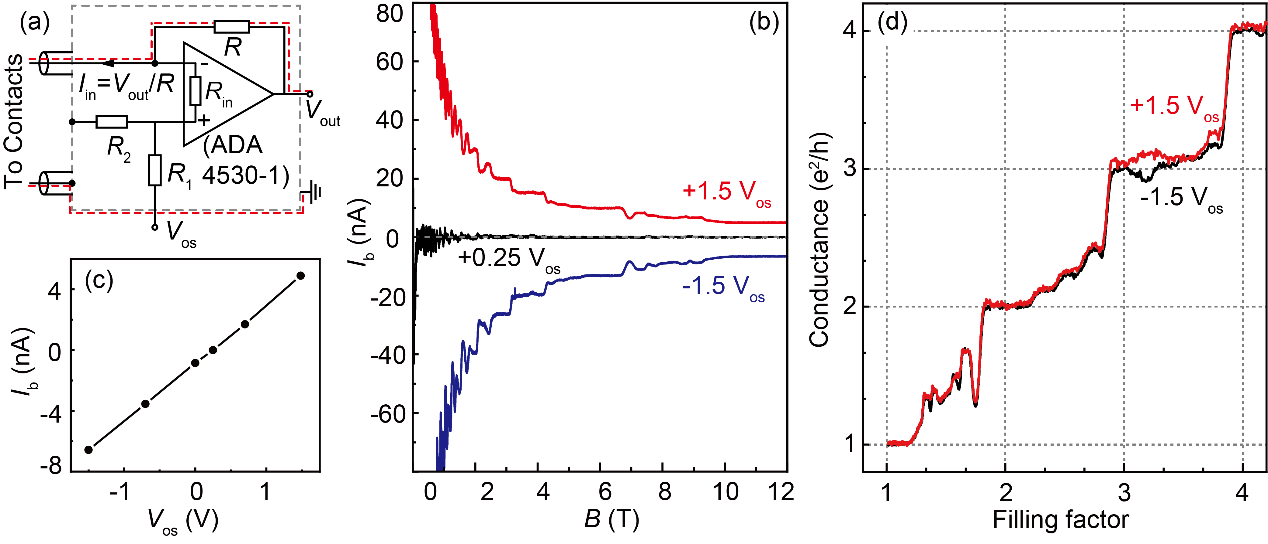
We use operational amplifier (OPA) ADA4530 to build the compact trans-impedance amplifier (TIA) for current measurement, as shown in Fig.S2(a). This particular OPA has an extremely low leak current (about less than 10 fA). And the TIA input impedance in order to efficiently drain the drag current out of the sample. Combined with the usage of coaxial wires, it forces all current flowing out of the contact to pass through the feedback resistor . So the TIA output voltage is precisely proportional to the current passing through the sample. As a result, the following relationship is precisely established:
| (1) |
When configured within its linear feedback regime, the potential difference between the inverting and noninverting inputs of an ideal OPA is zero. Unfortunately, this low-leaking current OPA have a rather large input offset voltage (up to 40 V). This implies that if we simply ground the noninverting input, a DC offset voltage will be applied at the input contact which induces a finite bias current flowing into the sample. Therefore, we incorporate a voltage divider circuit ( = 100 k, = 10 ) at the noninverting input in order to adjust . Subsequently, we measure the TIA output voltage to monitor the current through the sample. The measured DC current components for different Vos are displayed in Fig.S2(b).
The magnitudes of the current at position =1 with different is shown in Fig.S2(c). From these current and the applied we can deduce the two-point resistance of the sample using the following relation:
| (2) |
where is the voltage divider ratio and B is the input offset voltage of the OPA. From the linear relation between and in Fig.S2(c), we can derive the sample’s 2-point resistance k and the OPA’s input offset voltage (zero current) = 22.9 V. It is consistent with the fact that the two-point resistance at is almost precisely k if the contact and wire resistance is small.
The two-point conductance of the sample as a function of filling factor is obtained using Eq.(2) and shown in Fig.S2(d). The quantization of conductance occurs at integer and fractional fillings confirms the accuracy of our TIA.
In summary, our TIA enables precise monitoring of sample current with negligible leaking. We can introduce a bias voltage onto the sample contact and simultaneously measure the bias current, while employing lock-in technique to measure the AC current induced by amplitude-modulated SAW.
I.2 Two methods for obtaining the drag and scattering current
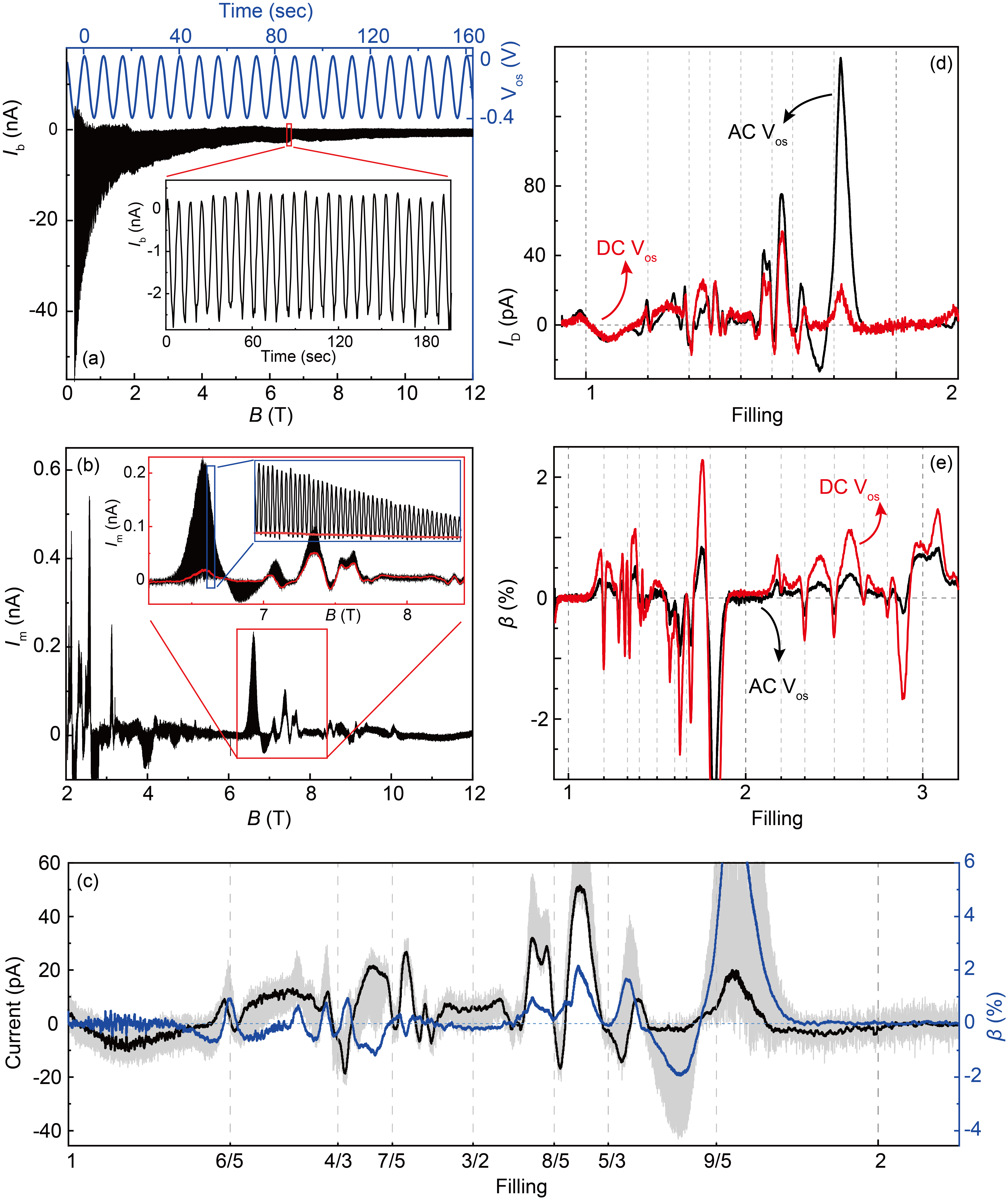
SAW induced current consists of two parts, the SAW drag and the SAW scattering , which can be separated using measured at different bias current . We have mentioned that has a linear dependence on by the equation:
| (3) |
The SAW drag is the when there is no bias current flowing through the sample and . We have two methods for deducing and . Firstly, we can calculate and using linear combination of measured with different through the flowing equations:
| (4) |
| (7) |
This approach will be quoted as the DC- procedure.
The second method, referred as AC- procedure, is applying an extremely low frequency (ten times smaller than the SAW modulation frequency) AC :
| (8) |
Therefore, we have:
| (11) |
In our experiment, we vary between 0 and -0.4 V. The applied Vos and the measured are shown in Fig.S3(a) and the is shown in Fig.S3(b). We show the by the red traces in Fig.S3(b).
Using lock-in technique, we can deduce from the TIA output, and from the oscillating component of measured , and then deduce by subtracting the scattering contribution . The results of the raw , and are shown in Fig.S3(c) using gray, black and blue curves, respectively. The and obtained from the above two methods are consistent with each other, as shown in Fig.S3(d-e).
I.3 Comparison of Bipolar drag current peaks with the SAW velocity shift
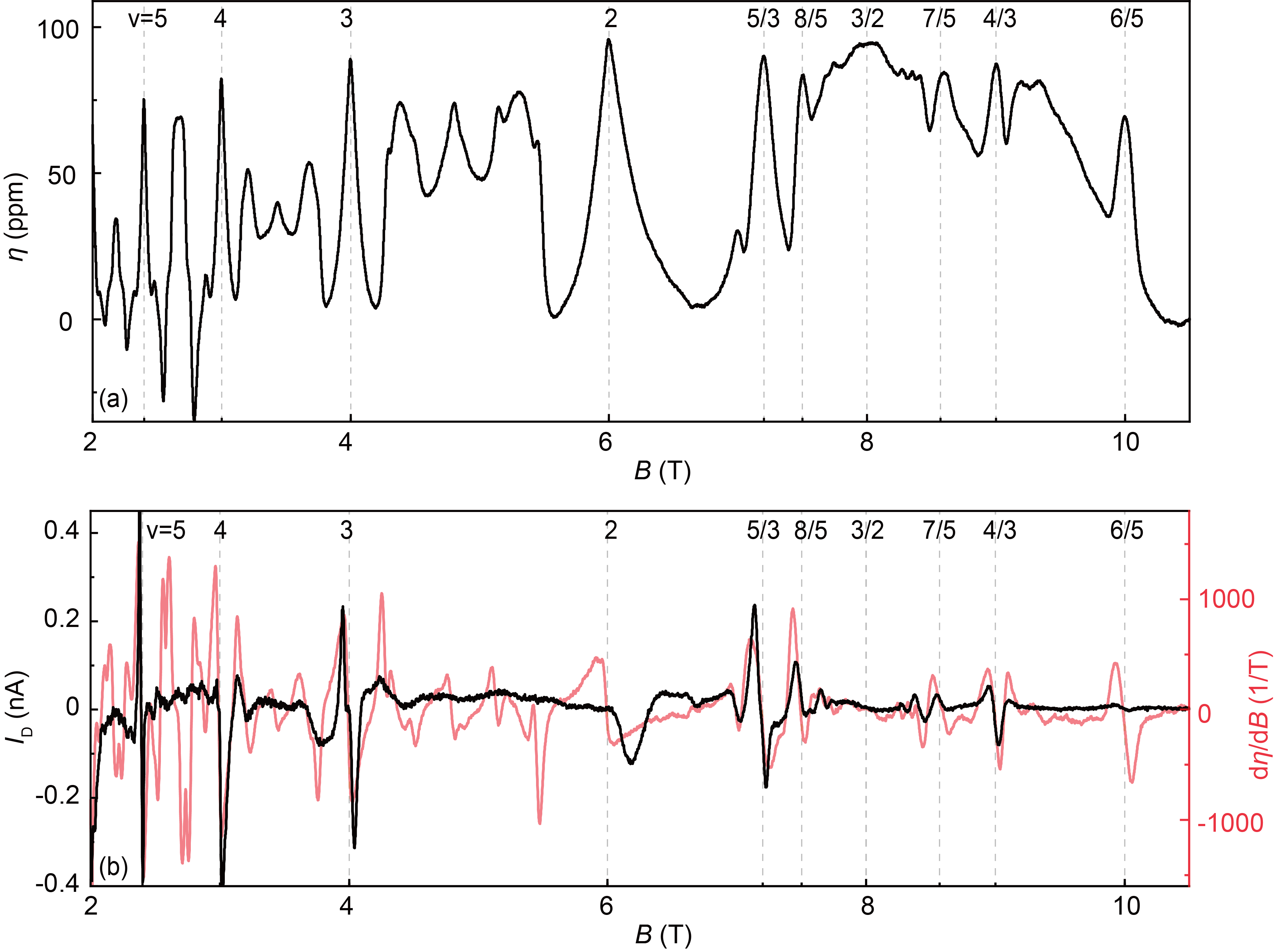
In a schematic model, the drag current can be express as:
| (12) |
In this model, the DC drag current induced by SAW is proportional to . The measured velocity shift cited from reference [50] is shown in Fig.S4(a). It is generally believed that the bulk conductivity is the reason of this velocity shift. We take the first derivative of () and compare it with the drag current in Fig.S4(b). exhibits a V-shape peak and discontinuity at exact fillings in its first derivative, which is consistent with the presence of large bipolar values of . The similarity between and the is surprisingly good in fractional states. However, the broad peaks of around integer filling fill the entire plateaus, whereas the peaks are narrower. Additionally, has rich features at stripe phases and bubble phases, etc., while the only shows peaks within a narrow range around integer quantum Hall plateaus. It is suggestive that the appearance of bipolar peaks may be related to the existence of Wigner crystal. However, as of now, there is no detailed theoretical explanation available.
I.4 The position of the drag current peaks
The peaks are observed within the Rxx plateaus at . We define for integer filling. At odd filling, peaks at positive and negative are seen in Fig.S5(a). However, the positive- peaks disappear at even filling in Fig.S5(b). This might because that the single particle gap at positive of even filling is while it is at odd fillings.
I.5 The impact of SAW direction on current
The SAW transforms the momentum to the carriers, resulting in a drag current. The polarity of this drag current flips when the SAW direction is reversed; see Fig.1(b) and 2(c) in the main text. The SAW also modulate the conductivity of the sample. The resulting scattering current is independent of the SAW propagation direction, see Fig.S6.