Anisotropic Photon Emission Enhancement near Carbon Nanotube Metasurfaces
Abstract
We present a theoretical study of the directionality effects in spontaneous emission and resonance fluorescence of a quantum two-level dipole emitter near an ultrathin closely packed periodically aligned single-wall carbon nanotube film. Such films present an example of highly anisotropic flexible metasurfaces that are now available experimentally. The nanotube alignment is shown to provide an extra measure for quantum control of dipolar spontaneous emission and resonance fluorescence in such systems, in addition to film thickness and composition parameters such as tube diameter, chirality and translational period. The processes studied are shown to be highly anisotropic, being enhanced by orders of magnitude in the direction perpendicular to the alignment and metasurface plane, contrasting with the commonly believed viewpoint of their uncontrollably random directionality.
I Introduction
A carbon nanotube (CN) is a graphene sheet rolled into a cylinder such that its length far exceeds its diameter of a few nanometers [1, 2, 3]. Its helical and translational symmetries are specified with two chiral indices that indicate how the edges of the graphene lattice are bonded at the seam. These symmetries in turn establish the tube’s axial electrical conductivity, which can range from metallic to semiconducting. Properties of CNs may be tuned by adjusting their diameter, chirality and, as with other semiconductors, by doping. While this tunability makes CNs highly effective on their own in areas ranging from electron transport [4, 5, 6] to spectroscopy related electromagnetic (EM) response phenomena [9, 7, 8, 10, 11, 12, 13, 14, 15, 16, 17, 18, 19, 20, 21, 22], it also compels their use in composite transdimensional (TD) material systems such as planar periodic arrays and films [23, 25, 24, 27, 26, 27, 28, 29, 30, 31, 32, 33]. TD quantum materials are ultrathin films made of precisely controlled number of monolayers [34, 35]. Whereas three-dimensional (3D) bulk materials allow for higher free carrier concentration and their two-dimensional (2D) counterparts such as graphene and monolayer transition metal dichalcogenides provide the strong confinement of exciton-polariton and plasmon modes [36, 37, 38], the advantages of both of these extremes can be merged by using TD materials [39, 40, 41, 42, 43, 44, 45, 46, 47, 48, 49]. For periodic CN arrays and films, in addition to controlling their thickness, new tunable attributes emerge: tube-diameter-to-film-thickness ratio, intertube spacing, and abundance ratio of tube geometries in the array assortment [51, 52, 53, 50, 54].
In recent years, modern fabrication techniques have appreciably improved the quality of CN films [55, 56, 57]. This has led to a myriad of diverse applications such as single-photon sources [7, 58, 59, 60, 61, 62], field effect transistors [25, 24], rechargeable batteries [63], electrothermal actuators [64], electron [65] and thermal [26] transport control, supercapacitors [66], solar cells [67]—even directional dark matter detection [68] and agriculture [69]—to name a few. A significant sector of current TD materials research is committed to experiment and theory to study self-assembled thin films of periodically aligned single-wall carbon nanotube (SWCN) arrays [26, 27, 28, 29, 30]—a new highly anisotropic TD material platform for designing efficient flexible unidirectional hyperbolic metasurfaces (MSs) with characteristics adjustable on demand by means of their thickness, SWCN diameter, chirality, and periodicity variation. It was recently shown experimentally [29] and explained theoretically [50] that in the SWCN alignment direction the real part of the linear EM response function of the ultrathin single-type CN array has a broad negative refraction (NR) band near a quantum interband transition of the constituent SWCN, whereby the film behaves as an in-plane anisotropic (unidirectional) hyperbolic MS at much higher frequencies than those (typically in the IR [70]) that classical plasma oscillations have to offer. By decreasing the CN diameter it is possible to push this NR band into the visible range and using weakly inhomogeneous doped multitype SWCN films broadens the NR bandwidth [50], to allow both near- and far-field interaction control in the SWCN array systems [51, 52, 53].
In the present work, our focus is on spontaneous emission (SE) and fluorescence of atoms (or molecules) in close proximity to a finite-thickness ultrathin film of periodically aligned densely-packed SWCNs, as sketched in Fig. 1. This in-plane anisotropic MS is assumed to be in the TD regime where its in-plane-anisotropic EM response is effectively 2D while still retaining thickness to represent the out-of-plane film size [50]. Such TD films like that can be used as highly-selective optical and infrared sensors for single atom or molecule detection, trapping, and manipulation [12, 71], including molecular chemical reactivity control [72]. We study theoretically both near-field SE and far-field resonance fluorescence by atomic type dipole emitters (DE) in these systems, focusing on the anisotropic photon emission enhancement effects. While SE rate variation have been previously investigated for a variety of nanosystems, such as single SWCNs [73, 22], plasmonic nanocavities [44, 72, 74], and photonic crystals [75, 76, 77], the directionality effects in SE, resonance fluorescence and scattering of light by quantum DEs near in-plane anisotropic TD metasurfaces still require proper theoretical attention.

We use a fully quantized medium-assisted Quantum Electrodynamics (QED) approach [78], with SE and fluorescence generated by an excited two-level DE in close proximity to an ultrathin closely-packed SWCN film, a particular case of the in-plane anisotropic TD optical MS. In such systems, the confinement-induced EM response nonlocality is known to play a crucial role and no semiclassical theory of EM wave propagation is expected to work [79]. TD materials restructure the spectral and spatial distribution of EM modes pertaining to not only real but also virtual vacuum processes such as SE and van der Waals coupling [44, 51]. While the real modes can be described semiclassically, the physical consequences of the vacuum restructuring with new EM modes generated spontaneously can only be understood in terms of a fully quantized medium-assisted QED formalism [80, 81]. Semiclassical results are identical to those of QED for processes like single-photon absorption where no modes are spontaneously generated in the process [80]. Converse examples are dipolar SE enhancement due to the DE coupling to the TD epsilon-near-zero modes [44, 41] and interatomic Coulomb decay [82], studied recently within the framework of medium-assisted QED, to yield decay rates orders of magnitude greater than those expected semiclassically.
We develop the QED theory to show that the SWCN periodic parallel alignment provides an extra measure for the SE and resonance fluorescence control of the quantum DE near the SWCN metasurface—in addition to the MS thickness and composition parameters such as SWCN diameter, chirality and translational period. The dipolar SE rate and photon fluorescence intensity exhibit highly anisotropic behavior, being enhanced by orders of magnitude in the plane perpendicular to the SWCN alignment along the direction perpendicular to the MS plane, in contrast to the commonly believed viewpoint of their uncontrollably random directionality. The following sections describe our model, present our theoretical results, and conclude our work by summarizing its key findings. The details of the most cumbersome calculations are described in the two appendices at the end.
II Medium-Assisted QED Formalism for Transdimensional Metasurfaces
In the medium-assisted QED approach we use here for the TD optical MSs of thickness that are made of ultrathin densely packed periodic SWCN arrays, intrinsic quasiparticle (phonon, plasmon, exciton, etc.) relaxation phenomena started by absorption of light are considered to create random field fluctuations superposed on those of the physical vacuum (no medium present). These medium-assisted fluctuating vacuum-type EM fields can be represented by the quantum electric and magnetic field operators (Schrödinger picture, Gaussian units)
| (1) | |||
| (2) |
Their respective Fourier-image vector components are (, )
| (3) | |||
| (4) | |||
| (5) |
Medium composition is included in this QED equation set by means of the imaginary part of the EM response tensor . This tensor is assumed to be diagonal and independent of the vertical -coordinate, which for ultrathin optically dense TD films is represented by thickness of the film [48, 47, 44]. Medium confinement geometry is defined by the classical EM field Green’s tensor , which can be found for a confined material system of interest under appropriate boundary conditions and radiation conditions at infinity [78, 83]. The operator is the Fourier-image of the noise current density operator responsible for medium absorption whereby single-quantum vacuum-type medium excitations are created (annihilated) by bosonic operators () such that
| (6) |
The presence of the noise current density operator is consistent with the Fluctuation-Dissipation Theorem and is necessary to warrant the correct equal-time electric and magnetic field operator commutation relations of vacuum QED in the presence of medium absorption [78].
III Dipole emitter and metasurface: the hamiltonian
In terms of the medium-assisted QED scheme above, the following second-quantized Hamiltonian describes the coupled atom-field system with an atom (or a molecule) at an arbitrary point above the SWCN film, as sketched in Fig. 1, within the framework of the electric dipole and two-level approximations [78, 22]
| (7) | |||
Here, the three terms represent the quantum medium-assisted field subsystem, the atomic subsystem modeled by a quantum two-level DE with frequency , and their interaction, respectively. The Pauli operators , , describe the transitions in the atomic subsystem between its upper and lower states. The interaction term is due to the coupling of the atomic transition dipole () to the quantum medium-assisted electric field of Eqs. (1)–(4) where the medium composition is represented by the imaginary part of the EM response tensor of the SWCN film. Due to the van der Waals type coupling of the DE to the film, the frequency is generally red-shifted () relative to the transition dipole frequency (see, e.g., Ref. [78]).
Collective EM response of the TD films made of periodically aligned SWCN arrays was recently studied theoretically [54, 50]. With contributions from both plasmons and excitons (corresponding to intra- and interband transitions in the far-infrared and optical spectral regions, respectively), it was shown to be strongly anisotropically nonlocal due to the cylindrical spatial anisotropy, periodic in-plane transverse inhomogeneity, and vertical quantum confinement of the system. In the reciprocal (momentum) space the anisotropic EM response of such an ultrathin finite-thickness MS can be represented by the 3D tensor
| (8) |
Here, is the effective constant permittivity of the dielectric layer with the aligned SWCN array immersed in it. This is the response of the MS in the -direction perpendicular to the SWCN alignment as shown in Fig. 1. The response of the ultrathin MS structure in the -direction makes no effect on light propagation. We take it to be in what follows since the range of thicknesses does not exceed the wave length of light in the TD regime and the transverse polarizability of SWCNs is negligible. The function
| (9) |
is the nonlocal response of the TD film in the direction of SWCN alignment (-direction). Here , and are the -direction quasiparticle momentum absolute value, the volume fraction of SWCNs and the axial surface conductivity of an individual SWCN, respectively. The quantity
| (10) |
stands for the intraband plasma oscillation frequency for a general finite-thickness, cylindrically anisotropic, periodically aligned (metallic or semiconducting) array [54]. Here, is the electron effective mass, is the surface electron density, and are the zeroth-order modified cylindrical Bessel functions. The latter are responsible for the correct normalization of the electron density distribution over cylindrical surfaces, to give the isotropic TD film plasma frequency studied previously in Refs. [48, 42] in the limit (in which case ).
IV Anisotropic Spontaneous Emission
When an atomic DE is initially in the upper state and the field subsystem is in vacuum, the time-dependent wave function of the whole system can be written as
| (11) | |||
Here, is the vacuum state of the medium-assisted field subsystem, is its excited state where the field is in a single-quantum Fock state with DE oriented in the -direction, and are the population probability amplitudes of the upper state and lower state of the coupled DE-MS system such that
Plugging the wave function (11) in the time-dependent Schrödinger equation with the Hamiltonian (7), one obtains the following coupled equation set for the unknown population probability amplitudes
| (12) | |||
| (13) | |||
Substituting the result of the integration of Eq. (13) [see Eq. (41)] into Eq. (12) and using the identity
| (14) | |||
(a particular case of the general 3D Green tensor integral relation, see Ref. [78]), with initial conditions and it is finally straightforward to obtain
| (15) |
The kernel of this integral (Volterra) equation is
| (16) |
with
| (17) |
the dipole spontaneous emission rate as a function of , written in terms of the imaginary part of the equal-position EM field Green tensor—a particular case of the tensor . The latter can be split into two parts
| (18) |
to represent the free space and MS scattering contributions, respectively.
The free space contribution of Eq. (18) comes out of the well-known EM field Green tensor of the free dielectric space,
| (19) |
where in our case and . Here, it is straightforward to perform the differentiation, followed by the 3D space averaging , to obtain
| (20) |
whereby
| (21) |
With this taken into account, Eq. (17) can be rewritten in the principle axes system of the tensor, which is dictated by the EM response tensor (8) of the MS, as follows
| (22) |
Here, is the isotropic dipolar spontaneous emission rate in the free dielectric space, with and as indicated in Fig. 1. The function
| (23) |
is the anisotropic local photonic density of states (LDOS) that includes the MS presence effect relative to vacuum.
V Resonance Fluorescence
In terms of our medium-assisted QED approach, the fluorescence intensity of an atomic DE near the SWCN metasurface can be written as
| (24) |
where the field operators are defined by Eqs. (1)–(4) with the metasurface EM response tensor of Eq. (8) and the wave function of the system given by Eq. (11). From here, using Eq. (14) and the coefficients obtained by integration of Eq. (13), it is possible to bring the intensity of interest to the final form as follows (see Appendix A)
| (25) |
where
| (26) |
In view of Eqs. (18) and (20) this can also be brought to the form
| (27) | |||
where
| (28) |
are the anisotropic distance-dependent photonic LDOS functions related to the LDOS of Eq. (23) as follows
Resonance fluorescence results from being in resonance with a peak frequency of the LDOS in Eq. (22). With the latter approximated by the Lorentzian function of half-width-at-half maximum , where , Eq. (15) can be solved analytically to yield in Eq. (25) in the following explicit form
| (29) |
Here, and the Rabi frequency is to represent the DE level hybridization due to the coupling to the quantum medium-assisted modes of the material subsystem (excitons and plasmons in the parallel aligned SWCNs of our TD metasurface). The coupling is termed weak if , in which case Eq. (29) yields the fast exponential decay time dynamics for the upper DE state, or strong if , in which case it yields slow decay dynamics with Rabi oscillations .
Using Eq. (29) inside of Eq. (27) and observing that the second (oscillatory) term in square brackets of Eq. (27) is negligible for and so can be dropped, the following expression can be obtained for sufficiently long time in this most relevant limit (see Appendix B)
| (30) | |||
with . This asymptotic long-distance, long-time expression can be simplified further to give the weak and strong DE-MS coupling cases individually. Using the first-nonvanishing-order Taylor series expansions for the coefficients in it leads to
| (31) |
and
| (32) |
for weak and strong DE-MS coupling, respectively, with
| (33) |
where . Thus, the fluorescence intensity time dynamics (fast exponential for the former and slow oscillatory for the latter) are both controlled by the largely increased anisotropic amplitude (distance-dependent photonic LDOS squared) due to the DE-MS interaction.
VI Results and Discussion
As can be seen from the above, the photonic LDOS of Eq. (23) and its distance-dependent analogue of Eq. (28) are the key quantities to control the near-field EM processes such as spontaneous emission and resonance fluorescence, respectively. Both of them are determined by the scattering part of the EM field Green tensor of a planar multilayer structure, which can be diagonalized as per the in-plane layer symmetry and can generally be factored into the in-plane and out-of-plane components [83]. The distance dependence of such a tensor is largest (and so of the most interest) in the out-of-plane direction along the -axis (see Fig. 1), where it takes the form
| (34) | |||
Here, is the in-plane momentum with absolute value , and is the absolute value of the out-of-plane momentum component in the positive direction of the -axis.
For our anisotropic single-layer case, Eq. (34) can be written in terms of the reflection coefficients for spontaneously emitted - and -polarized photons (TE and TM waves, respectively) as follows [83, 84]
| (35) | |||
where the reflection coefficients in standard notations are
| (36) | |||
according to the EM response tensor (8) of our system. Here, and are the absolute values of the photon momentum -components in region (substrate with dielectric constant ), in region (dielectric constant ) where the DE is situated, and in the -directions of the region bounded by the anisotropic MS, respectively. Rescaling of the quantities in Eq. (35) by
| (37) |
with , allows one to rewrite it as a sum of the two well-defined single-valued real integrals of the form
| (38) | |||
Here, the first and second integrals are contributed by the evanescent and propagating waves, respectively, as can be seen from the exponential factors of their integrands. It can also be seen from Eqs. (22), (23) and Eqs. (28), (33) that the former is responsible for the spontaneous emission enhancement of the DE while the latter makes strong resonance fluorescence possible for it as a two-step process ( therefore) in which most of the photons emitted spontaneously by the DE get re-emitted to infinity by the entire MS structure.

Figure 2 shows a typical example of the real and imaginary parts of the low-energy in-plane EM response function along the SWCN alignment direction (-direction in Fig. 1) for ultrathin SWCN metasurfaces, which we use in Eqs. (8)–(10) to simulate the photonic LDOS of Eq. (23) and its distance-dependent analogue of Eq. (28). This function was previously reported in Ref. [50] to have been obtained numerically from Eqs. (9) and (10) with (dielectric layer) and by using the Maxwell-Garnett method for the nm thick weakly inhomogeneous TD metasurface. The structure was comprised of a quasiperiodic mixture of the (16,0), (17,0), (18,0), (19,0) and (20,0) metallic and semiconducting SWCN arrays to make the film composition metallic and semiconducting as is normally the case experimentally [27, 28, 29, 30, 31, 32, 33]. Here, the energy range is chosen to include the first exciton resonance only. The graphs reproduce the overall EM response behavior reported for thin self-assembled SWCN films experimentally [29]. The real part (blue line) of the EM response forms a relatively broad NR band in the neighborhood of the exciton transition (brown line) to make the system behave as a uniaxial hyperbolic MS not only at low (typically IR) but also at higher frequencies right below the classical and quantum interband plasmon resonances (green line), adjustable by a proper choice of the CN content [50].
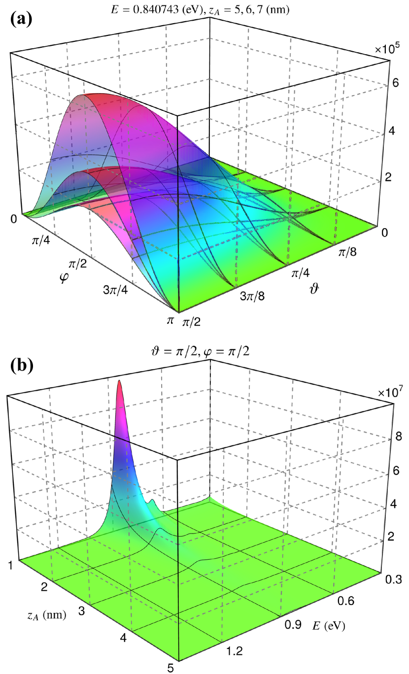
Figure 3 (a) presents the anisotropic LDOS of Eq. (23) calculated with the EM field Green tensor of Eq. (35) as a function of the transition dipole relative orientation angles as sketched in Fig. 1. The atomic DE is positioned at nm with its excitation energy chosen to be in the middle of the NR band of the function given by Eqs. (8)–(10) and presented in Fig. 2. It can be seen that the maximum of the anisotropic LDOS and the maximal SE rate, accordingly, are to be expected in the plane perpendicular to the SWCN alignment along the direction perpendicular to the MS plane, in which case the transition dipole vector of the DE is parallel to the SWCN alignment (see Fig. 1). Getting the DE closer to the film surface increases the LDOS in this particular direction, whereby the dipolar SE rate increases unidirectionally to exceed the vacuum SE rate by a factor at nm as prescribed by Eq (22). Figure 3 (b) shows the fixed-angle max LDOS [taken at per Fig. 3 (a)] as a function of the DE-MS distance and DE transition energy where, by comparison with Fig. 2, it can be seen that the NR band of the function results in the strong resonance of the LDOS with unidirectional SE rate reaching relative to vacuum for nm. This is a clear near-field effect contributed predominantly by the evanescent part of the EM field Green tensor as can be seen from Eq. (38) with .

Figure 4 shows the calculated short-distance (a) and long-distance (b) behaviors of the fixed-angle () max LDOS function of Eq. (28) for varying observation point (detector) position and DE transition energy with the DE position fixed at nm. As can be seen from Eqs. (30)–(33), it is this function that totally controls the distance and time dependences of the anisotropic resonance fluorescence intensity of an excited DE in close proximity to the MS. Both graphs are calculated with the EM field Green tensor of Eq. (35) in the form prescribed by Eq. (38) in order to be able to see the role of the evanescent and propagating wave contributions separately as the observation point moves away from the MS structure. In (a) both terms are included in the calculation, while in (b) only the propagating term is included with its sign inverted. Clearly, as prescribed by Eq. (38), the evanescent (near-field wave) contribution dominates at short (greater than ) so much that the propagating wave contribution is totally hidden and cannot even be seen in (a). However, as the observation point moves away perpendicular to the MS plane, the dominant role played by the evanescent waves close to the surface is instead taken on by their propagating counterparts at large (much greater than ) as shown in (b). Here, the anisotropic distance-dependent LDOS function oscillates and slowly decreases with increasing . So, too, does the DE anisotropic fluorescence intensity as can be seen from Eqs. (30)–(33) with , and as was first reported experimentally by Drexhage for (isotropic) atomic fluorescence intensity near a dielectric interface [85]. From the comparison of (a) and (b), the maximum of the fluorescence intensity can also be seen to broaden and shift with to the red, which is the physical red shift in addition to that already included in the DE transition frequency as described for Eq. (7) above.
VII Conclusions
We use the medium-assisted QED approach to study the directionality effects in SE and fluorescence of atoms (or molecules) in close proximity to finite-thickness ultrathin films of periodically aligned SWCNs. The latter are a particular case of TD metasurface structures with nonlocal and highly anisotropic in-plane EM response. In general, the nonlocality of the EM response is known to play a crucial role in modifying the EM properties of materials [79, 39, 40, 41, 42]. The material system we study here restructures the spectral and spatial distribution of the EM eigenmodes pertaining to both real (far-field fluorescence) and virtual (near-field SE) medium-assisted photon emission processes to enhance them unidirectionally over a broad range of atomic excitation frequencies. Specifically, in addition to the Casimir effect anisotropy reported recently [51, 52], here we show that the atomic dipolar SE rate and fluorescence intensity exhibit highly anisotropic behavior, being enhanced by orders of magnitude in the plane perpendicular to the SWCN alignment along the direction perpendicular to the MS plane, in contrast to the commonly believed viewpoint of their uncontrollably random directionality.
The results reported herein generalize those of the seminal work by Drexhage [85] as well as those of related recent works [44, 41] to show that the SWCN periodic parallel alignment provides an extra measure for the SE and resonance fluorescence control of the quantum DE located nearby, in addition to MS composition parameters and thickness. Our theoretical study thus indicates that the periodically aligned ultrathin TD films of SWCNs is an excellent platform for the development of multifunctional optical hyperbolic metasurfaces not only for IR but also for the optical spectral range. SWCN metasurfaces can be used as highly-selective optical and IR sensors for single atom or molecule detection, trapping and manipulation. This also includes solid-state atomic single-photon source device engineering, molecular chemical reactivity control and, in general, the development of the new generation of ultrathin TD materials for quantum information processing applications.
Acknowledgements.
I.V.B. gratefully acknowledges support from the U.S. Army Research Office under award No. W911NF2310206. M.D.P. and S.F.I. were supported in part by the U.S. National Science Foundation grant No. DMR-1830874 awarded to I.V.B..Appendix A Derivation of Eq. (25)
Appendix B Derivation of Eq. (30)
For given by Eq. (29) the time-dependent factor in Eq. (25) takes the form
| (42) | |||
with . For our purposes here, this can further be treated in the long-time approximation using the well-known identity [86]
( denotes the principal value), whereby Eq. (42) can be written as
| (43) | |||
Plugging Eq. (43) into Eq. (25) and observing that its final parenthesized term integrates over to zero due to the preceding alternating-sign exponential factor, one ultimately arrives at Eq. (30).
References
- [1] R.Saito, G.Dresselhaus, and M.S.Dresselhaus, Physical Properties of Carbon Nanotubes (Imperial College, 1998).
- [2] L.X.Zheng, M.J.O’Connell, S.K.Doorn, X.Z.Liao, Y.H. Zhao, E.A.Akhadov, M.A.Hoffbauer, B.J.Roop, Q.X.Jia, R.C.Dye, D.E.Peterson, S.M.Huang, J.Liu and Y.T.Zhu, Ultralong single-wall carbon nanotubes, Nature Mater. 3, 673 (2004).
- [3] M.F.L. De Volder, S.H.Tawfick, R.H.Baughman, and A.J.Hart, Carbon nanotubes: Present and future commercial applications, Science 339, 535 (2013).
- [4] K.R.Jinkins, S.M.Foradori, V.Saraswat, R.M.Jacobberger, J.H.Dwyer, P.Gopalan, A.Berson, and M.S.Arnold, Aligned 2D carbon nanotube liquid crystals for wafer-scale electronics. Science Advances 7, eabh0640 (2021).
- [5] M.F.Gelin and I.V.Bondarev, One-dimensional transport in hybrid metal-semiconductor nanotube systems, Phys. Rev. B 93, 115422 (2016).
- [6] T.Ando, Theory of electronic states and transport in carbon nanotubes, J. Phys. Soc. Jpn. 74, 777 (2005).
- [7] J.Zaumseil, Luminescent defects in single-walled carbon nanotubes for applications, Adv. Optical Mater. 10, 2101576 (2022).
- [8] W.Gao, X.Li, M.Bamba, and J.Kono, Continuous transition between weak and ultrastrong coupling through exceptional points in carbon nanotube microcavity exciton-polaritons, Nature Photonics 12, 362 (2018).
- [9] F.S.Hage, T.P.Hardcastle, A.J.Scott, R.Brydson, and Q.M.Ramasse, Momentum- and space-resolved high-resolution electron energy loss spectroscopy of individual single-wall carbon nanotubes, Phys. Rev. B 95, 195411 (2017).
- [10] I.V.Bondarev and A.Popescu, Exciton Bose-Einstein condensation in double walled carbon nanotubes, MRS Advances 2, 2401 (2017).
- [11] A.Graf, L.Tropf, Y.Zakharko, J.Zaumseil, and M.C.Gather, Near-infrared exciton-polaritons in strongly coupled single-walled carbon nanotube microcavities, Nature Communications 7, 13078 (2016).
- [12] I.V.Bondarev, Plasmon enhanced Raman scattering effect for an atom near a carbon nanotube, Opt. Express 23, 3971 (2015).
- [13] L.Martín-Moreno, F.J.García de Abajo, and F.J.García-Vidal, Ultraefficient coupling of a quantum emitter to the tunable guided plasmons of a carbon nanotube, Phys. Rev. Lett. 115, 173601 (2015).
- [14] I.V.Bondarev, Relative stability of excitonic complexes in quasi-one-dimensional semiconductors, Phys. Rev. B 90, 245430 (2014).
- [15] I.V.Bondarev and A.V.Meliksetyan, Possibility for exciton Bose-Einstein condensation in carbon nanotubes, Phys. Rev. B 89, 045414 (2014).
- [16] Q.Zhang, E.H.Hároz, Z.Jin, L.Ren, X.Wang, R.S.Arvidson, A.Lüttge, and J.Kono, Plasmonic nature of the terahertz conductivity peak in single-wall carbon nanotubes, Nano Letters 13, 5991 (2013).
- [17] I.V.Bondarev, Single-wall carbon nanotubes as coherent plasmon generators, Phys. Rev. B 85, 035448 (2012).
- [18] I.V.Bondarev, T.Antonijevic, Surface plasmon amplification under controlled exciton-plasmon coupling in individual carbon nanotubes, Phys. Stat. Sol. C 9, 1259 (2012).
- [19] A.Popescu, L.M.Woods, and I.V.Bondarev, Chirality dependent carbon nanotube interactions, Phys. Rev. B 83, 081406 (2011).
- [20] I.V.Bondarev, L.M.Woods, and K.Tatur, Strong exciton-plasmon coupling in semiconducting carbon nanotubes, Phys. Rev. B 80, 085407 (2009).
- [21] M.S.Dresselhaus, G.Dresselhaus, R.Saito, and A.Jorio, Exciton photophysics of carbon nanotubes, Ann. Rev. Phys. Chem. 58, 719 (2007).
- [22] I.V.Bondarev and P.Lambin, Near-field electrodynamics of atomically doped carbon nanotubes, in: Trends in Nanotubes Research, ed. D.A.Martin (Nova Science, NY, 2006), Ch.6, pp.139-183.
- [23] S.M.Foradori, J. H.Dwyer, A.Suresh, P.Gopalan, and M.S.Arnold, High transconductance and current density in field effect transistors using arrays of bundled semiconducting carbon nanotubes. Applied Physics Letters, 121(7), 073504 (2022).
- [24] L.Liu, J.Han, L.Xu, J.Zhou, C.Zhao, S.Ding, H.Shi, M.Xiao, L.Ding, Z.Ma, C.Jin, Z.Zhang, and L.-M.Peng, Aligned, high-density semiconducting carbon nanotube arrays for high-performance electronics, Science 368, 850 (2020).
- [25] G.J.Brady, A.J.Way, N.S.Safron, H.T.Evensen, P.Gopalan, and M.S.Arnold, Quasi-ballistic carbon nanotube array transistors with current density exceeding Si and GaAs, Science Advances 2, e1601240 (2016).
- [26] J.A.Roberts, P.-H.Ho, S.-J.Yu, and J.A.Fan, Electrically driven hyperbolic nanophotonic resonators as high speed, spectrally selective thermal radiators, Nano Letters 22, 5832 (2022).
- [27] J.A.Roberts, P.-H.Ho, S.-J.Yu, X.Wu, Y.Luo, W.L.Wilson, A.L.Falk, and J.A.Fan, Multiple tunable hyperbolic resonances in broadband infrared carbon-nanotube metamaterials, Phys. Rev. Appl. 14, 044006 (2020).
- [28] S.Schöche, P.-H.Ho, J.A.Roberts, S.J.Yu, J.A.Fan, and A.L.Falk, Mid-IR and UV-Vis-NIR mueller matrix ellipsometry characterization of tunable hyperbolic metamaterials based on self-assembled carbon nanotubes, J. Vac. Sci. Technol. B 38, 014015 (2020).
- [29] J.A.Roberts, S.-J.Yu, P.-H.Ho, S.Schöche, A.L.Falk, and J.A.Fan, Tunable hyperbolic metamaterials based on self-assembled carbon nanotubes, Nano Lett. 19, 3131 (2019).
- [30] W.Gao, C.F.Doiron, X.Li, J.Kono, and G.V.Naik, Macroscopically aligned carbon nanotubes as a refractory platform for hyperbolic thermal emitters, ACS Photonics 6, 1602 (2019).
- [31] M.E.Green, D.A.Bas, H.-Y.Yao, J.J.Gengler, R.J.Headrick, T.C.Back, A.M.Urbas, M.Pasquali, J.Kono, and T.-H.Her, Bright and ultrafast photoelectron emission from aligned single-wall carbon nanotubes through multiphoton exciton resonance, Nano Lett. 19, 158 (2019).
- [32] P.-H.Ho, D.B.Farmer, G.S.Tulevski, S.-J.Han, D.M.Bishop, L.M.Gignac, J.Bucchignano, Ph.Avouris, and A.L.Falk, Intrinsically ultrastrong plasmon-exciton interactions in crystallized films of carbon nanotubes, PNAS 115, 12662 (2018).
- [33] A.L.Falk, K.-C.Chiu, D.B.Farmer, Q.Cao, J.Tersoff, and Y.-H.Lee, Coherent Plasmon and Phonon-Plasmon Resonances in Carbon Nanotubes, Phys. Rev. Lett. 118, 257401 (2017).
- [34] A.Boltasseva and V.M.Shalaev, Transdimensional photonics, ACS Photonics 6, 1 (2019).
- [35] D.Shah, Z.Kudyshev, S.Saha, V.M.Shalaev, and A.Boltasseva, Transdimensional material platforms for tunable metasurface design, MRS Bulletin 45, 188 (2020).
- [36] D.N.Basov, M.M.Fogler, A.Lanzara, F.Wang, and Y.Zhang, Colloquium: Graphene spectroscopy, Rev. Mod. Phys. 86, 959 (2014).
- [37] K.F.Mak and J.Shan, Photonics and optoelectronics of 2d semiconductor transition metal dichalcogenides, Nature Photonics 10, 216 (2016).
- [38] F.Xia, H.Wang, D.Xiao, M.Dubey, and A.Ramasubramaniam, Two-dimensional material nanophotonics, Nature Photonics 8, 899 (2014).
- [39] H.Salihoglu, J.Shi, Z.Li, Z.Wang, X.Luo, I.V.Bondarev, S.-A.Biehs, and S.Shen, Nonlocal near-field radiative heat transfer by transdimensional plasmonics, Phys. Rev. 131, 086901 (2023).
- [40] S.-A.Biehs and I.V.Bondarev, Far- and near-field heat transfer in transdimensional plasmonic film systems, Adv. Optical Mater. 11, 2202712 (2023).
- [41] I.V.Bondarev, Controlling Single-Photon Emission with Ultrathin Transdimensional Plasmonic Films, Ann. Phys. (Berlin) 535, 2200331 (2023).
- [42] D.Shah, M.Yang, Z.Kudyshev, X.Xu, V.M.Shalaev, I.V.Bondarev, and A.Boltasseva, Thickness-dependent Drude plasma frequency in transdimensional plasmonic TiN, Nano Lett. 22, 4622 (2022).
- [43] L.Zundel, P.Gieri, S.Sanders, A.Manjavacas, Comparative Analysis of the Near- and Far-Field Optical Response of Thin Plasmonic Nanostructures, Adv. Opt. Mater. 2022, 10, 2102550.
- [44] I.V.Bondarev, H.Mousavi, and V.M.Shalaev, Transdimensional epsilon-near-zero modes in planar plasmonic nanostructures, Phys. Rev. Research, 2, 013070 (2020).
- [45] R.A.Maniyara, D.Rodrigo, R.Yu, J.Canet-Ferrer, D.S.Ghosh, R.Yongsunthon, D.E.Baker, A.Rezikyan, F.J.Garcia de Abajo, and V. Pruneri, Tunable plasmons in ultrathin metal films, Nat. Photonics 328, 13 (2019).
- [46] A.R.Echarri, J.D.Cox, F.J.García de Abajo, Quantum effects in the acoustic plasmons of atomically thin heterostructures, Optica 6, 630 (2019).
- [47] I.V.Bondarev, H.Mousavi, and V.M.Shalaev, Optical response of finite-thickness ultrathin plasmonic films, MRS Communications 8, 1092 (2018).
- [48] I.V.Bondarev and V.M.Shalaev, Universal features of the optical properties of ultrathin plasmonic films, Opt. Mater. Express 7, 3731 (2017).
- [49] S.Campione, I.Brener, and F.Marquier, Theory of epsilon-near-zero modes in ultrathin films, Phys. Rev. B 91, 121408 (2015).
- [50] I.V.Bondarev and C.M.Adhikari, Collective Excitations and Optical Response of Ultrathin Carbon-Nanotube Films, Phys. Rev. Appl. 15, 034001 (2021).
- [51] I.V.Bondarev, M.D.Pugh, P.Rodriguez-Lopez, L.M. Woods, and M.Antezza, Confinement-induced nonlocality and Casimir force in transdimensional systems, Phys. Chem. Chem. Phys. 25, 29257 (2023).
- [52] P.Rodriguez-Lopez, D.-N.Le, I.V.Bondarev, M.Antezza, and L.M.Woods, Giant anisotropy and Casimir phenomena: The case of carbon nanotube metasurfaces, Phys. Rev. B 109, 035422 (2024).
- [53] C.M.Adhikari and I.V.Bondarev, Controlled exciton–plasmon coupling in a mixture of ultrathin periodically aligned single-wall carbon nanotube arrays, J. Appl. Phys. 129, 015301 (2021).
- [54] I.V.Bondarev, Finite-thickness effects in plasmonic films with periodic cylindrical anisotropy, Opt. Mater. Express 9, 285 (2019).
- [55] N.Komatsu, M.Nakamura, S.Ghosh, D.Kim, H.Chen, A.Katagiri, Y.Yomogida, W.Gao, K.Yanagi, and J.Kono, Groove-assisted global spontaneous alignment of carbon nanotubes in vacuum filtration, Nano Letters 20, 2332 (2020).
- [56] C.Rust, H.Li, G.Gordeev, M.Spari, M.Guttmann, Q.Jin, S.Reich, and B.S.Flavel, Global alignment of carbon nanotubes via high precision microfluidic dead-end filtration, Adv. Functional Mater. 32, 2270060 (2022).
- [57] S.S.Zhukov, E.S.Zhukova, A.V.Melentev, B.P.Gorshunov, A.P.Tsapenko, D.S.Kopylova, and A.G.Nasibulin, Terahertz-infrared spectroscopy of wafer-scale films of single-walled carbon nanotubes treated by plasma, Carbon 189, 413 (2022).
- [58] Y.Zheng, Y.Han, B.M.Weight, Z.Lin, B.J.Gifford, M.Zheng, D.Kilin, S.Kilina, S.K.Doorn, H.Htoon, and S.Tretiak, Photochemical spin-state control of binding configuration for tailoring organic color center emission in carbon nanotubes, Nature Communications 13, 4439 (2022).
- [59] M.-K.Li, A.Riaz, M.Wederhake, K.Fink, A.Saha, S.Dehm, X.He, F.Schöppler, M.M.Kappes, H.Htoon, V..N.Popov, S.K.Doorn, T.Hertel, F.Hennrich, and R.Krupke, Electroluminescence from single-walled carbon nanotubes with quantum defects, ACS Nano 16, 11742 (2022).
- [60] A.Saha, B.J.Gifford, X.He, G.Ao, M.Zheng, H.Kataura, H.Htoon, S.Kilina, S.Tretiak, and S.K.Doorn, Narrow-band single-photon emission through selective aryl functionalization of zigzag carbon nanotubes, Nature Chemistry 10, 1089 (2018).
- [61] S.Khasminskaya, F.Pyatkov, K.Słowik, S.Ferrari, O.Kahl, V.Kovalyuk, P.Rath, A.Vetter, F.Hennrich, M.M.Kappes, G.Gol’tsman, A.Korneev, C.Rockstuhl, R.Krupke, and W.H.P.Pernice, Fully integrated quantum photonic circuit with an electrically driven light source, Nature Photonics 10, 727 (2016).
- [62] X.Ma, N.F.Hartmann, J.K.S.Baldwin, S.K.Doorn, and H.Htoon, Room-temperature single-photon generation from solitary dopants of carbon nanotubes, Nature Nanotechnology 10, 671 (2015).
- [63] H.-N.Fan, S.-L.Chen, X.-H.Chen, Q.-L.Tang, A.-P.Hu, W.-B.Luo, H.-K.Liu, and S.-X.Dou, 3d selenium sulfide@carbon nanotube array as long-life and high-rate cathode material for lithium storage, Adv. Functional Mater. 28, 1805018 (2018).
- [64] R.Ghosh, S.Telpande, P.Gowda, S.K.Reddy, P.Kumar, and A.Misra, Deterministic role of carbon nanotube-substrate coupling for ultrahigh actuation in bilayer electrothermal actuators, ACS Applied Materials & Interfaces 12, 29959 (2020).
- [65] W.Su, X.Li, L.Li, D.Yang, F.Wang, X.Wei, W.Zhou, H.Kataura, S.Xie, and H.Liu, Chirality-dependent electrical transport properties of carbon nanotubes obtained by experimental measurement, Nature Communications 14, 1672 (2023).
- [66] Z.Zhang, L.Wang, Y.Li, Y.Wang, J.Zhang, G.Guan, Z.Pan, G.Zheng, and H.Peng, Nitrogen-doped core-sheath carbon nanotube array for highly stretchable supercapacitor, Adv. Energy Mater. 7, 1601814 (2017).
- [67] L.Qiu, Q.Wu, Z.Yang, X.Sun, Y.Zhang, and H.Peng, Freestanding aligned carbon nanotube array grown on a large-area single-layered graphene sheet for efficient dye-sensitized solar cell, Small 11, 1150 (2015).
- [68] F.Pandolfi, A.Apponi, G.Cavoto, C.Mariani, I.Rago, and A.Ruocco, The dark-pmt: a novel directional light dark matter detector based on vertically-aligned carbon nanotubes, J. Phys. Conf. Ser. 2156, 012051 (2021).
- [69] H.Wang, P.Ramnani, T.Pham, C.Chaves Villarreal, X.Yu, G.Liu, and A.Mulchandani, Gas biosensor arrays based on single-stranded dna-functionalized single-walled carbon nanotubes for the detection of volatile organic compound biomarkers released by huanglongbing disease-infected citrus trees, Sensors 19, 4795 (2019).
- [70] Z.Guo, H.Jiang, and H.Chena, Hyperbolic metamaterials: From dispersion manipulation to applications, J. Appl. Phys. 127, 071101 (2020).
- [71] I.V.Bondarev and A.V.Gulyuk, Electromagnetic SERS effect in carbon nanotube systems, Superlattices and Microstructures 87, 103 (2015).
- [72] O.S.Ojambati, R.Chikkaraddy, W.D.Deacon, M.Horton, D.Kos, V.A.Turek, U.F.Keyser, and J.J.Baumberg, Quantum electrodynamics at room temperature coupling a single vibrating molecule with a plasmonic nanocavity, Nature Communications 10, 1049 (2019).
- [73] I.V.Bondarev and Ph.Lambin, Spontaneous-decay dynamics in atomically doped carbon nanotubes, Phys. Rev. B 70, 035407 (2004).
- [74] S.M.Sadeghi, W.J.Wing, R.R.Gutha, and C.Sharp, Semiconductor quantum dot super-emitters: spontaneous emission enhancement combined with suppression of defect environment using metal-oxide plasmonic metafilms, Nanotechnology 29, 015402 (2018).
- [75] G.Calajó, L.Rizzuto, and R.Passante, Control of spontaneous emission of a single quantum emitter through a time-modulated photonic-band-gap environment, Phys. Rev. A 96, 023802 (2017).
- [76] S.Hughes, Modified spontaneous emission and qubit entanglement from dipole-coupled quantum dots in a photonic crystal nanocavity, Phys. Rev. Lett. 94, 227402 (2005).
- [77] A.Kress, F.Hofbauer, N.Reinelt, M.Kaniber, H.J.Krenner, R.Meyer, G.Böhm, and J.J.Finley, Manipulation of the spontaneous emission dynamics of quantum dots in two-dimensional photonic crystals, Phys. Rev. B 71, 241304 (2005).
- [78] W.Vogel and D.-G.Welsch, Quantum Optics (Wiley-VCH, 2006). Ch. 10, p.337.
- [79] S.Y.Buhmann, D.T.Butcher, and S.Scheel, Macroscopic quantum electrodynamics in non-local and nonreciprocal media, New J. Phys. 14, 083034 (2012).
- [80] D.L.Andrews, D.S.Bradshaw, K.A.Forbes, and A.Salam, Quantum electrodynamics in modern optics and photonics: Tutorial, J. Opt. Soc. Am. B 37, 1153 (2020).
- [81] P.Ginzburg, Cavity quantum electrodynamics in application to plasmonics and metamaterials, Rev. Phys. 1, 120 (2016).
- [82] J.L.Hemmerich, R.Bennett, and S.Y.Buhmann, The influence of retardation and dielectric environments on interatomic Coulombic decay, Nature Commun. 9, 2934 (2018).
- [83] M.S.Toma, Green function for multilayers: Light scattering in planar cavities, Phys. Rev. A 51, 2545 (1995).
- [84] A.Sambale, D.-G.Welsch, H.T.Dung, and S.Y.Buhmann, van der Waals interaction and spontaneous decay of an excited atom in a superlens-type geometry, Phys. Rev. A 78, 053828 (2008).
- [85] K.H.Drexhage, Influence of a dielectric interface on fluorescence decay time, J. Lumin. 1-2, 693 (1970).
- [86] A.S.Davydov, Quantum Mechanics (Pergamon, 1976).