Ferroelectric texture of individual barium titanate nanocrystals
Abstract
Ferroelectric materials display exotic polarization textures at the nanoscale that could be used to improve the energetic efficiency of electronic components. The vast majority of studies were conducted in two dimensions on thin films, that can be further nanostructured, but very few studies address the situation of individual isolated nanocrystals synthesized in solution, while such structures could open other field of applications. In this work, we experimentally and theoretically studied the polarization texture of ferroelectric barium titanate (BaTiO3, BTO) nanocrystals (NC) attached to a conductive substrate and surrounded by air. We synthesized NC of well defined quasi-cubic shape and 160 nm average size, that conserve the tetragonal structure of BTO at room temperature.
We then investigated the inverse piezoelectric properties of such pristine individual NC by vector piezoresponse force microscopy (PFM), taking particular care of suppressing electrostatic artifacts. In all the NC studied, we could not detect any vertical PFM signal, and the maps of the lateral response all displayed larger displacement amplitude on the edges with deformations converging toward the center. Using field-phase simulations dedicated to ferroelectric nanostructures, we were able to predict the equilibrium polarization texture. These simulations revealed that the NC core is composed of 180° up and down domains defining the polar axis, that rotate by 90° in the two facets orthogonal to this axis, eventually lying within these planes forming a layer of about 10 nm thickness mainly composed of 180° domains along an edge. From this polarization distribution we predicted the lateral PFM response, that revealed to be in very good qualitative agreement with the experimental observations. This work positions PFM as a relevant tool to evaluate the potential of complex ferroelectric nanostructures to be used as sensors.
keywords:
Ferroelectrics, Barium titanate, Nanocrystal, Piezoresponse force microscopy, Phase field simulationLuMIn] Université Paris-Saclay, ENS Paris-Saclay, CNRS, CentraleSupélec, LuMIn, 91190 Gif-sur-Yvette, France SPMS] Université Paris-Saclay, CentraleSupélec, CNRS, Laboratoire SPMS, 91190 Gif-sur-Yvette, France LuMIn] Université Paris-Saclay, ENS Paris-Saclay, CNRS, CentraleSupélec, LuMIn, 91190 Gif-sur-Yvette, France SPMS] Université Paris-Saclay, CentraleSupélec, CNRS, Laboratoire SPMS, 91190 Gif-sur-Yvette, France SPMS] Université Paris-Saclay, CentraleSupélec, CNRS, Laboratoire SPMS, 91190 Gif-sur-Yvette, France \alsoaffiliation[UA] Department of Physics, University of Arkansas, Fayetteville AR 72701, USA SPEC] Université Paris-Saclay, CEA, CNRS, SPEC, 91191 Gif-sur-Yvette, France LuMIn] Université Paris-Saclay, ENS Paris-Saclay, CNRS, CentraleSupélec, LuMIn, 91190 Gif-sur-Yvette, France
1 Introduction
Ferroelectric materials gather a remarkable set of physical properties, including a large dielectric permittivity, a piezoelectric response, and ferroelectric hysteresis that make them vital for several industries 1. Recently, progress in the synthesis and growth methods of ferroelectrics has allowed new exotic effects to be discovered at low dimensions. For instance, new quasiparticles such as (anti)vortices or polar skyrmions have been widely predicted 2, 3, 4, 5, 6, 7 and subsequently observed 8, 9, 10, 11, 12 due to electrostatic depolarization in two-dimensional structures such as superlattices or thin films, or in one-dimensional nanowires embedded in a dielectric matrix. These topological defects are often endowed with rich properties, such as negative dielectric capacitance 13, an effect envisioned to reduce Field Effect Transistor energy consumption. The polarization texture in 0-dimensional ferroelectric crystals, that is, ferroelectric nanodots and nanocrystals (NC) have been less studied; yet recent (mainly simulation) studies have reported exotic polarization textures in NC as well 14, 15, 16, 17.
Therefore, in this work we set out to understand the polarization texture of ferroelectric BaTiO3 (BTO) NC by an original combination of experiments and phase field modeling 15. BTO is a prototypical ferroelectric material with a paraelectric phase above 120∘C in bulk crystal. Below that transition temperature, and down till about 5∘C, a polar order and a tetragonal deformation of the unit cell are established. This is the room temperature ferroelectric phase. Below 5∘C, a succession of ferroelectric orthorhombic and rhombohedral phases appears 18. The synthesis of BTO nanocrystals with well-controlled morphology, size, and properties is well established 19, 20. Compared to bulk, the larger surface-to-volume ratio of BTO NC leads to starkly different properties, particularly ferroelectric ones, which strongly depend on boundary conditions. For instance, the phase transition from the para- to the ferro-electric state is more diffuse in BTO NC 21. Furthermore, the small dimensions offered in BTO NC, combined with the presence of electrical polarization, offer competitive advantages for charge separation in photovoltaic or photocatalytic applications 22, 23, 24, 25, 26, 27, 28. However, there is little to no report on the nanoscale inhomogeneity of the polarization distributions, which may be critical for applications such as photocatalysis.
A frequently used technique of characterization at the nanoscale is the high-angle annular dark-field (HAADF) imaging mode of scanning transmission electron microscopy (STEM), harnessing its high sensitivity to ion nuclei displacements. A polarization structure was observed by HAADF-STEM within 200 nm sized BTO free-standing cuboids milled in a bulk crystal using a focused ion beam. The observations were interpreted as the results of quadrant structures of 90∘ polarization domains 29. As the nanocuboids were milled in bulk, one cannot exclude that the domain structure is partly induced by the fabrication process, as recently reported 30. Other electron beam-based techniques, capable of sensing the electric field of the sample via phase accumulation and its subsequent retrieval, are used to probe the local order in nanoferroelectrics 31. In particular, Polking et al. harnessed off-axis electron holography to prove that a 10 nm-sized BTO nanocube retains ferroelectric properties, as evidenced by the presence of an electric field around the NC only below Curie temperature 32. Moreover, taking advantage of the atomic resolution provided by their aberration-corrected STEM, they were able to reconstruct the atomic displacements in the 10 nm nanocube and demonstrated that it is made of a single ferroelectric domain. Using Bragg coherent X-ray diffraction imaging of single BTO nanoparticles of larger size (160 nm) embedded in a non-ferroelectric polymer matrix, Karpov et al.33 extracted much more complex polarization field (than in 10 nm-sized BTO nanocube) showing that it arranges in a flux-closure manner (forming a vortex), that can be consistently reproduced by phase field simulations. Alternatively to these non-contact methods based on electron or X-ray beams, near field microscopy in contact mode has been used. For example, the ferroelectric properties of an array of 60 nm-sized dots nanostructured in a thin film of bismuth iron oxide grown on a conductive substrate have been explored by Piezoresponse Force Microscopy (PFM) 14, revealing various polarization textures in individual dots.
Here, we combine PFM and phase field simulations to study the polarization texture of isolated BTO nanocubes in their native ferroelectric state, as produced by solvothermal synthesis. We first present NC synthesis and structural characterization, then electromechanical mapping on individual NC using PFM, and finally phase field simulations of such displacement fields. We show that the simulations are in very good qualitative agreement with the PFM data, enlarging the domain of application of PFM, mostly used for thin film characterization, to complex nanostructures, for which phase field simulations can be demanding.
2 Results and discussion
2.1 Barium titanate nanocrystals of quasi-cubic shape
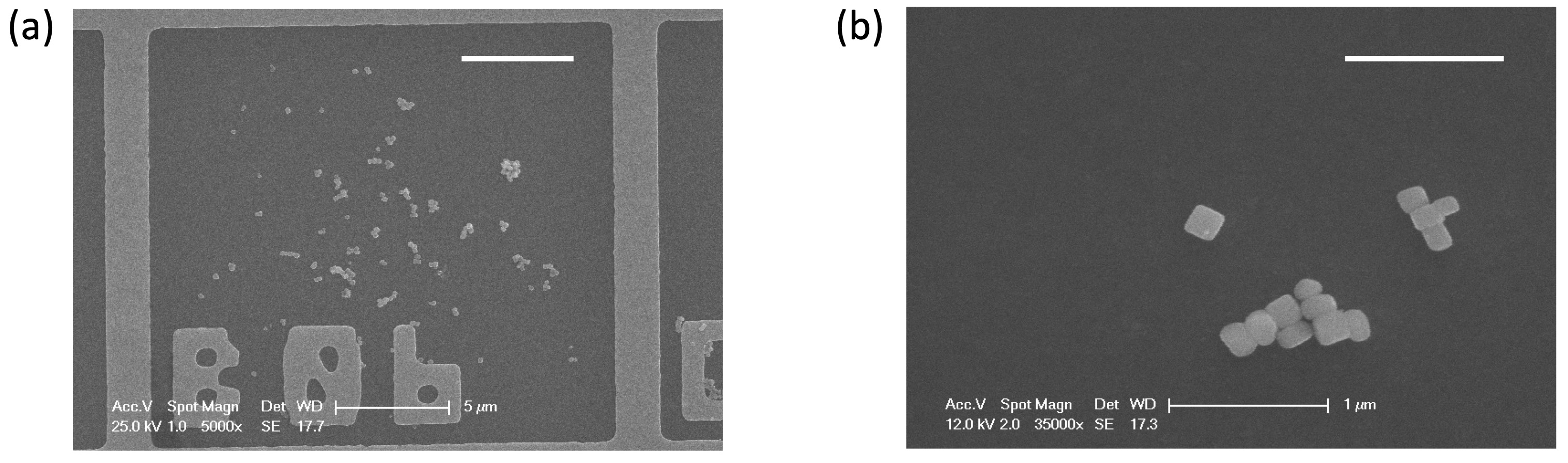
Quasi-cubic shaped barium titanate nanocrystals were synthesized using the solvothermal method described in Bogicevic et al. 19 (Materials and Methods). Supporting Information Figure S1a shows a large field-of-view scanning electron microscopy image of the as-produced powder, confirming the overall quasi-cubic shape. We first did a structural analysis of this powder, from which we then prepared the dilute suspension for PFM studies of single nanocrystals.
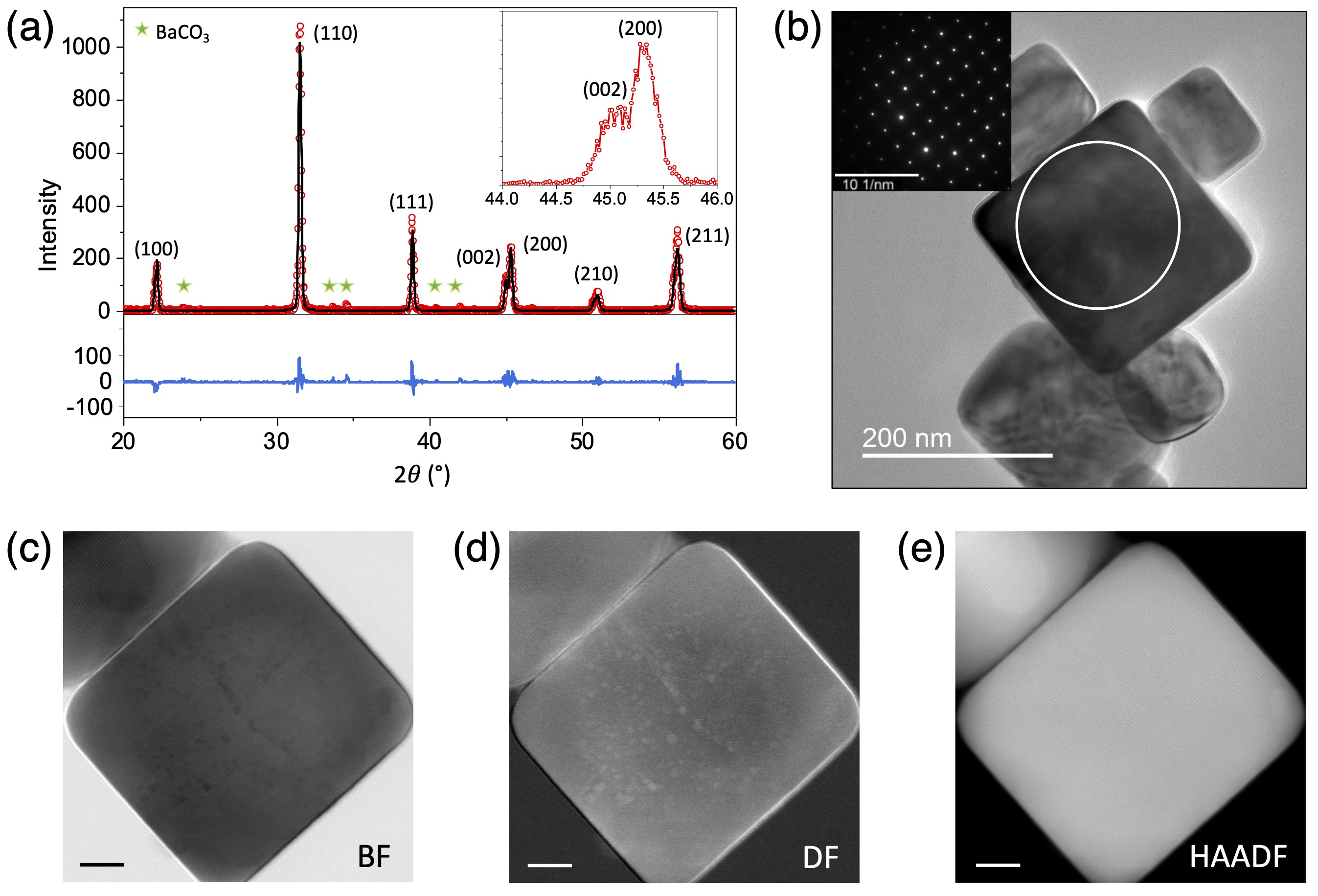
Figure 1a displays the powder X-ray diffractogram at the temperature of 293 K showing the characteristic peak splitting of tetragonal phase at twice the diffraction angle 45∘, corresponding to the Miller indexes and , while a purely cubic phase would have a single peak associated to . Rietveld refinement of the diffractogram (Materials and Methods) reveals a well-known tetragonal structure (space group symmetry P4mm) for BTO at room temperature (293 K), with Å and Å, leading to a lattice parameter ratio . However, compared to bulk BTO for which 34, the ratio measured in our NC is significantly smaller by 0.3% and closer to one, indicating that its lattice is slightly less tetragonal and more cubic than the bulk one, in agreement with other reports on BTO nanocrystals 35, 36. We also used transmission electron microscopy (TEM, Materials and Methods) to investigate the crystalline structure at the single particle level. Figure 1b shows a TEM image of a small aggregate accompanied with the diffraction pattern of the selected area on the central nanocrystal. The regular pattern obtained is consistent with the monocrystalline nature of the selected NC.
The reduced tetragonality that we observed in BTO nanocrystals compared with the bulk was reported in several studies and was attributed to different sources. Firstly, one study evidenced by high-resolution scanning TEM (HR-STEM) the presence of a thin shell of cubic symmetry at BTO NC surface 37. This observation was further supported by indirect measurements and models 36. We examined our BTO NC edge with HR-STEM (see Figure S2) but could not detect a layer of different symmetry. Secondly, we estimated to 0.19% the inhomogeneous strain from Figure 1a diffractogram using Williamson-Hall method with a Cauchy peak profile 38 (see Figure S1b), which is smaller than the value of 0.26% recently reported 39, but not negligible. This strain is probably due to hydroxyl groups coming from the barium precursor and remaining inside the nanocrystals as point structural defects. The latter would migrate to the surface only at temperatures much higher than those used during solvothermal synthesis. Other sources of strain are small square-shape pores that we observed in bright-field (Figure 1c) and dark-field HR-STEM (Figure 1d) of one nanocrystal, but not in high-angle annular dark-field which rather shows chemical contrast. In some particles with rounder morphology we even observed much larger pores (see Figure S2c,d). We reported such pores in a previous study on the same sample 19, and showed evidences that they result from the merging and restructuration, upon temperature increase above 200∘C, of nanotori, which are the primary structure formed at low temperature.
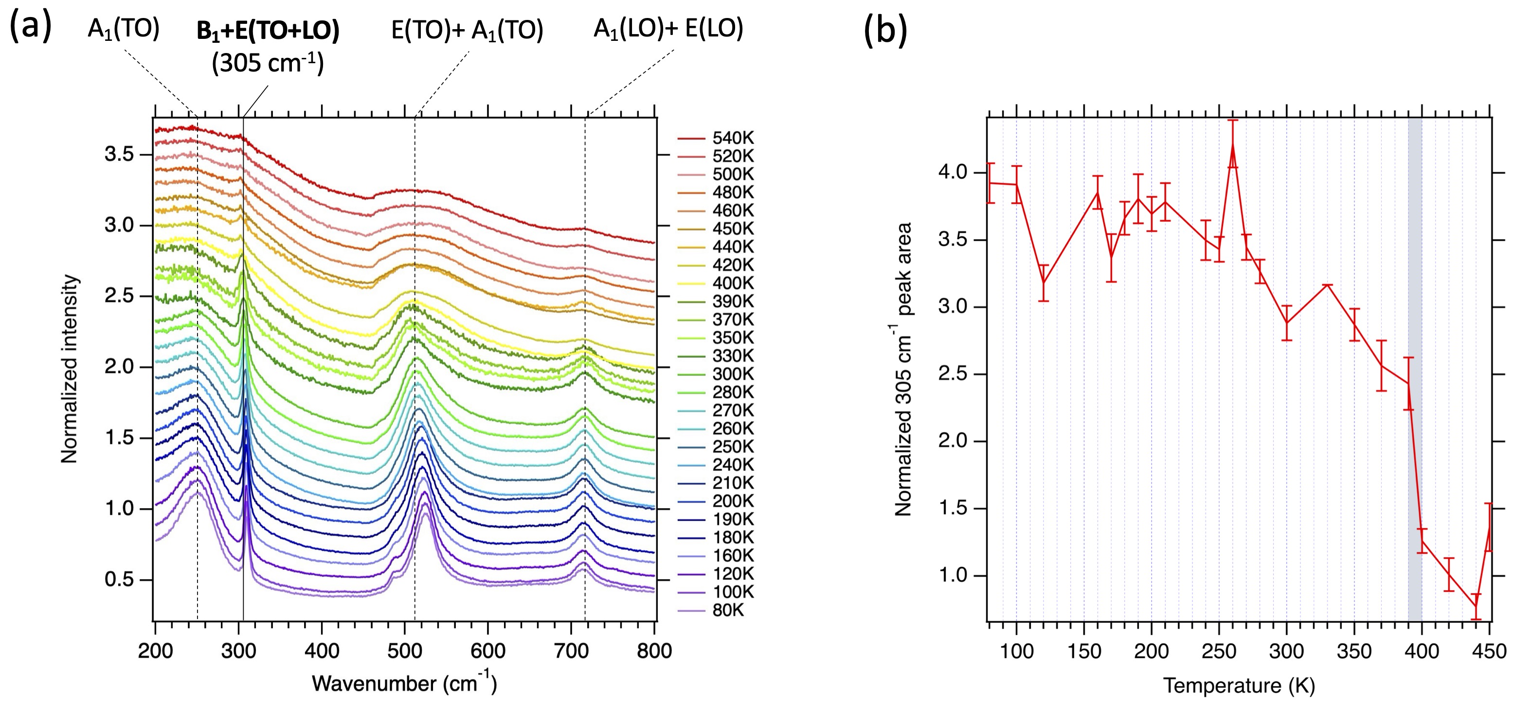
As these defects may impact the ferroelectric properties, we further conducted Raman spectroscopy on BTO powder, at temperatures varying between 80 K and 540 K. In the centro-symmetrical paraelectric cubic phase, BTO is Raman inactive, contrary to the tetragonal phase, which symmetry leads to height Raman optical-phonon active modes40. We monitored the area variation of the narrowest active Raman peak (305 cm-1 wavenumber, at 300 K) with temperature (see Figure S3a), as in Begg et al. 41 and observed a marked decrease at K (Figure S3b) in agreement with the commonly accepted BTO Curie temperature of 120∘C. This observation indicates that, despite a reduced tetragonality compared with the bulk, the BTO NC we synthesized keeps the hallmark of the bulk BTO ferroelectric phase transition. Our objective was then to examine the ferroelectric domain texture of single BTO nanocrystals, and to this aim we performed vector piezoresponse force microscopy 42.
2.2 Piezoresponse displacement measurements
PFM allows nondestructive imaging and control of ferroelectric domains at the nanoscale via bias-induced converse piezoelectric effect mechanical deformations. It has gained interest in helping the development of new nanoferroics 43, 44. The basic principles of PFM are recalled in Supporting Information Text S1 and for example in ref 45. PFM is a near-field microscopy operating in contact mode, which makes the study of individual nanocrystals challenging, as they must be firmly immobilized on a conductive substrate, while having their upper surface directly exposed to the conductive tip.
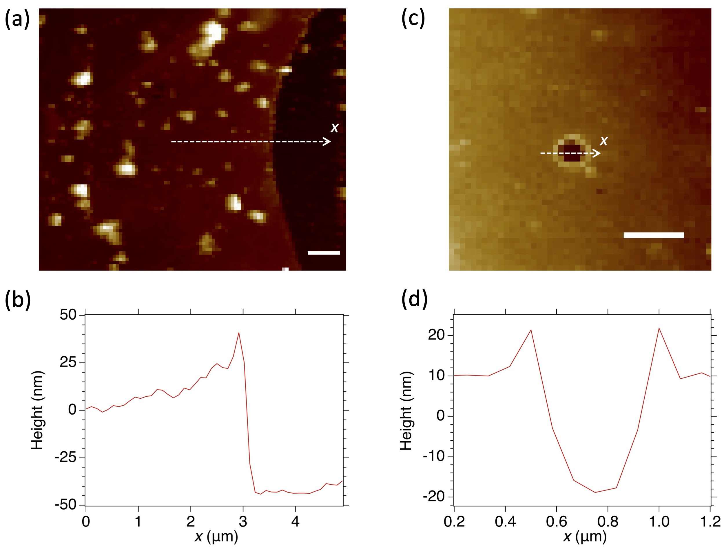
For such a study we prepared a sample with isolated NC attached to a conductive substrate made of indium tin oxide (ITO)-coated coverglass, with a marking grid on top of the coating, to facilitate the correlation between scanning electron microscopy prelocalization of isolated NC and their subsequent study by PFM. The ITO-coated coverglass with the grid is first covered with a thin layer of a conductive polymer (PEDOT:PSS), on top of which a dilute aqueous suspension of the NC is spincoated (Materials and Methods), as displayed on Figure 2a. We optimized the various parameters to achieve a polymer thickness in the range of 40-50 nm (see Figure S4a). Thanks to a good wettability of BaTiO3 by water 46, the concave meniscus (visible on Figure S4b) forming on the edges of the nanoparticles drags them down by surface tension, and after drying the polymer layer in an oven, about two-thirds of the particle height emerges and can be directly contacted by the PFM conductive tip.
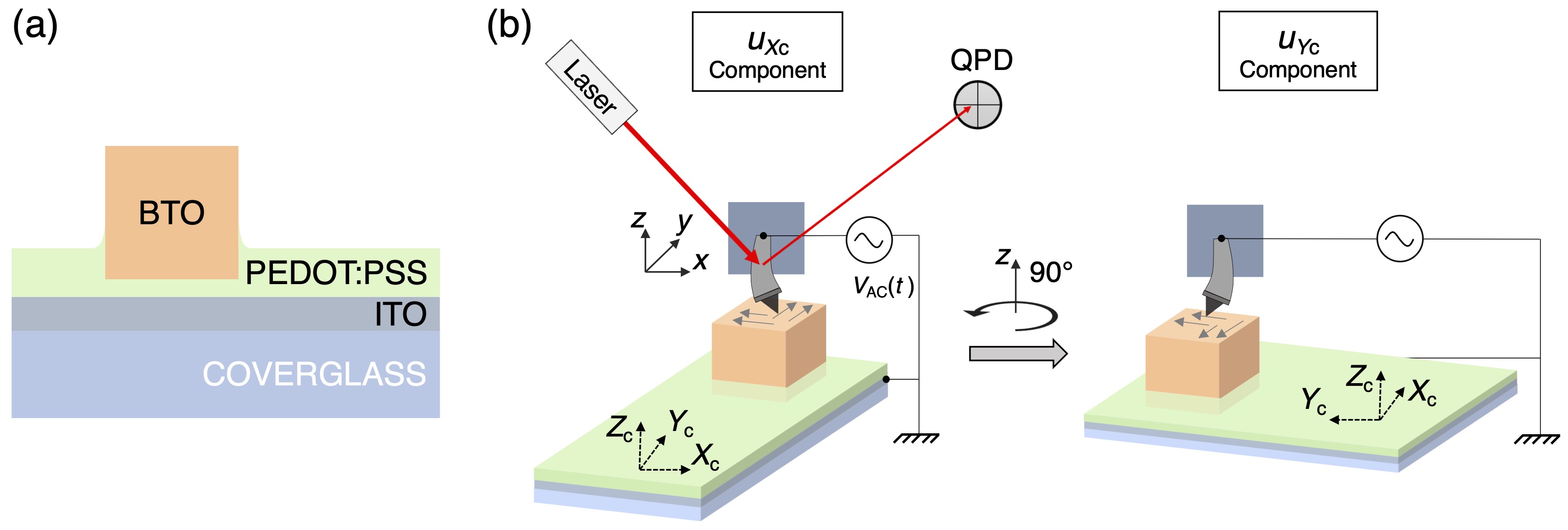
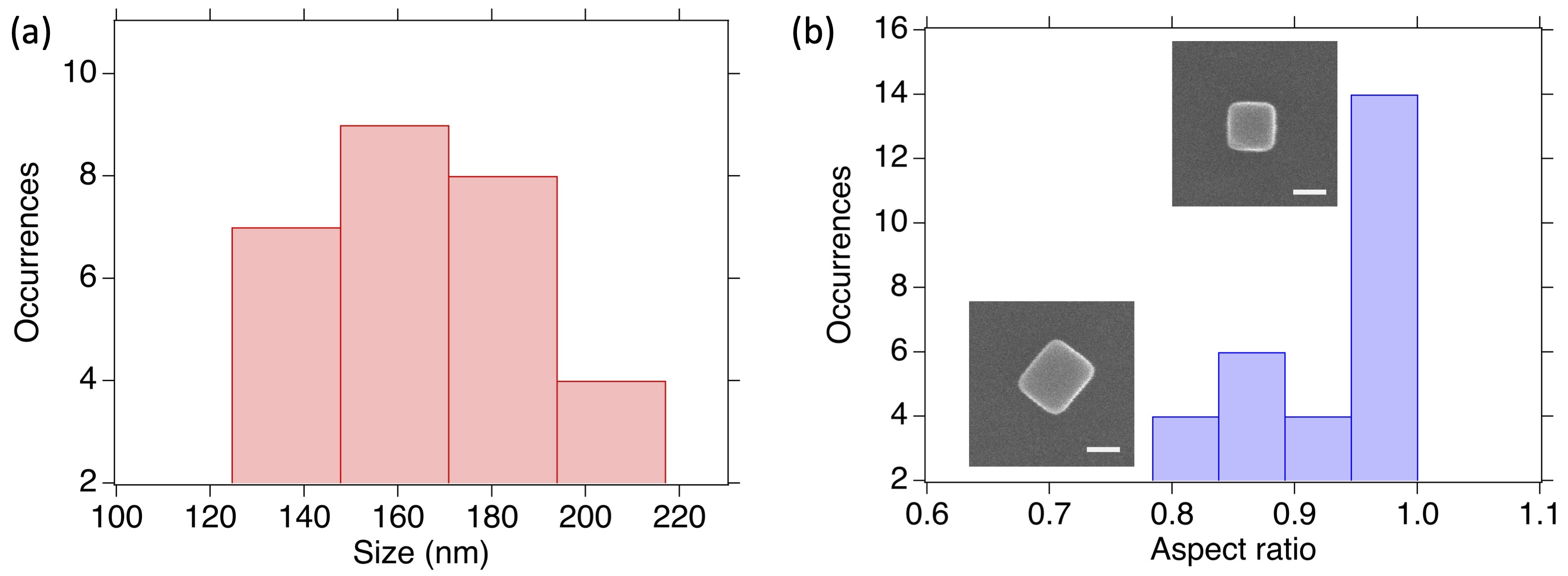
Figure S5a shows a typical low magnification SEM image of the sample with an apparent cell of the numbered grid. To conduct the PFM study, we first selected and located isolated NC, like the one at the center of Figure S5b, and characterized their size distribution, that fell in the range of 120-210 nm, as shown on Figure S6a. Moreover, Figure S6b indicates that about 65% of these NC have an planar aspect ratio larger than 0.95 in the sample plane, which is a good indication of close to perfect cubic shape.
PFM measurements were conducted according to the experimental configuration presented in Figure 2b. We first took care of minimizing artifacts that could stem from electrostatic charge accumulation 47. We evidenced such parasitic effects when using conventional deflection laser spot setting at the cantilever tip. These effects include the observation on the conductive and nonferroelectric surface of the ITO of an apparent contact resonance of the cantilever (see Figure S7a), an hysteresis loop (Figure S7b), and charge accumulation in freshly “written” regions (Figure S8a,b). We were able to strongly reduce these non-electromechanical artifacts by implementing the recently published electrostatic blind spot (ESBS) settings 47 as detailed in the Supporting Information Data S2.2 and shown on Figure S7c,d and Figure S8c-f.
Once these parasitic effects were minimized, we could more reliably map the lateral PFM two-dimensional displacement field (LPFM) of the top surface of immobilized NC. As the PFM cantilever scans only along the direction of the laboratory frame, the sample must be rotated by 90∘ around the vertical laboratory axis, as shown on Figure 2b, to acquire the LPFM component after the one, being a frame of reference attached to the NC of interest.
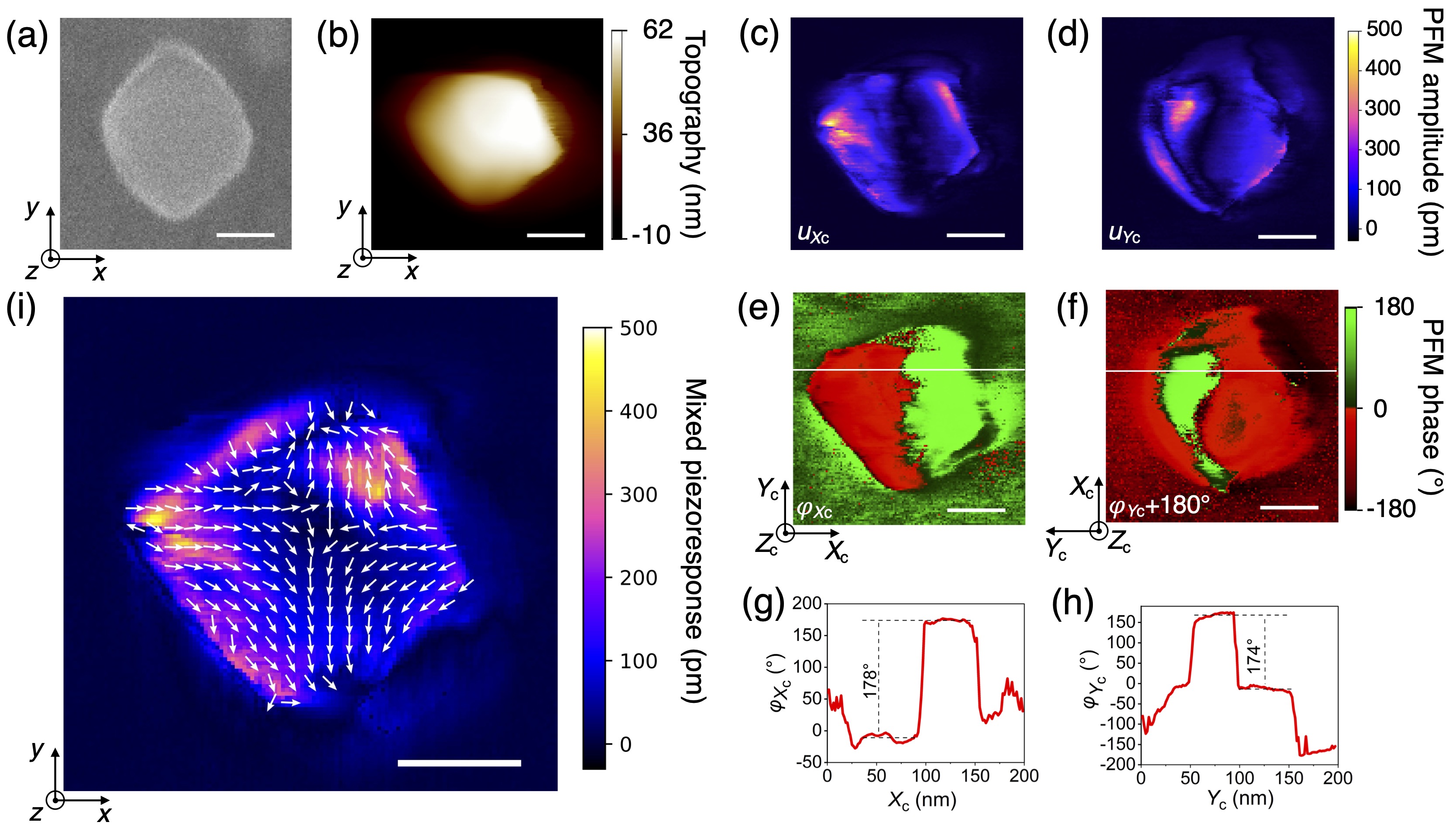
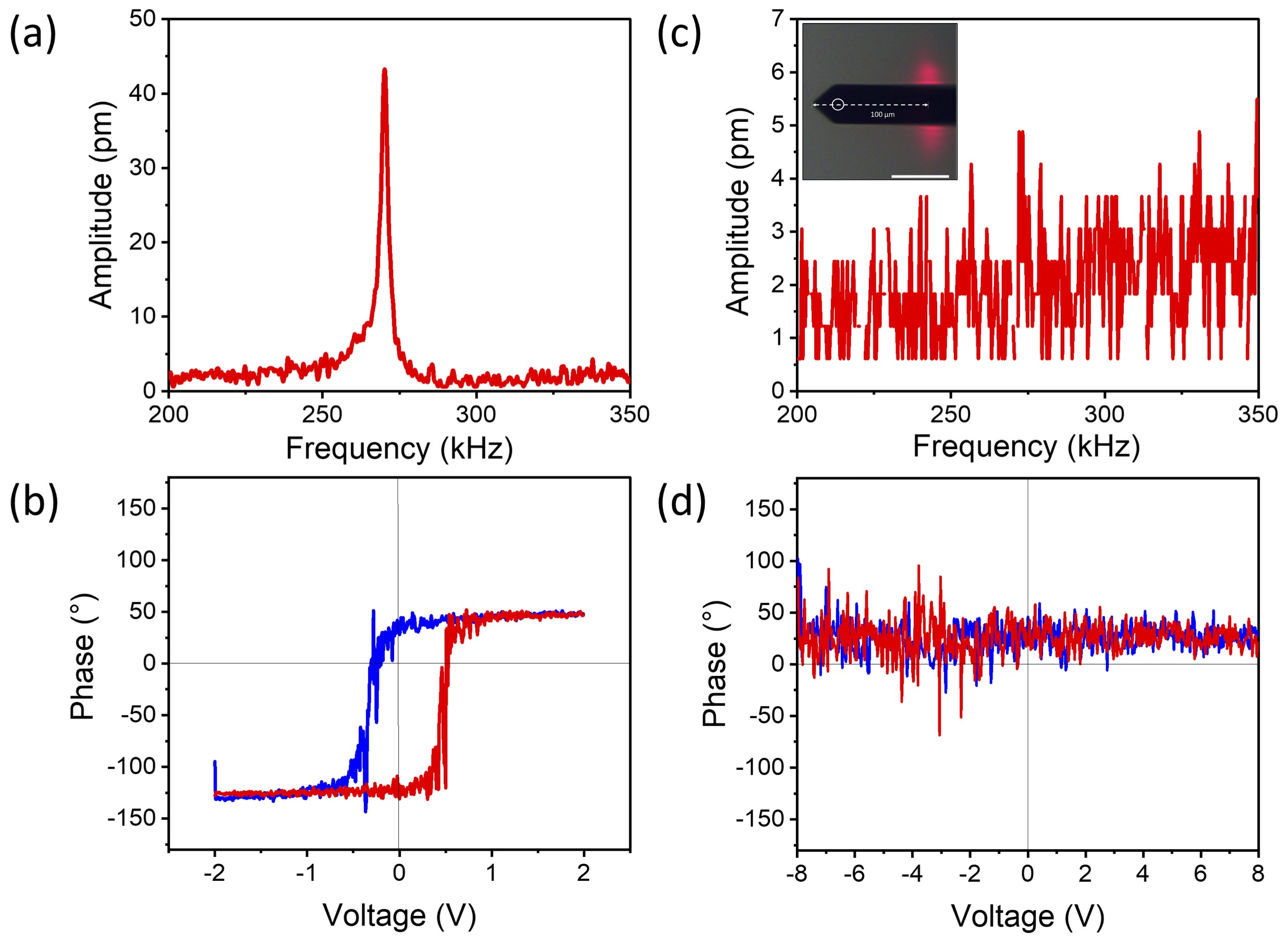
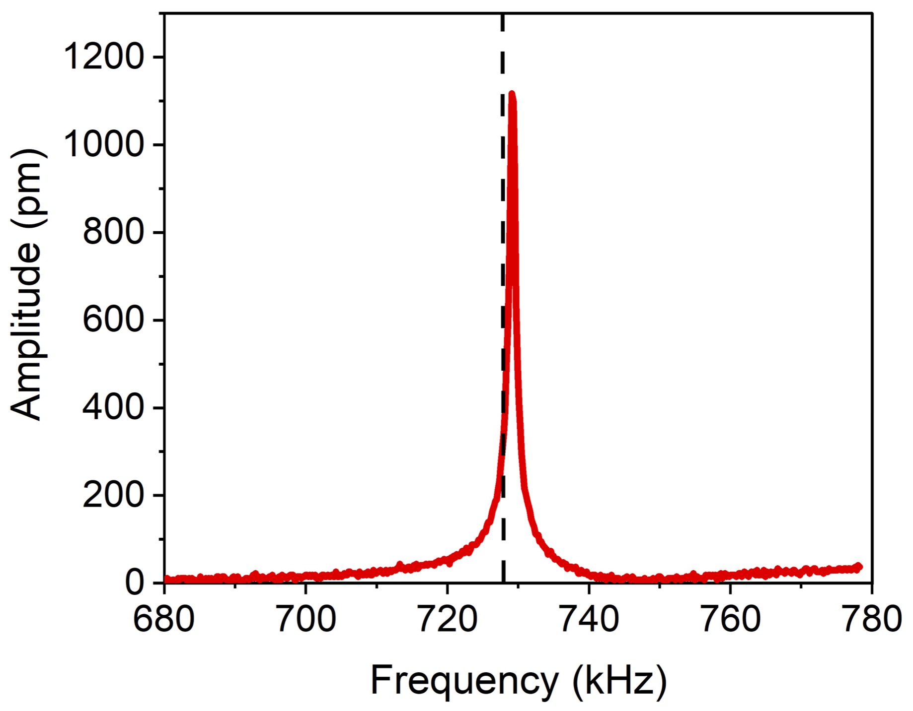
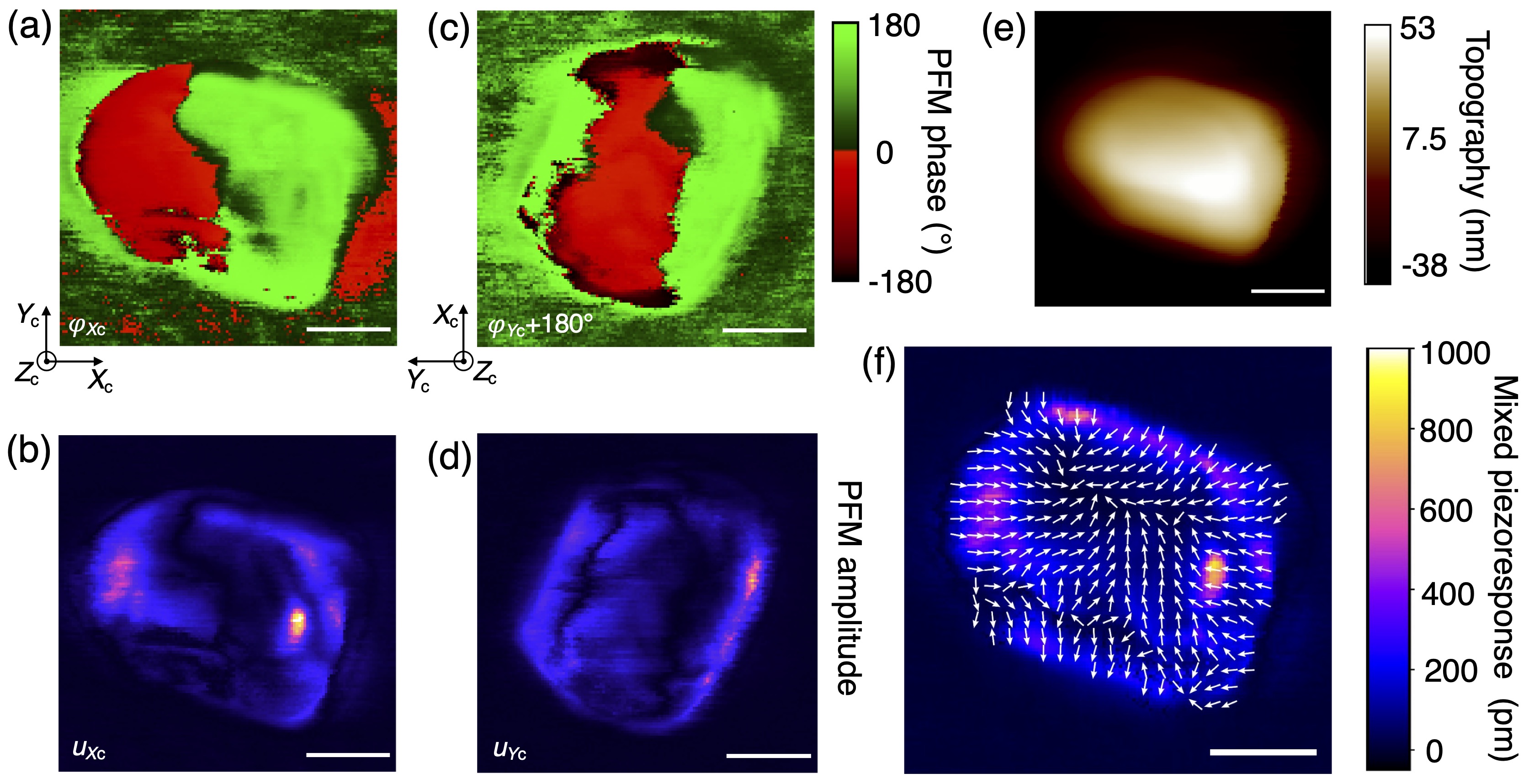
We implemented this procedure to map the LPFM of four nanocrystals, setting the voltage modulation amplitude applied to the tip at V for all of them. Figure S9 shows a typical cantilever contact resonance curve, used to set the driving frequency close to its maximum. Figure 3 exemplifies LPFM measurements in one of the four NC, whose lateral dimensions measured using SEM (Figure 3a) are . The height of the portion of the NC emerging from the PEDOT:PSS layer, as measured by AFM, is nm (Figure 3b). Assuming a cubic shape, the depth of penetration of the particle in the polymer layer is then nm, which is consistent with Figure S4a thickness estimate.
Figure 3c-h then display LPFM measurements carried out on this NC, for which the electric field applied by the tip (along the laboratory axis) has an amplitude kV/cm across the supposedly 125 nm-sized particle. Figure 3c shows a map of , which is the amplitude of the voltage-induced local lateral deformation along the direction. Figure 3e shows the map of the phase difference between applied to the tip and the NC piezoresponse along the direction. To access LPFM measurement along the direction, the sample was rotated counterclockwise by ∘, around the laboratory axis. Figure 3d and Figure 3f show the amplitude and phase maps respectively, along the -direction. Note that the phase actually measured in the rotated-sample orientation is ∘ to account for the fact that the axis, after rotation, points in the opposite direction of the original axis. We observed a small instrumental phase offset, ∘, for the in-phase piezoresponse (refer to Materials and Methods for its determination), which we arbitrarily chose to be the phase of the in-phase domain (with a positive component). The cross-sections of Figure 3e,f evidence a phase difference of between the red and green regions, revealing the presence of in-plane electric polarization domains with opposite orientations along the scanning direction.
We finally inferred the mixed lateral piezoresponse displacement field components, defined as and , displayed in Figure 3i. We observe that the displacement directions close to the nanocrystal edges are either parallel or orthogonal to these edges, and that these orientations propagate from the surface to the center.
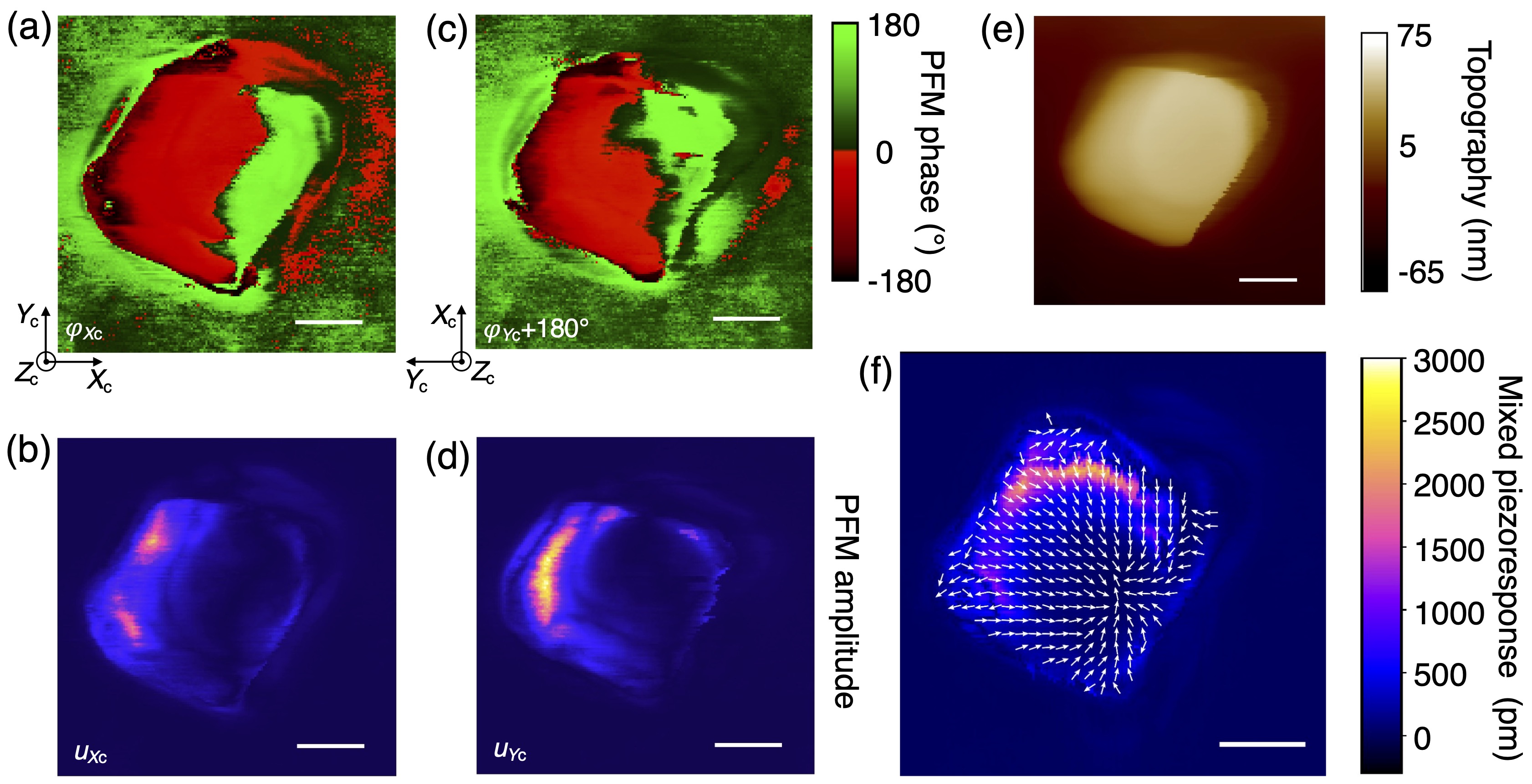
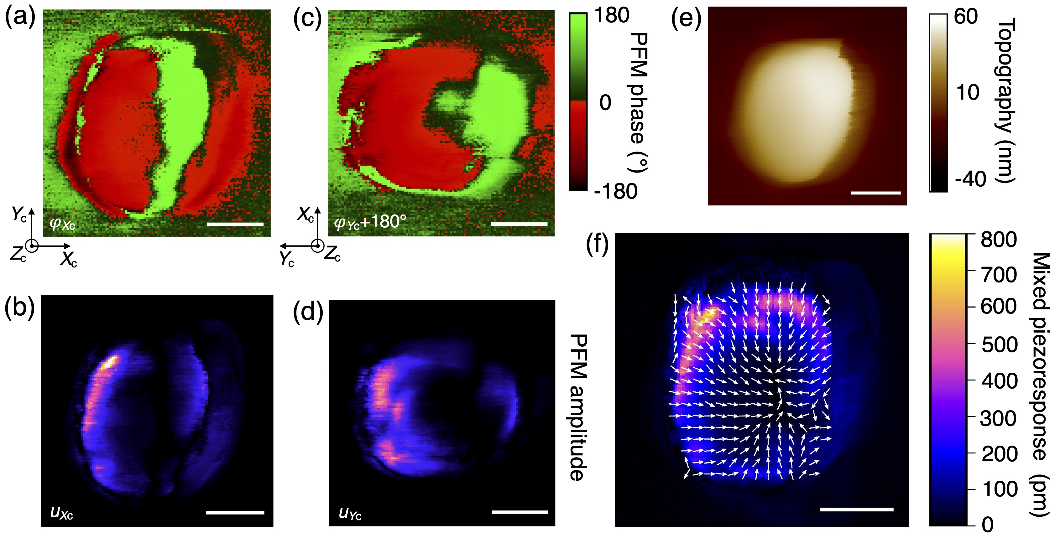
The same behavior was observed for the lateral PFM applied to the three other nanocrystals investigated (see Figures S10 to S12.) The measured lateral responses display non-homogeneous converging deformation fields that reflect complex underlying ferroelectric textures, and that we further investigated by simulations, as discussed later. Note that similar converging deformation fields were reported in single bismuth iron oxide dots of cylindrical shape, nanostructured as an array in a thin layer 14.
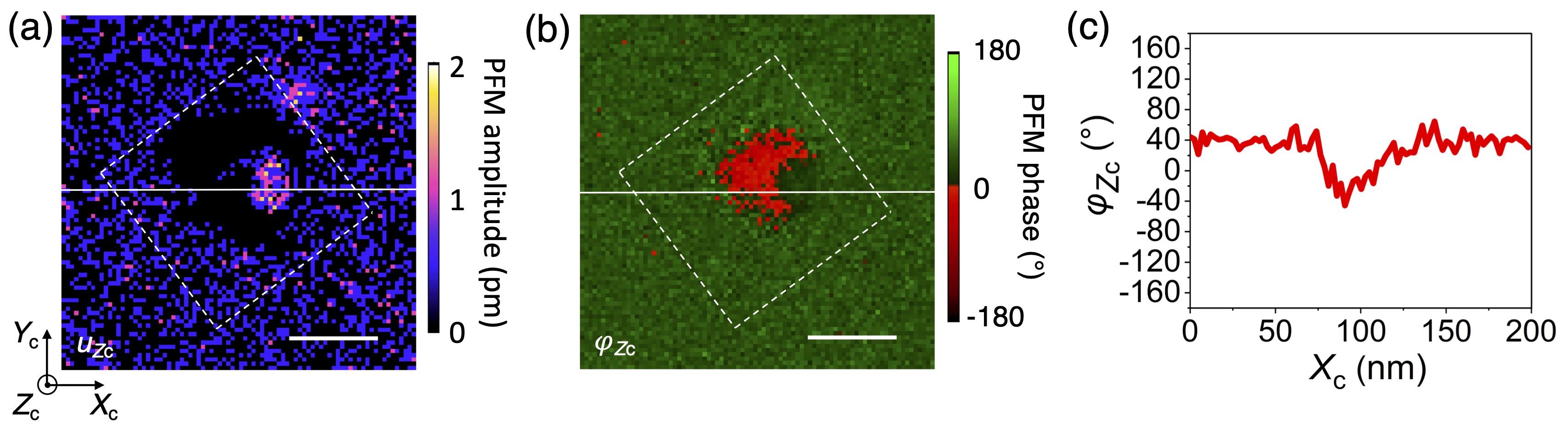
We also measured the vertical piezoresponse (VPFM) that is shown in Figure 4, and detected no significant vertical piezoresponse amplitude compared to the lateral one as (Figure 4a). We observe a phase difference of ∘ relative to the surrounding, in the exact same region where there is no displacement amplitude at all. We therefore suspect that this phase value has no physical meaning.
In order to interpret these PFM data, we carried out ferroelectric phase field simulations, first without any applied external electric field, to get the equilibrium ferroelectric domain distribution, and then in condition of PFM measurement, with an external applied electric field which amplitude is of the order of magnitude of the one used in the experiment.
2.3 Phase field simulations
We considered a cubic-shape BTO nanocrystal of 100 nm size, embedded in air and used the FERRET module 15 of the Multiphysics Object Oriented Simulation Environment (MOOSE), an open-source software maintained by Idaho National Laboratory 48. FERRET is a finite element implementation of a ferroelectric phase field model, which we utilise here to capture the polar and elastic equilibrium state of BTO nanocrystals, as well as their response to static electric fields. In the experiment, one facet of the particle is in contact with a conductive medium. However, as shown in Prosandeev and Bellaiche 49, asymmetric screening with a metal electrode does not destroy the domain structure in ferroelectric thin films, and the simulations conducted probably extend to the experimental case of the bottom facet surface attached to a conductive layer with the rest of the nanocube exposed to air.
Equilibrium domain structure.
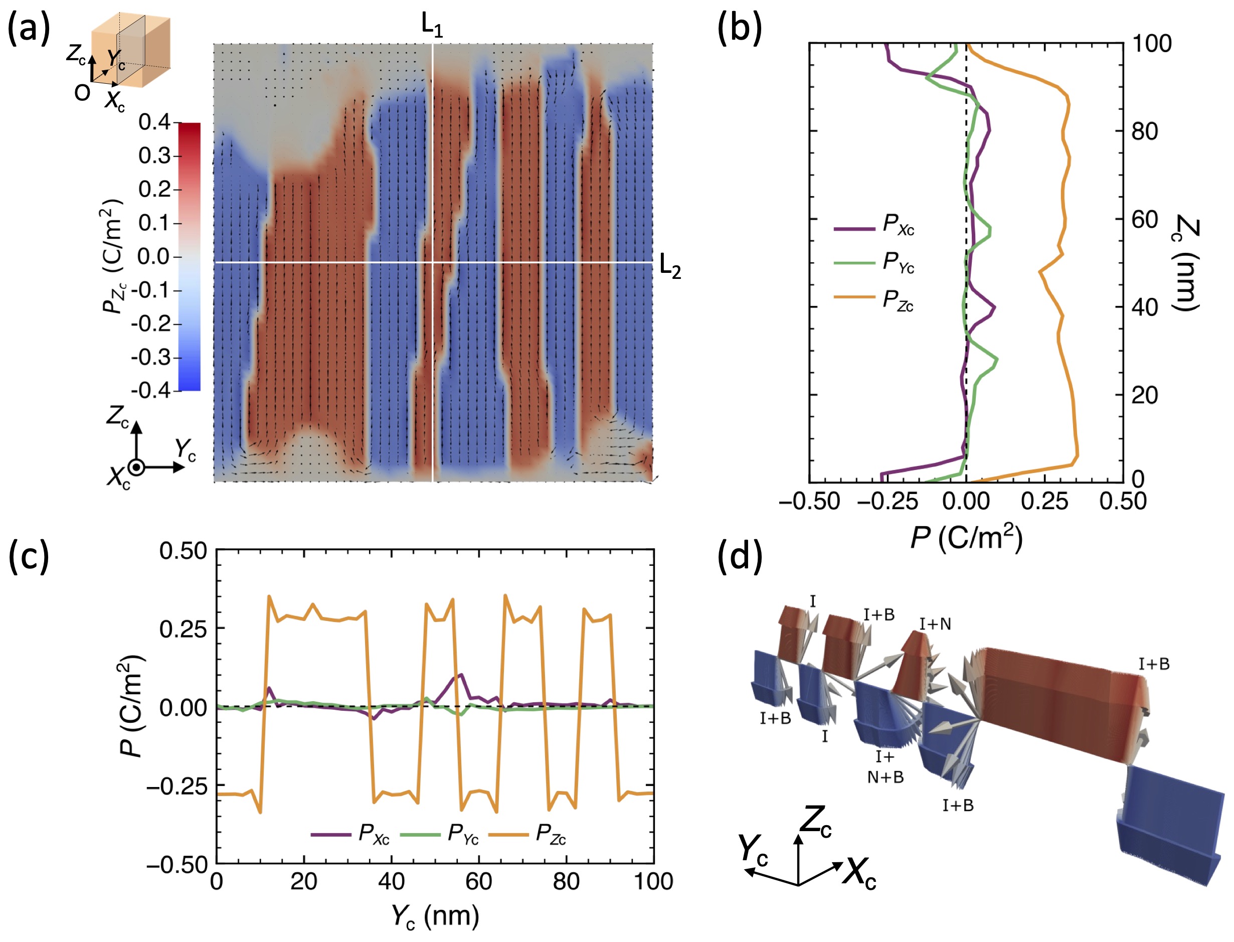
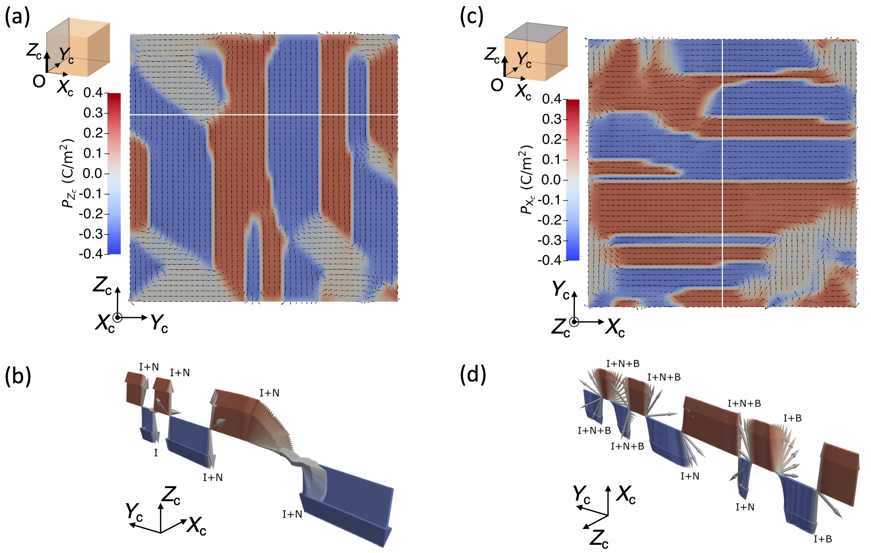
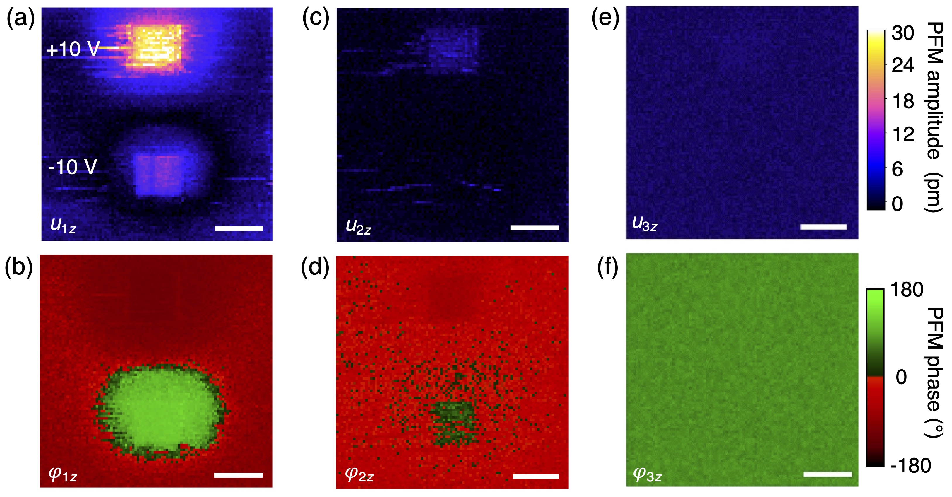
We first determined the equilibrium polarization and displacement fields, and by minimising the energy of a BTO nanocube with random and small initial polarization and mechanical displacement field components. Figure 5a shows that minimization of the free energy of the system leads to a multidomain structure consisting of domains polarized upward and downward along the (O) axis, which we now refer to as the polar axis [001]. We estimate that the core of the BTO NC made of upward and downward tetragonal domains along (O) represents 60% of the fraction of the volume of the NC. From the polarization profiles along lines L1 and L2 (Figure 5b,c), we inferred a polarization component amplitude C/m2 in these up and down domains, which is consistent with what has been measured 50 or calculated 51, 52 in the tetragonal ferroelectric phase of barium titanate.
Looking at the domain walls separating up and down domains in Figure 5c polarization profile, we observe that they are mostly of the Ising-type, i.e. the transition is accomplished by modulating the component. We do see, however, that some walls retain partial Bloch characteristics (rotation of the polarization in planes parallel to the domain wall, i.e. showing non-vanishing component, for example at 11, 35, 55 and 90 nm) or Néel characteristics (rotation of the polarization in a plane orthogonal to the domain wall, i.e. with non-zero , for example at 45 and 55 nm), as schematized on the polarization profile line L2 in Figure 5d.
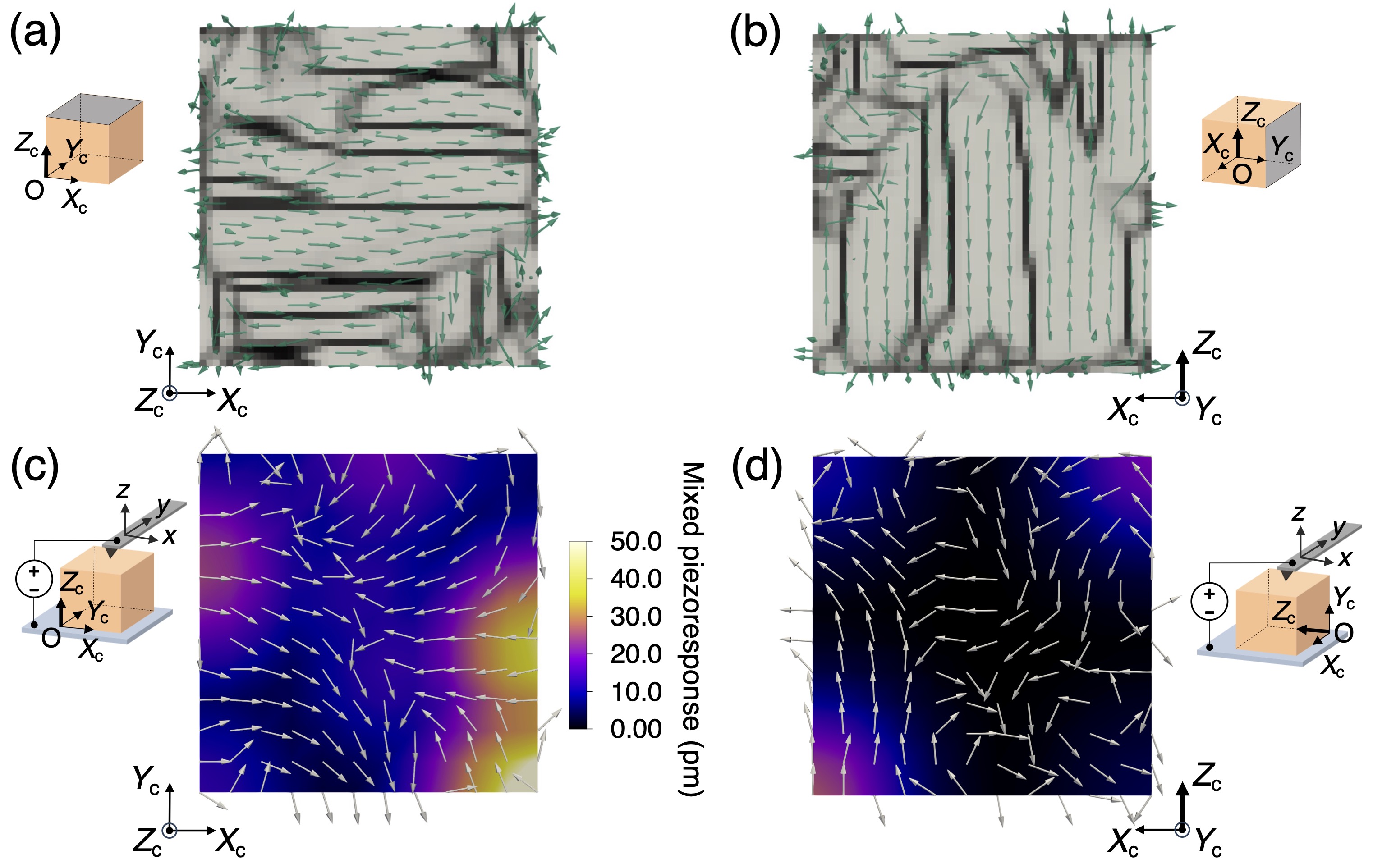
Note that, in surface planes along the polar axis like nm, the polarization aligns up and down along (O) like in the bulk (see Figure S13a) and the domain walls are also of Ising type with partial Néel characteristics (Figure S13b).
Let us now focus our attention on the facets of the NC perpendicular to the polar axis, and nm. Interestingly, the component of the polarization field vanishes near the surface of these facets (see Figure 5a,b). Instead, the polarization lies in the plane of these facets, as shown in Figure 6a and Figure S13c (facet nm), with mostly tetragonal domains polarized along the (O) direction (representing about 16% of the total NC volume), as well as a lower number of domains polarized along the (O) direction (about 7% of the NC volume). These surface domains extend at an average depth of 8 nm (see Figure 5a,b) from the surface of the and nm facets, and they also display Ising domain walls with Bloch and/or Néel characteristics (Figure S13d) like in the core of the nanocrystal (Figure 5d).
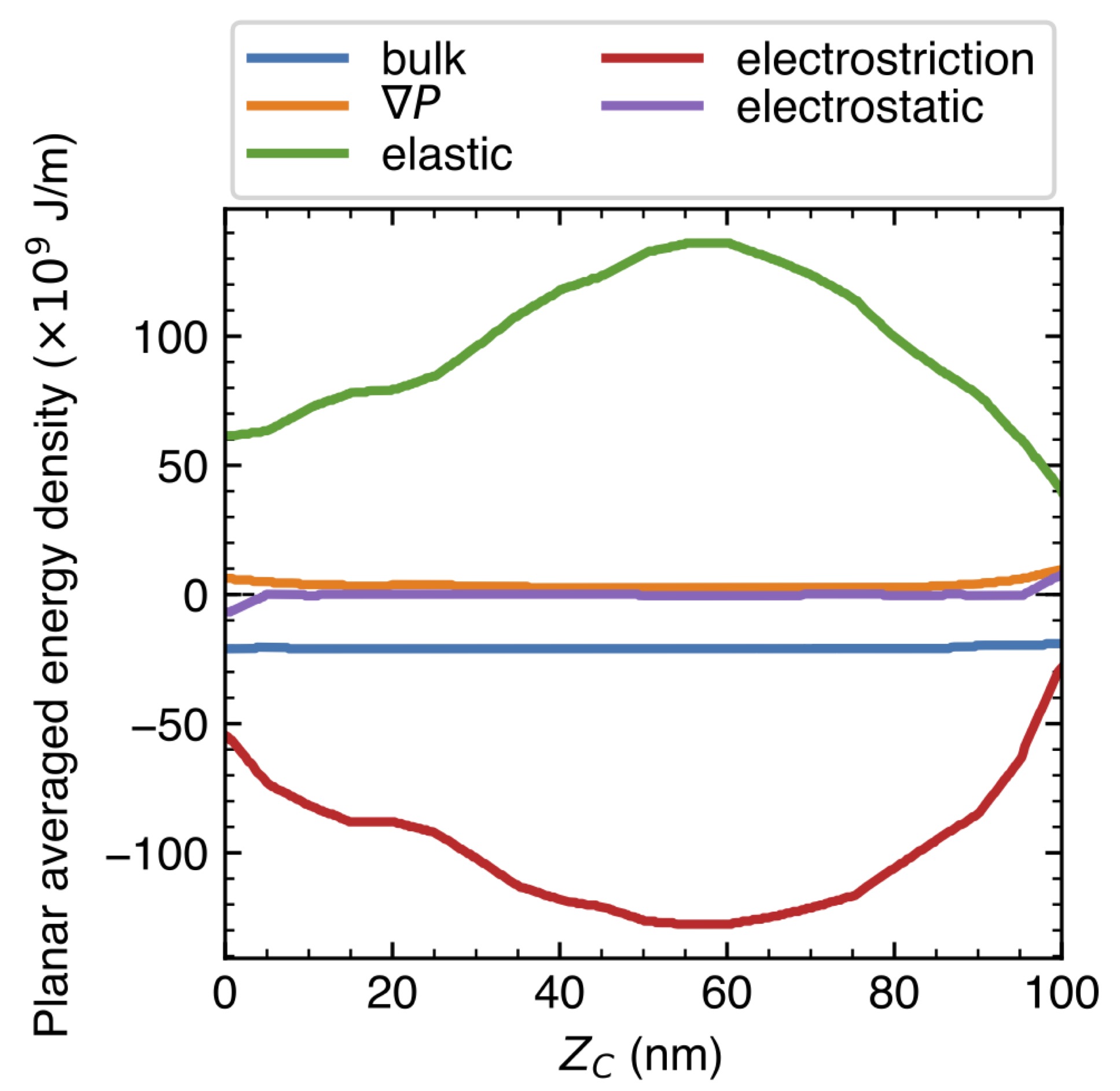
Rotation of the polarization from (O) direction to either (O) or (O) one allows the system to prevent a strong electrostatic depolarizing field. Indeed, the averaged planar electrostatic energy density in the equilibrium structure is mostly zero (see Figure S14). Depolarizing fields, which appear when polarization-induced bound charges are imperfectly screened at an interface, are well known in ferroelectric thin films 53, 54. They are responsible for the emergence of flux closure patterns 55, 49 in which the polarization field rotates from the out-of-plane direction to lie in the plane of the thin film surface, similarly to our NCs, as well as for the appearance of more exotic polar textures such as polar vortices 56, which we do not observe here. Rotation of polarization on surfaces normal to (O) thus allows the NC to sustain uniformly polarized domains, at the cost of an increase in electromechanical energy near the surfaces. Nonetheless, this is counteracted by the release of elastic energy by the domain walls near the surface (see Figure S14).
Lateral piezoresponse force response simulation.
Starting from the equilibrium solution described in the previous paragraph, we now apply a finite electric field to simulate PFM experimental conditions. The BTO nanocrystal is then relaxed under this applied electric field, leading to new equilibrium values of the polarization and mechanical displacement fields.
Let us first consider the case when an electric field of amplitude kV/cm is applied along the polar axis (O) direction of the BTO nanocrystal. The difference between the zero-field and finite-field mechanical displacement fields gives us an estimate of the electromechanical response of the nanocube. We show, in Figure 6c, the resulting electric-field-induced mixed piezoresponse in the “top” facet perpendicular to the polar axis ( nm facet). We observe qualitatively similar LPFM data of Figure 3i, Figure S10f, S11f and S12f, with local regions of pronounced in-plane displacement at the corners and edges of the facet. We also observe a low to vanishing in-plane piezoelectric displacement in the inner region of the facet, as evidenced experimentally as well.
To investigate the other experimental configuration of the nanocube having its polar axis (O) lying in the substrate plane, parallel to the laboratory plane , we also simulated the application of an electric field along the (O) axis using the same equilibrium condition as depicted in Figure 5. The resulting mixed piezoresponse simulation, presented on Figure 6d, exhibits lower (by one order of magnitude in the center of the facet and by a factor of 2 to 5 at the edges) and contrast than the simulation for the field applied along (O). It is well known that the presence of 90∘ twin domain walls contribute to the piezoelectric response of BTO 57, 58, 59 and can strongly enhance it. Indeed, contrary to the (O) facet, the (O) possesses multiple 90∘ domain walls, at a distance of about 8 nm from the surface, due to a 90∘ rotation of the polarization from a axis aligned orientation (as displayed for nm facet in Figure S13a) to an in- plane lying one. This may explain the larger simulated in-plane electromechanical response when the electric field is applied along the axis (Figure 6c).
We note that the magnitude of the maximum in-plane displacement observed experimentally (Figure 3i) is one order of magnitude larger than that obtained from the simulation (Figure 6b). Apart from the fact that we did not calibrate PFM lateral displacement, two other factors may contribute to this difference. First, in the experiment the amplitude of the electric field effectively applied to the nanocrystal is not known precisely because the PFM geometry results in a pronounced inhomogeneous radial distribution with a larger field valued compared to the one of the uniform field applied in the simulations (considering the same applied voltage). Second, in the simulations the applied electric field is static, while the PFM tip applies an AC voltage oscillating at a frequency set close to the electromechanical resonance, hence enhancing the displacement.
3 Conclusion
It is now well established theoretically and experimentally, that ferroelectric materials at the nanoscale exhibit exotic polarization texture, leading to unconventional properties. The case of 0-dimension ferroelectric nanocrystals, in particular isolated ones, has been far less studied experimentally, despite the opportunity it offers to bring novel properties due to their large surface to volume ratio. In this work we considered isolated barium titanate nanocrystals immobilized on a conductive surface and exposed to air. Using a solvothermal approach 19 we were able to synthesize NC of a well-defined cubic shape and 160 nm average size, that conserve the tetragonal structure of BTO at room temperature (293 K), are individual monocrystallites (as observed by TEM) and exhibit the expected transition to a cubic symmetry phase above 120∘C, the known Curie temperature of the ferro- to para-electric phases. We then investigated, at room temperature, the inverse piezoelectric properties of such pristine individual NC by piezoresponse force microscopy. To this end, we developed a methodology that combines the firm attachment of the NC to the substrate with a conductive polymer and the fine adjustment of the deflection laser in a position along the PFM cantilever that strongly reduces electrostatic artifacts 47. This strategy allowed repeated measurements on the same particle without risk of being dragged with the PFM tip and provided a high confidence in the crystal deformation fields recorded. We observed that none of the NC showed any vertical PFM displacement, while all showed lateral displacements. We reconstructed mixed piezoresponse fields from the 2D LPFM recording of the same NC for two orthogonal orientations relative to the cantilever (attached to the laboratory frame). All the NC studied showed an inhomogeneous LPFM field of larger amplitude along the edges, a minimum at the center with deformations that tend to be oriented towards this lower-amplitude central region.
To check whether these observations were consistent with the underlying texture of the volume polarization, we conducted phase field simulations 15, 17. These simulations revealed that in the equilibrium state at the temperature of 293 K, a polar axis (O) with up and down 180∘ domains emerges in the core, accompanied with 90∘ domains on the two surfaces normal to this axis in a layer of an average thickness of 8 nm. In this layer, there is a dominant polarization orientation in the plane with mostly 180∘ and a few 90∘ domains (on the edges). Hence, the phase field simulations predict that none of the cube facets possess an out-of-plane polarization component, which is consistent with the PFM observations. We investigated the nature of the domain walls, as predicted by the simulation, and found that they are mostly of the Ising type with Bloch and/or Néel characteristics. We then simulated the LPFM field by calculating the difference between the equilibrium position of atomic displacement in the zero electric field and in the presence of an amplitude-similar electric field as applied during the PFM measurement. The resulting simulated LPFM 2D-maps strongly resemble the experimental ones, with maximum displacement amplitudes along the edges and in the corners, and displacement vectors mostly following the gradient of amplitude.
The results of our study challenge the interpretation of second harmonic generation (SHG) by nm-sized BTO nanocrystals, implicitly considered composed of a single static polarization domain in all reported studies 60, eventually bearing a cubic symmetry shell61. As the 180∘ domains dominate the core and surface of the NC in a balanced up- and down-fraction, we expect that it yields a destructively interfering SHG field, leaving open the origin of the observed nonlinear contrast. Correlative SHG and PFM investigations may contribute to resolve this issue. Finally, ferroelectric matrices doped with luminescent reporting ionic species have also been considered for sensing applications, including temperature 62 and electric fields 63, 64. The complex polarization structure of BTO nanocrystals that we revealed in our study should be considered to design optimal ferroelectric-based nanosensors.
4 Materials and Methods
4.1 Sample preparation
BTO nanocube synthesis and characterization.
Barium titanate nanocrystals were synthesized using the solvothermal method described in Bogicevic et al. 19. Briefly, in a solvent made of volumic proportions of 60% ethanol and 40% deionized water, we mixed, in a nitrogen environment, solid Na2Ti3O7 titanium and soluble Ba(OH)H2O barium precursors. We then heated the mixture at 250∘C in an autoclave under autogeneous pressure for 24 hours. We selected a Ba/Ti atomic ratio of 1.6 as it leads to BTO nanocrystals of mostly cubic shape and relatively homogeneous size, as can be observed on Figure S1a SEM image, in the range of 100-350 nm.
XRD measurement (Figure 1b) was performed at 293 K using the Cu K1 (= 1.5418 Å) and Cu K2 radiations (= 1.5444 Å) of a diffractometer (D2 Phaser from Bruker AXS GmbH, Germany) and collecting data in steps of 0.02∘. We then extracted the structural model with DIFFRAC.EVA (Bruker) software, and performed Rietveld refinement of the structural model using the WinPlotr/FullProf package 65 with peak shape described by a pseudo-Voigt function and background level modelled using a polynomial function. The refined free parameters were background coefficients, scale factor, lattice constants, zero shift, peak profile, and asymmetry parameters.
For single BTO NC experiments, we prepared an aqueous colloidal suspension of BTO NC at the stock concentration of 1 mg/mL.
BTO NC immobilization.
To enable contact mode PFM imaging on individual BTO NC, we immobilize them on a 170 m thick glass coverslip with a conductive 80 nm-thick layer of indium-tin-oxide (ITO) deposited on it. Furthermore, a numbered grid made by gold-deposition and with the smallest cells of 30 m size was deposited on the ITO-coated coverslip. This allows us to address the same individual BTO NC after 90∘ rotation and also with other analytical methods. For immobilization while maintaining electrical contact, we first spin-coated a 40-80 nm thick layer of an aqueous suspension (at 1% weight concentration) of a conductive polymer PEDOT:PSS (Ref. 768618, Sigma Aldrich) onto the marked ITO-coated coverslip. Subsequently, the stock solution of BTO NCs was first diluted by a factor of 50 in water, then spin-coated onto the coated coverslip and the sample was finally annealed at 95∘C for 30 minutes. While the literature suggests annealing PEDOT:PSS at temperatures ranging from 80∘C to 160∘C, we deliberately maintained the annealing temperature below 100∘C to avoid any potential phase transition of BTO, which typically occurs at a Curie temperature of 120∘C.
4.2 PFM measurements
For PFM we used a commercial apparatus (Dimension ICON head system and Nanoscope V controller, Bruker Inc.). The measurements were conducted using SCM-PIT-V2 (Bruker) probes, which have conductive platinum-iridium coated tips with a radius of curvature of 25 nm and a nominal spring constant of 3 N/m. We acquired the piezoresponse phase and amplitude signal while scanning the tip along the laboratory frame axis direction (see Figure 2b), with the cantilever along axis.
Minimization of electrostatic effects.
It is widely recognized that PFM measurements can exhibit artifacts, leading to possible misinterpretations of the data. The signal artifacts are mainly caused by non-electromechanical effects such as electrostatic force that arises due to the electrostatic potential difference between the cantilever and the sample66. This force generates a bending response in the cantilever of the AFM that is not distinguishable from the true PFM signal. The strength of this force is highest near the tip-sample junction and decreases with increasing distance along the cantilever. To address this issue, we employed the concept of electrostatic blind spot position (ESBS) for the laser, as recently introduced by Killgore et al. 47. In ESBS, the laser spot, which is usually placed just above the tip, is positioned along the cantilever where the bending induced by the electrostatic force is minimised, in order to get a piezoresponse amplitude dominated by the electromecanichal contribution. The signal thus obtained will be predominantly dominated by the true PFM signal caused by the bending of the cantilever due to inverse piezoelectric effect. The ESBS position was determined to be at a distance of 0.45 times the length of the cantilever.
PFM measurements were done on single isolated BTO NCs preidentified using scanning electron microscopy (SEM). The lateral PFM phase and amplitude images were taken using a drive voltage of 1.5 V and a drive frequency of 727.856 kHz (near in-plane contact resonance of the cantilever). We used a scan speed of 0.35 Hz and utilized 192 scan lines across a full scan size of 300 nm resulting in 1.56 nm pixel size.
LPFM phase offset estimation.
To estimate , we first selected one domain with the smallest phase values, close to 0, as the reference, and computed a first phase offset as the phase average value within this domain. In parallel, we identified another domain with phase values close to 180∘. Subtracting 180∘ from the phase of this second domain led to a second phase offset. By averaging these offsets, we obtained a final offset value of ∘ for the PFM scan along the (O) direction. The same process was repeated for the PFM scan along the (O) direction, producing an average offset value of ∘. As this offset is attributed to the instrumental response and should be the same for both scans, regardless of particle orientation, we took the average of these two values, resulting in .
Vector lateral PFM mapping.
To build the lateral displacement field of probed-NC facets, we first had to register component map with map, as they were acquired separately. We only considered translations shifts between the two scans, as rotation mismatch could not be assessed with a precision better than the uncertainty on the physical 90∘ sample rotation. The translation vector shift between and components was determined using Fiji-ImageJ software 67, based on the largest overlap of the raw PFM amplitude images. We then represented the mixed displacement amplitude and vector map.
4.3 Piezoresponse simulation
Simulations of an embedded BTO nanoparticle have been performed using FERRET15, a module for simulating multiferroic phenomena in the MOOSE finite element framework48. We consider the equilibrium domain structure and piezoresponse of a stress-free BTO nano-cube (100 nm size) embedded in a dielectric infinite medium (here assumed to be air), by evolving a time-dependent Landau-Ginzburg-Devonshire equation, , with representing the free energy of the system.
The Helmoltz free energy volume density includes several terms, introduced in Hlinka and Marton 51 and which analytical expressions are given in the Supporting Information Text S2:
| (1) |
where is the contribution to the energy stemming from the local polarization field . In a uniaxial ferroelectric, this typically has two degenerate minima and a double-well shape as a function of the polarization value. This is typically the case in BTO and indicates the desire of the system to form a uniformly polarized ferroelectric domain. The term depends on the gradient of the polarization field and tends to oppose variations of the polarization field. The term depends on the derivative of the local atomic displacement field (defined relative to a cubic parent lattice structure) and describes the linear elastic response of the system. The electrostrictive term gathers the electromechanical energy couplings between the polarization field and the displacement field . Finally, represents the energy density caused by internal/external electric fields. As stated earlier, as we consider a stress-free condition, the strain energy term , where is the stress and the strain tensor, resumes at zero. To realize our simulations of ferroelectric domains and displacements on the BTO NC at the ambient temperature of 298 K, we adopted numerical coefficients from ref. 51 for the numerical values of the coefficients involved in each term of energy density. The displacement field is obtained by solving the stress-divergence equation (neglecting gravity) with mechanical boundary conditions without stress at each time step.
The computational domain comprises the BTO nanocrystal, with 100 nm long sides embedded at the center of a dielectric matrix, with 200 nm sides in order to capture the depolarization field around the inclusion. The relative permittivity of the dielectric matrix is set to 1 and the NC is considered stress-free, simulating an open air environment. Dirichlet boundary conditions on (), are applied to ensure that displacement and electrostatic fields disappear far from the particle. Partial clamping and dielectric screening by PEDOT:PSS could lead to a slight alteration of the ground state and the piezoelectric response through modulation of the surface layer thickness and potential Poisson effects which could lead to enhanced out-of-plane mechanical response.
The equilibrium structure at zero applied electric field is obtained by relaxing the system starting from a reasonable approximation of the paraelectric state, realized by initializing random, small component (C/m2) values to the polarization and local displacement fields. Through the gradient flow approach, the system variables are evolved through a dynamic time stepper until a local minimum is reached, defined by a convergence criterion of within of the total energy of the previous time step.
The average thickness of the surface layers are estimated by the ratio of the volume having to the volume of the nanocrystal, multiplied by the nanoparticle size. The obtained averaged thickness of 8 nm correlates well with typical thicknesses which can be estimated from Figure 5b.
Coupling to internal/external electrical fields is accomplished through the Poisson equation, , where is the electric potential, related to the electric field through , and is the surrounding medium relative permittivity, which in our case is air for most of the particle volume, hence . Hence, to mimic PFM experiments, we use the following procedure. First, we start with the zero-field equilibrium structure. We then relax the polarization and local displacement fields by solving the Landau-Ginzburg-Devonshire equation and the stress-divergence equation at each time step, under an applied external electric field of 150 kV/cm, until the new equilibrium is reached. The difference in equilibrium local displacement fields between the configuration with and without applied electric field gives us the electric-field induced displacement in the BTO nanocube, which we report in Figure 6c,d and compare to lateral PFM experiments. Note that to compare with the experimental observations, a Gaussian blur with 20 nm diameter was applied to the local displacement field.
Author contributions
Conceptualization: BD, CFD, CP, and FT; Methodology: AM, KC, KP, CFD, CP and FT; Software: KC and CP; Validation: AM, KC, CFD, CP and FT; Formal analysis: KC and CP; Investigation: AM, AZ, MV, and KC; Resources: CB and FK; Data curation: CB, MV, AM and KC; Writing – Original draft: AM, KC, CP and FT; Writing – Review and Editing: CFD, KP, CP and FT; Visualization: AM, KC, MV, AZ, KP, CP, and FT; Supervision: CFD and FT ; Project administration: CFD, CP and FT; Funding acquisition: BD, CP, CFD and FT. All authors have read and agreed to the published version of the manuscript.
We thank Pascale Gemeiner for the measurements of the temperature dependence of the BTO Raman spectrum. The authors thank Nataliya Alyabyeva for her initial support in PFM imaging and Dana Stanescu and Cindy Rountree for their training on the Bruker Icon PFM of the CEA/SPEC Interdisciplinary Multiscale Atomic Force Microscope Platform. The authors thank Pierre Audebert, Guy Deniau, and Noelle Gogneau for their suggestions to bind the nanocrystals to the substrate; Laureen Moreau for her guidance in SEM imaging; and Simon Vassant for the realization of the marking grids enabling correlative SEM-PFM imaging. C.P. and K.C. acknowledge support from GENCI-TGCC computing resources through grant AD010913519 and computational resources from the “Mésocentre” computing center of Université Paris-Saclay, CentraleSupélec and École Normale Supérieure Paris-Saclay supported by CNRS and Région Île-de-France (https://mesocentre.universite-paris-saclay.fr/). This work has received financial support to B.D., C.F. and F.T. from the CNRS through the MITI interdisciplinary program and from the French National Research Agency (ANR, grant numbers ANR-21-CE09-0028 and ANR-21-CE09-0033).
Two supporting texts: PFM basics; analytical expressions of the contributions to the free energy volume density used in phase field simulations. Supporting data figures: Additional characterizations of the BTO sample (morphology and strain, HR-STEM images, temperature-dependent Raman spectroscopy and Curie temperature determination, PEDOT:PSS layer thickness measurement, size distribution of BTO NC inferred from SEM measurements); Evidence of non-electromechanical effects and use of ESBS setting to suppress them; LPFM resonance curve of a cantilever; Lateral PFM mapping of three additional BTO NC; Additional data on phase field simulations (distribution of polarization in facets orthogonal or parallel to the polar axis, distribution of the different components of the energy density across a NC).
References
- Mikolajick et al. 2021 Mikolajick, T.; Slesazeck, S.; Mulaosmanovic, H.; Park, M. H.; Fichtner, S.; Lomenzo, P. D.; Hoffmann, M.; Schroeder, U. Next generation ferroelectric materials for semiconductor process integration and their applications. Journal of Applied Physics 2021, 129
- Naumov et al. 2004 Naumov, I. I.; Bellaiche, L.; Fu, H. Unusual phase transitions in ferroelectric nanodisks and nanorods. Nature 2004, 432, 737–740
- Louis et al. 2012 Louis, L.; Kornev, I. A.; Geneste, G.; Dkhil, B.; Bellaiche, L. Novel complex phenomena in ferroelectric nanocomposites. Journal of Physics: Condensed Matter 2012, 24, 402201
- Prosandeev and Bellaiche 2008 Prosandeev, S.; Bellaiche, L. Controlling Double Vortex States in Low-Dimensional Dipolar Systems. Physical Review Letters 2008, 101, 097203
- Nahas et al. 2015 Nahas, Y.; Prokhorenko, S.; Louis, L.; Gui, Z.; Kornev, I. A.; Bellaiche, L. Discovery of stable skyrmionic state in ferroelectric nanocomposites. Nature Communications 2015, 6, 8542
- Nahas et al. 2017 Nahas, Y.; Prokhorenko, S.; Kornev, I. A.; Bellaiche, L. Emergent Berezinskii-Kosterlitz-Thouless Phase in Low-Dimensional Ferroelectrics. Physical Review Letters 2017, 119, 117601
- Gonçalves et al. 2019 Gonçalves, M. A.; Escorihuela-Sayalero, C.; Garca-Fernández, P.; Junquera, J.; Íñiguez, J. Theoretical guidelines to create and tune electric skyrmion bubbles. Science Advances 2019, 5, 1–6
- Balke et al. 2011 Balke, N.; Winchester, B.; Ren, W.; Chu, Y. H.; Morozovska, A. N.; Eliseev, E. a.; Huijben, M.; Vasudevan, R. K.; Maksymovych, P.; Britson, J.; Jesse, S.; Kornev, I. A.; Ramesh, R.; Bellaiche, L.; Chen, L.-Q.; Kalinin, S. V. Enhanced electric conductivity at ferroelectric vortex cores in BiFeO3. Nature Physics 2011, 8, 81–88
- Yadav et al. 2016 Yadav, A. K.; Nelson, C. T.; Hsu, S. L.; Hong, Z.; Clarkson, J. D.; Schlepütz, C. M.; Damodaran, A. R.; Shafer, P.; Arenholz, E.; Dedon, L. R.; Chen, D.; Vishwanath, A.; Minor, A. M.; Chen, L.-Q.; Scott, J. F.; Martin, L. W.; Ramesh, R. Observation of polar vortices in oxide superlattices. Nature 2016, 530, 198–201
- Das et al. 2019 Das, S.; Tang, Y. L.; Hong, Z.; Gonçalves, M. A. P.; McCarter, M. R.; Klewe, C.; Nguyen, K. X.; Gómez-Ortiz, F.; Shafer, P.; Arenholz, E.; Stoica, V. A.; Hsu, S.-L.; Wang, B.; Ophus, C.; Liu, J. F.; Nelson, C. T.; Saremi, S.; Prasad, B.; Mei, A. B.; Schlom, D. G. et al. Observation of room-temperature polar skyrmions. Nature 2019, 568, 368–372
- Abid et al. 2021 Abid, A. Y.; Sun, Y.; Hou, X.; Tan, C.; Zhong, X.; Zhu, R.; Chen, H.; Qu, K.; Li, Y.; Wu, M.; Zhang, J.; Wang, J.; Liu, K.; Bai, X.; Yu, D.; Ouyang, X.; Wang, J.; Li, J.; Gao, P. Creating polar antivortex in PbTiO3/SrTiO3 superlattice. Nature Communications 2021, 12, 2054
- Tan et al. 2021 Tan, C.; Dong, Y.; Sun, Y.; Liu, C.; Chen, P.; Zhong, X.; Zhu, R.; Liu, M.; Zhang, J.; Wang, J.; Liu, K.; Bai, X.; Yu, D.; Ouyang, X.; Wang, J.; Gao, P.; Luo, Z.; Li, J. Engineering polar vortex from topologically trivial domain architecture. Nature Communications 2021, 12, 4620
- Das et al. 2021 Das, S.; Hong, Z.; Stoica, V. A.; Gonçalves, M. A. P.; Shao, Y. T.; Parsonnet, E.; Marksz, E. J.; Saremi, S.; McCarter, M. R.; Reynoso, A.; Long, C. J.; Hagerstrom, A. M.; Meyers, D.; Ravi, V.; Prasad, B.; Zhou, H.; Zhang, Z.; Wen, H.; Gómez-Ortiz, F.; García-Fernández, P. et al. Local negative permittivity and topological phase transition in polar skyrmions. Nature Materials 2021, 20, 194–201
- Li et al. 2017 Li, Z.; Wang, Y.; Tian, G.; Li, P.; Zhao, L.; Zhang, F.; Yao, J.; Fan, H.; Song, X.; Chen, D.; Fan, Z.; Qin, M.; Zeng, M.; Zhang, Z.; Lu, X.; Hu, S.; Lei, C.; Zhu, Q.; Li, J.; Gao, X. et al. High-density array of ferroelectric nanodots with robust and reversibly switchable topological domain states. Science Advances 2017, 3, 1–9
- Mangeri et al. 2017 Mangeri, J.; Espinal, Y.; Jokisaari, A.; Pamir Alpay, S.; Nakhmanson, S.; Heinonen, O. Topological phase transformations and intrinsic size effects in ferroelectric nanoparticles. Nanoscale 2017, 9, 1616–1624
- Luk’yanchuk et al. 2020 Luk’yanchuk, I.; Tikhonov, Y.; Razumnaya, A.; Vinokur, V. M. Hopfions emerge in ferroelectrics. Nature Communications 2020, 11, 2433
- Co et al. 2021 Co, K.; Pamir Alpay, S.; Nakhmanson, S.; Mangeri, J. Surface charge mediated polar response in ferroelectric nanoparticles. Applied Physics Letters 2021, 119
- Kwei et al. 1993 Kwei, G. H.; Lawson, A. C.; Billinge, S. J. L.; Cheong, S. W. Structures of the ferroelectric phases of barium titanate. The Journal of Physical Chemistry 1993, 97, 2368–2377
- Bogicevic et al. 2015 Bogicevic, C.; Thorner, G.; Karolak, F.; Haghi-Ashtiani, P.; Kiat, J.-M. Morphogenesis mechanisms in the solvothermal synthesis of BaTiO3 from titanate nanorods and nanotubes. Nanoscale 2015, 7, 3594–3603
- Jiang et al. 2019 Jiang, B.; Iocozzia, J.; Zhao, L.; Zhang, H.; Harn, Y.-W.; Chen, Y.; Lin, Z. Barium titanate at the nanoscale: controlled synthesis and dielectric and ferroelectric properties. Chemical Society Reviews 2019, 48, 1194–1228
- Smith et al. 2008 Smith, M. B.; Page, K.; Siegrist, T.; Redmond, P. L.; Walter, E. C.; Seshadri, R.; Brus, L. E.; Steigerwald, M. L. Crystal Structure and the Paraelectric-to-Ferroelectric Phase Transition of Nanoscale BaTiO3. Journal of the American Chemical Society 2008, 130, 6955–6963
- Cui et al. 2013 Cui, Y.; Briscoe, J.; Dunn, S. Effect of Ferroelectricity on Solar-Light-Driven Photocatalytic Activity of BaTiO3 —Influence on the Carrier Separation and Stern Layer Formation. Chemistry of Materials 2013, 25, 4215–4223
- Paillard et al. 2016 Paillard, C.; Bai, X.; Infante, I. C.; Guennou, M.; Geneste, G.; Alexe, M.; Kreisel, J.; Dkhil, B. Photovoltaics with Ferroelectrics: Current Status and Beyond. Advanced Materials 2016, 28, 5153–5168
- Li et al. 2020 Li, Y.; Li, J.; Yang, W.; Wang, X. Implementation of ferroelectric materials in photocatalytic and photoelectrochemical water splitting. Nanoscale Horizons 2020, 5, 1174–1187
- Hao et al. 2021 Hao, Y.; Feng, Z.; Banerjee, S.; Wang, X.; Billinge, S. J.; Wang, J.; Jin, K.; Bi, K.; Li, L. Ferroelectric state and polarization switching behaviour of ultrafine BaTiO3 nanoparticles with large-scale size uniformity. Journal of Materials Chemistry C 2021, 9, 5267–5276
- Abbasi et al. 2022 Abbasi, P.; Barone, M. R.; de la Paz Cruz-Jáuregui, M.; Valdespino-Padilla, D.; Paik, H.; Kim, T.; Kornblum, L.; Schlom, D. G.; Pascal, T. A.; Fenning, D. P. Ferroelectric Modulation of Surface Electronic States in BaTiO3 for Enhanced Hydrogen Evolution Activity. Nano Letters 2022,
- Neige et al. 2023 Neige, E.; Schwab, T.; Musso, M.; Berger, T.; Bourret, G. R.; Diwald, O. Charge Separation in BaTiO3 Nanocrystals: Spontaneous Polarization Versus Point Defect Chemistry. Small 2023, 19
- Assavachin and Osterloh 2023 Assavachin, S.; Osterloh, F. E. Ferroelectric Polarization in BaTiO3 Nanocrystals Controls Photoelectrochemical Water Oxidation and Photocatalytic Hydrogen Evolution. Journal of the American Chemical Society 2023,
- Schilling et al. 2009 Schilling, A.; Byrne, D.; Catalan, G.; Webber, K. G.; Genenko, Y. A.; Wu, G. S.; Scott, J. F.; Gregg, J. M. Domains in Ferroelectric Nanodots. Nano Letters 2009, 9, 3359–3364
- Denneulin and Everhardt 2022 Denneulin, T.; Everhardt, A. S. A transmission electron microscopy study of low-strain epitaxial BaTiO3 grown onto NdScO3. Journal of Physics: Condensed Matter 2022, 34, 235701
- Campanini et al. 2019 Campanini, M.; Erni, R.; Rossell, M. D. Probing local order in multiferroics by transmission electron microscopy. Physical Sciences Reviews 2019, 5, 20190068
- Polking et al. 2012 Polking, M. J.; Han, M.-G.; Yourdkhani, A.; Petkov, V.; Kisielowski, C. F.; Volkov, V. V.; Zhu, Y.; Caruntu, G.; Alivisatos, A. P.; Ramesh, R. Ferroelectric order in individual nanometre-scale crystals. Nature Materials 2012, 11, 700–709
- Karpov et al. 2017 Karpov, D.; Liu, Z.; Rolo, T. d. S.; Harder, R.; Balachandran, P. V.; Xue, D.; Lookman, T.; Fohtung, E. Three-dimensional imaging of vortex structure in a ferroelectric nanoparticle driven by an electric field. Nature Communications 2017, 8, 280
- Megaw 1945 Megaw, H. Crystal Structure of Barium Titanate. Nature 1945, 155, 484–485
- Huang et al. 2017 Huang, Y.; Lu, B.; Li, D.; Tang, Z.; Yao, Y.; Tao, T.; Liang, B.; Lu, S. Control of tetragonality via dehydroxylation of BaTiO3 ultrafine powders. Ceramics International 2017, 43, 16462–16466
- Lee et al. 2012 Lee, H.; Moon, S.; Choi, C.; Kim, D. K. Synthesis and Size Control of Tetragonal Barium Titanate Nanopowders by Facile Solvothermal Method. Journal of the American Ceramic Society 2012, 95, 2429–2434
- Zhu et al. 2009 Zhu, X.; Zhang, Z.; Zhu, J.; Zhou, S.; Liu, Z. Morphology and atomic-scale surface structure of barium titanate nanocrystals formed at hydrothermal conditions. Journal of Crystal Growth 2009, 311, 2437–2442
- Vivekanandan and Kutty 1989 Vivekanandan, R.; Kutty, T. Characterization of barium titanate fine powders formed from hydrothermal crystallization. Powder Technology 1989, 57, 181–192
- Suzana et al. 2023 Suzana, A. F.; Liu, S.; Diao, J.; Wu, L.; Assefa, T. A.; Abeykoon, M.; Harder, R.; Cha, W.; Bozin, E. S.; Robinson, I. K. Structural Explanation of the Dielectric Enhancement of Barium Titanate Nanoparticles Grown under Hydrothermal Conditions. Advanced Functional Materials 2023, 33
- DiDomenico et al. 1968 DiDomenico, M.; Wemple, S. H.; Porto, S. P. S.; Bauman, R. P. Raman Spectrum of Single-Domain BaTiO3. Physical Review 1968, 174, 522–530
- Begg et al. 1996 Begg, B. D.; Finnie, K. S.; Vance, E. R. Raman Study of the Relationship between Room‐Temperature Tetragonality and the Curie Point of Barium Titanate. Journal of the American Ceramic Society 1996, 79, 2666–2672
- Kalinin et al. 2006 Kalinin, S. V.; Rodriguez, B. J.; Jesse, S.; Shin, J.; Baddorf, A. P.; Gupta, P.; Jain, H.; Williams, D. B.; Gruverman, A. Vector Piezoresponse Force Microscopy. Microscopy and Microanalysis 2006, 12, 206–220
- Zhang et al. 2021 Zhang, H.-Y.; Chen, X.-G.; Tang, Y.-Y.; Liao, W.-Q.; Di, F.-F.; Mu, X.; Peng, H.; Xiong, R.-G. PFM (piezoresponse force microscopy)-aided design for molecular ferroelectrics. Chemical Society Reviews 2021, 50, 8248–8278
- Gruverman et al. 2019 Gruverman, A.; Alexe, M.; Meier, D. Piezoresponse force microscopy and nanoferroic phenomena. Nature Communications 2019, 10, 1661
- Kalinin et al. 2007 Kalinin, S. V.; Rodriguez, B. J.; Jesse, S.; Karapetian, E.; Mirman, B.; Eliseev, E. A.; Morozovska, A. N. Nanoscale Electromechanics of Ferroelectric and Biological Systems: A New Dimension in Scanning Probe Microscopy. Annual Review of Materials Research 2007, 37, 189–238
- Li et al. 2014 Li, X.; Wang, B.; Zhang, T.-Y.; Su, Y. Water Adsorption and Dissociation on BaTiO3 Single-Crystal Surfaces. The Journal of Physical Chemistry C 2014, 118, 15910–15918
- Killgore et al. 2022 Killgore, J. P.; Robins, L.; Collins, L. Electrostatically-blind quantitative piezoresponse force microscopy free of distributed-force artifacts. Nanoscale Advances 2022, 4, 2036–2045
- Lindsay et al. 2022 Lindsay, A. D.; Gaston, D. R.; Permann, C. J.; Miller, J. M.; Andrš, D.; Slaughter, A. E.; Kong, F.; Hansel, J.; Carlsen, R. W.; Icenhour, C.; Harbour, L.; Giudicelli, G. L.; Stogner, R. H.; German, P.; Badger, J.; Biswas, S.; Chapuis, L.; Green, C.; Hales, J.; Hu, T. et al. 2.0 - MOOSE: Enabling massively parallel multiphysics simulation. SoftwareX 2022, 20, 101202
- Prosandeev and Bellaiche 2007 Prosandeev, S.; Bellaiche, L. Asymmetric screening of the depolarizing field in a ferroelectric thin film. Physical Review B 2007, 75, 172109
- Wieder 1955 Wieder, H. H. Electrical Behavior of Barium Titanate Single Crystals at Low Temperatures. Physical Review 1955, 99, 1161–1165
- Hlinka and Marton 2006 Hlinka, J.; Marton, P. Phenomenological model of a 90∘ domain wall in BaTiO3-type ferroelectrics. Physical Review B 2006, 74, 104104
- Wang et al. 2010 Wang, J. J.; Meng, F. Y.; Ma, X. Q.; Xu, M. X.; Chen, L. Q. Lattice, elastic, polarization, and electrostrictive properties of BaTiO3 from first-principles. Journal of Applied Physics 2010, 108
- Mehta et al. 1973 Mehta, R. R.; Silverman, B. D.; Jacobs, J. T. Depolarization fields in thin ferroelectric films. Journal of Applied Physics 1973, 44, 3379–3385
- Kopal et al. 1997 Kopal, A.; Bahnik, T.; Fousek, J. Domain formation in thin ferroelectric films: The role of depolarization energy. Ferroelectrics 1997, 202, 267–274
- Aguado-Puente and Junquera 2008 Aguado-Puente, P.; Junquera, J. Ferromagneticlike Closure Domains in Ferroelectric Ultrathin Films: First-Principles Simulations. Physical Review Letters 2008, 100, 177601
- Hong et al. 2017 Hong, Z.; Damodaran, A. R.; Xue, F.; Hsu, S.-L.; Britson, J.; Yadav, A. K.; Nelson, C. T.; Wang, J.-J.; Scott, J. F.; Martin, L. W.; Ramesh, R.; Chen, L.-Q. Stability of Polar Vortex Lattice in Ferroelectric Superlattices. Nano Letters 2017, 17, 2246–2252
- Wada et al. 2006 Wada, S.; Yako, K.; Yokoo, K.; Kakemoto, H.; Tsurumi, T. Domain Wall Engineering in Barium Titanate Single Crystals for Enhanced Piezoelectric Properties. Ferroelectrics 2006, 334, 17–27
- Hlinka et al. 2009 Hlinka, J.; Ondrejkovic, P.; Marton, P. The piezoelectric response of nanotwinned BaTiO3. Nanotechnology 2009, 20, 105709
- Ghosh et al. 2014 Ghosh, D.; Sakata, A.; Carter, J.; Thomas, P. A.; Han, H.; Nino, J. C.; Jones, J. L. Domain Wall Displacement is the Origin of Superior Permittivity and Piezoelectricity in BaTiO3 at Intermediate Grain Sizes. Advanced Functional Materials 2014, 24, 885–896
- Karvounis et al. 2020 Karvounis, A.; Timpu, F.; Vogler-Neuling, V. V.; Savo, R.; Grange, R. Barium Titanate Nanostructures and Thin Films for Photonics. Advanced Optical Materials 2020, 8, 2001249
- Rendón-Barraza et al. 2019 Rendón-Barraza, C.; Timpu, F.; Grange, R.; Brasselet, S. Crystalline heterogeneity in single ferroelectric nanocrystals revealed by polarized nonlinear microscopy. Scientific Reports 2019, 9, 1670
- Mahata et al. 2020 Mahata, M. K.; Koppe, T.; Kumar, K.; Hofsäss, H.; Vetter, U. Upconversion photoluminescence of Ho3+-Yb3+ doped barium titanate nanocrystallites: Optical tools for structural phase detection and temperature probing. Scientific Reports 2020, 10, 8775
- Hao et al. 2011 Hao, J.; Zhang, Y.; Wei, X. Electric-Induced Enhancement and Modulation of Upconversion Photoluminescence in Epitaxial BaTiO3:Yb/Er Thin Films. Angewandte Chemie International Edition 2011, 50, 6876–6880
- Sun et al. 2017 Sun, Q.; Wang, W.; Pan, Y.; Liu, Z.; Chen, X.; Ye, M. Effects of temperature and electric field on upconversion luminescence in Er3+-Yb3+ codoped Ba0.8Sr0.2TiO3 ferroelectric ceramics. Journal of the American Ceramic Society 2017, 100, 4661–4669
- Rodríguez-Carvajal 1993 Rodríguez-Carvajal, J. Recent advances in magnetic structure determination by neutron powder diffraction. Physica B: Condensed Matter 1993, 192, 55–69
- Balke et al. 2015 Balke, N.; Maksymovych, P.; Jesse, S.; Herklotz, A.; Tselev, A.; Eom, C.-B.; Kravchenko, I. I.; Yu, P.; Kalinin, S. V. Differentiating Ferroelectric and Nonferroelectric Electromechanical Effects with Scanning Probe Microscopy. ACS Nano 2015, 9, 6484–6492
- Schindelin et al. 2012 Schindelin, J.; Arganda-Carreras, I.; Frise, E.; Kaynig, V.; Longair, M.; Pietzsch, T.; Preibisch, S.; Rueden, C.; Saalfeld, S.; Schmid, B.; Tinevez, J.-Y.; White, D. J.; Hartenstein, V.; Eliceiri, K.; Tomancak, P.; Cardona, A. Fiji: an open-source platform for biological-image analysis. Nature Methods 2012, 9, 676–682
Supporting information for:
Ferroelectric texture of individual barium titanate nanocrystals
A. Muraleedharan, K. Co, M. Vallet, A. Zaki, F. Karolak, C. Bogicevic, K. Perronet, B. Dkhil, C. Paillard, C. Fiorini, and F. Treussart
1. Supporting text
4.4 S1. Basic principles of piezoresponse force microscopy
In piezoresponse force microscopy, a conducting tip to which an oscillating voltage is applied is brought into contact with the grounded sample, causing a surface deformation due to the inverse piezoelectric effect. From the resulting oscillatory response of the material, the device extracts the first harmonic component of the deflection of the AFM tip , where is the deflection amplitude to which the magnitude of the local piezoresponse displacement is proportional, and is the phase change between the driving voltage and the voltage-induced deformation that depends on the local polarization of the material 45. The deflection is measured using a laser beam that is reflected off the cantilever onto a position-sensitive quadrant photodiode. PFM cantilever undergoes two types of deformations: vertical deformation due to the out-of-plane/vertical domains (VPFM) or/and torsion due to the shear deformation induced by the in-plane/lateral domains (LPFM). PFM measurement consists of mapping the piezoresponse amplitude and phase signals in both the VPFM and LPFM modes. The electromechanical response of a ferroelectric material of arbitrary crystallographic orientation to an applied voltage is a vector having three independent components of piezoresponse: one VPFM measurement and two LPFM measurements in two independent directions. The third component of the displacement vector can be determined by imaging the sample region of the sample after a 90∘ rotation around the axis. When all three components of the piezoresponse are acquired, it is possible to reconstruct a 3-dimensional local electromechanical mixed response vector map. This approach is called a vector PFM, described in details in Kalinin et al.42.
4.5 S2. Phase field simulations: analytical expressions of the contributions to the free energy volume density
In this section, -coordinates are attached to the material. Unless otherwise specified we use in an indiscriminate manner the letter or number (1,2,3) indices. Below are the analytical expressions of the different terms of Helmoltz free energy density , as stated in refs.51, 15
| (2) | |||||
The gradient energy density, , contains the first-order Lifshitz invariant
| (3) | |||||
Contributions to the elastic volume energy density comes from the strain tensor defined in terms of the local displacement field :
| (4) |
The elastic energy density is then written in terms of the elastic constants , and using Voigt’s notation (, and ) as
| (5) | |||||
The electrostrain energy density is written
| (6) | |||||
At last, the electric energy , where is the electric field obtained from solving the Poisson equation.
All numerical coefficients involved here were taken from Ref. 51.
2. Supporting data
4.6 2.1. BTO sample additional characterizations
4.6.1 BTO nanocrystals morphology and strain
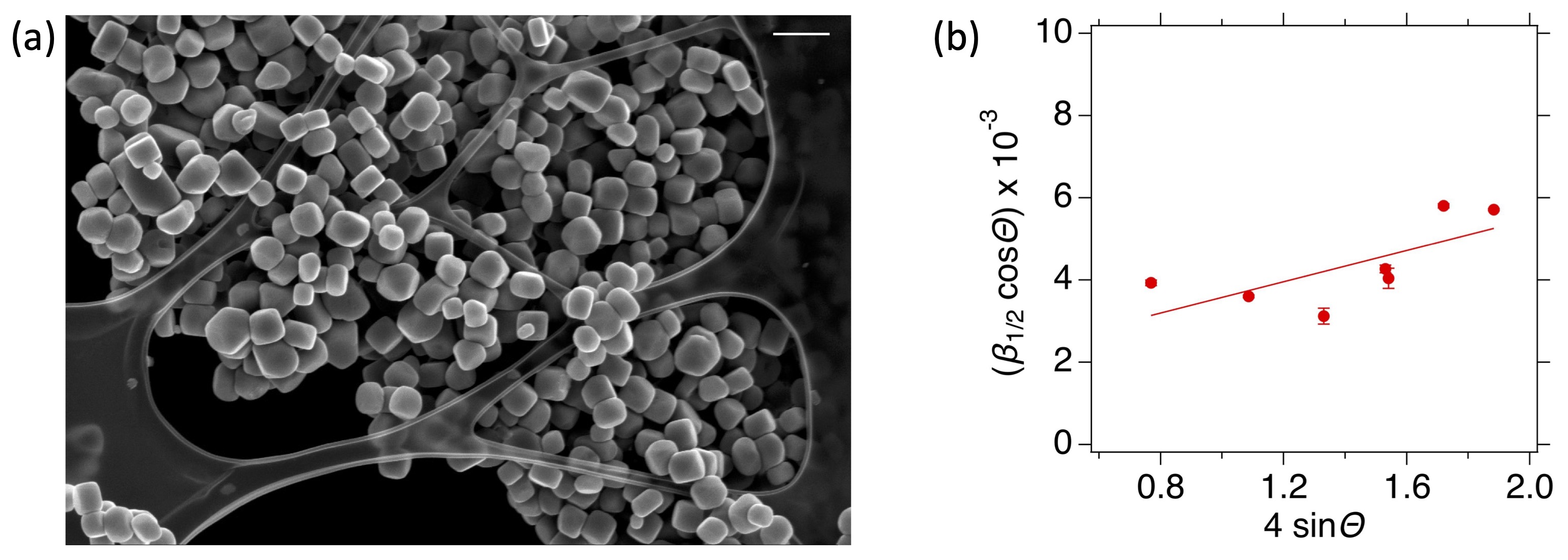
Figure S1a shows a “large” SEM field of view of the as-produced BTO nanocrystal powder. This powder was the starting material to prepare the BTO NC aqueous suspension from which individual particles were isolated. We also estimate the strain from Figure 1a diffractogram of this powder using the Williamson-Hall equation for a Cauchy peak shape:
| (7) |
where is the full-width at half-maximum of each diffraction peak, is the X-ray radiation wavelength (here Å, and the grain size and inhomogeneous strain, respectively, and is a NC form factor that we took equal to 1. Figure S1b displays the experimental points for each diffraction peak and the linear fit according to equation 7, leading to a strain and a crystallographic grain size nm.
4.6.2 HR-STEM Image
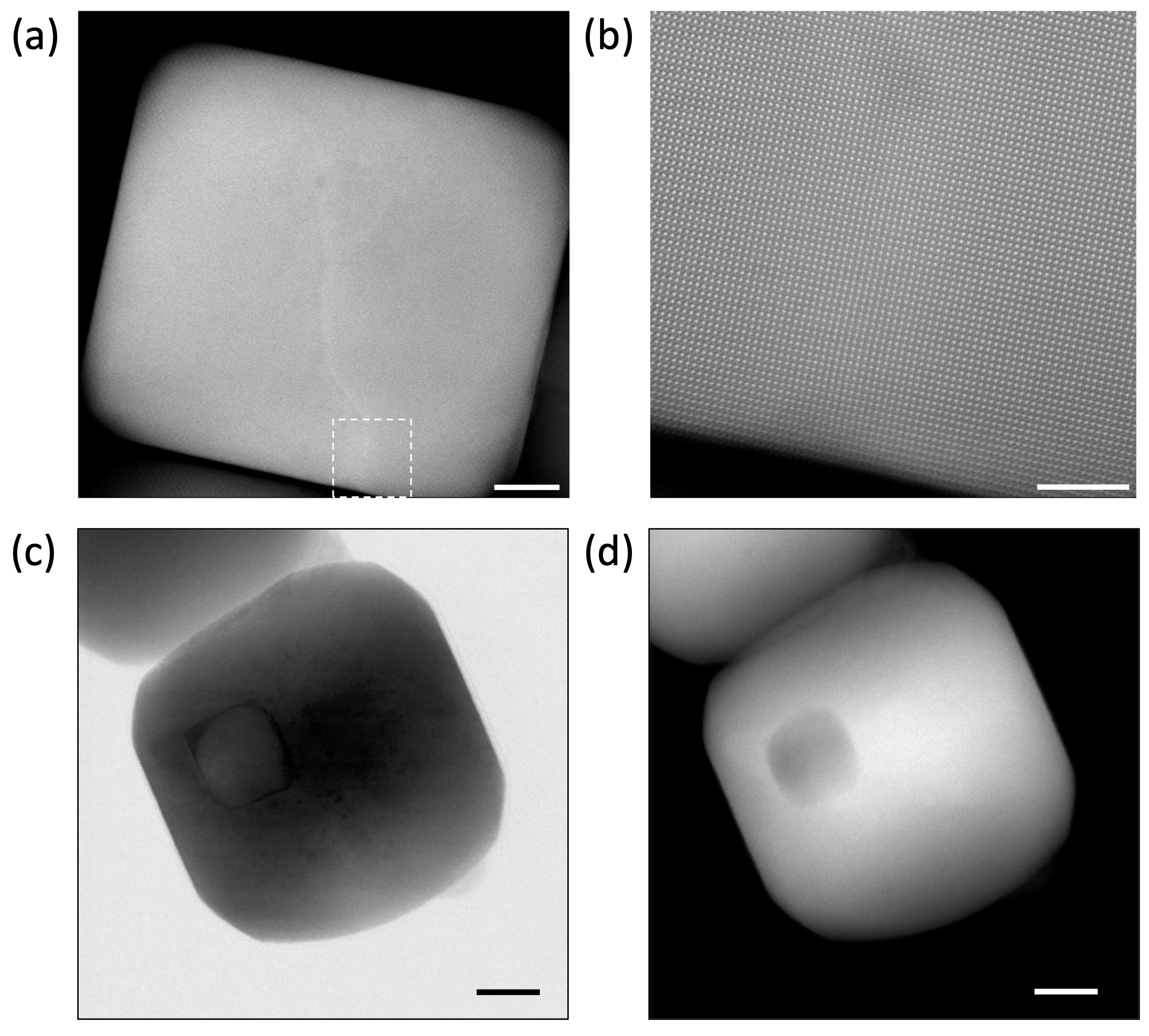
Figure S2 shows HR-STEM images of an individual BTO NC oriented relative to the electron beam to yield atomic column resolution (Figure S2b). We do not observe that the NC has any layer of different crystallographic symmetry than the one at its center. Note that the line crossing the NC from top to bottom on Figure S2a may be either a structural defect or an in-plane domain wall.
4.6.3 Evidence of a phase transition from temperature dependence Raman spectroscopy of BTO nanopowder
4.6.4 Characterization of BTO nanocrystals bound to the substrate
The NC are attached to the numbered grid with a thin layer of PEDOT:PSS conductive polymer. A layer thickness of nm was measured by AFM, as shown on Figure S4a,b, after having removed a tape that had been placed on an edge of the substrate before spin-coating PEDOT:PSS. Similarly, we estimated how much the NC sinks into the PEDOT:PSS before its annealing, by measuring the depth of the hole that remains in the event of the PFM tip drags the NC (Figure S4c,d). We estimate this depth to be nm. The heightened contour encircling the hole is likely to be the concave meniscus that holds the particle, confirming the wetting of the BTO by PEDOT:PSS.
The single NC that we studied by PFM were first identified using SEM and their position in the numbered gold grid, as shown on Figure S5a, allowed to retrieve them in PFM.
For the PFM study, we considered only isolated nanocrystals of close to cubic shape, such as the one in the middle of Figure S5b. Figure S6 shows the size and shape distributions of the isolated NC subsequently studied by PFM.
4.7 2.2. Evidence of non-electromechanical effects and use of electrostatic blind spot setting to suppress them
We evidenced the existence of non-electromechanical effects in PFM measurements and demonstrated their suppression when the laser spot used to measure the cantilever deflection is placed at an electrostatic blind spot (ESBS) position. This approach was first described in Killgore et al. 47.
We first confirmed non-electromechanical effects leading to a PFM signal on an ITO coated substrate alone, with no ferroelectric material deposited on it. These effects were observed through different signatures that were also useful to determine ESBS position by suppressing them in situations where they should not exist, typically on non-ferroelectric materials like in our case the ITO layer. The artifacts observed included the presence of a cantilever contact resonance (Supporting Figure S7a), or a hysteresis loop (Figure S7b), or of a PFM contrast in freshly “written” regions, when the deflection laser spot was adjusted at the extremity of the cantilever, as conventionally done in atomic force microscopy.
As we moved the deflection laser spot further from the cantilever extremity, as shown on the inset picture of Figure S7c, we managed to find a position, the ESBS position, for which the contact resonance disappeared (Figure S7c) and the hysteresis cycle flattened (Figure S7d), removing the previous artifacts.
As mentioned, another type of electrostatic artifact could be detected in PFM phase and amplitude images of ITO surface after having written on a square of 1 m side with +10 and -10 V potentials. Supporting Figure S8a,b shows PFM images with the deflection laser positioned at the extremity of the cantilever just above the tip. Figure S8c,d shows the same region when the laser was positioned between the tip and the ESBS position, showing a decrease in contrast in phase and amplitude signals. Finally, Figure S8e,f shows PFM amplitude and phase images of the same region when we placed the laser at ESBS position (identified by the disappearance of the contact resonance, like in Figure S7c). The absence of phase and amplitude contrast confirms the suppression of electrostatic parasitic effects in the PFM signal.
4.8 2.3. Lateral PFM resonance curve of a cantilever
4.9 2.4. Lateral PFM mapping of three additional BTO NC
4.10 2.5. Additional data on phase field simulations