Electric field tunable superconductivity with competing orders in near magic-angle twisted bilayer graphene
Department of Physics, Indian Institute of Science, Bangalore, 560012, India.
Research Center for Functional Materials, National Institute for Materials Science, Tsukuba, Japan.
International Center for Material Nanoarchitectonics, National Institute for Materials Science, Tsukuba, Japan
Superconductivity (SC) in twisted bilayer graphene (tBLG) has been explored by varying carrier concentrations, twist angles, and screening strength, with the aim of uncovering its origin and possible connections to strong electronic correlations in narrow bands and various resulting broken symmetries. However, the link between the tBLG band structure and the onset of SC and other orders largely remains unclear. In this study, we address this crucial gap by examining in-situ band structure tuning of a near magic-angle () tBLG device with displacement field () and reveal remarkable competition between SC and other broken symmetries. At zero , the device exhibits superconducting signatures without the resistance peak at half-filling, a characteristic signature with a strong electronic correlation. As increases, the SC is suppressed, accompanied by the appearance of a resistance peak at half-filling. Hall density measurements reveal that at zero , SC arises around the van Hove singularity (vHs) from an isospin or spin-valley unpolarized band. At higher , the suppression of SC coincides with broken isospin symmetry near half-filling with lifted degeneracy (). Additionally, when SC is suppressed at higher , density waves around the superconducting dome are seen. These findings, with our theoretical calculations, highlight the competition between SC and other orders, and the stabilization of the latter by the electric field enhanced nesting in the band structure of tBLG.
Introduction:
A relative twist angle between two or more van der Waals layers[1, 2, 3, 4, 5, 6, 7, 8, 9, 10, 11], leading to the formation of moiré superlattice, has opened up a completely new field of condensed matter research known as ‘twistronics’. Observations of interaction-driven emergent phenomena like superconductivity (SC) [1, 12, 2, 6, 13, 14, 15, 16, 17, 18, 19, 20, 21, 8, 9, 10, 11], correlated Mott insulators [3, 2], orbital ferromagnetism [22], anomalous Hall[23] and quantized anomalous Hall effect [24], nematicity [13], chern insulators [25, 26], strange metal [27], giant thermopower [14] and breakdown of semi-classical description of Mott’s formula [14, 28] are ubiquitous in this area. Among the family of twisted heterostructures, magic-angle twisted bilayer graphene (MAtBLG) [1, 2, 3, 29, 12, 30, 13, 25, 26, 27, 17, 19, 31, 32] with a twist angle of between two sheets of graphene monolayer is being extensively studied for hosting flat bands [33] and having a rich phase diagram with such strongly correlated phases. Inter-layer hybridization between the rotated layers facilitates the formation of these isolated flat bands which causes the effective electronic kinetic energy to become much smaller than the effective coulomb interactions [3] leading to the realization of such correlated phases. The appearance of correlated insulators (CI) [3, 2] at integer moiré filling and a superconducting dome when the CIs are doped away from the integer filling [1, 2] shows a strong resemblance to the behavior of high- ( K) cuprate superconductors [34].
Recent studies have, however, raised questions as to whether and to what extent superconductivity in tBLG is intimately connected with correlation effects [17, 18, 16]. In these reports, superconductivity has been observed even in the absence of correlated insulator states by varying the dielectric thickness to control the coulomb screening [17], and even at angles detuned away from , with the SC phase sometimes taking over the whole of the phase space without any signature of correlated states [17, 18, 16]. The decoupling of superconductivity and correlated insulator behavior in the presence of screened coulomb interactions [19] or the increased bandwidth of the flat bands (angles away from ) indicate that these two phenomena may not be always intimately connected, and may even be competing[17, 18] and electron-phonon mechanism may be playing a significant role in the origin of superconductivity in tBLG[17, 35, 36, 37]. Thus, unlike other graphene-based systems such as Bernal bilayer graphene (BBG)[38, 39], rhombohedral trilayer graphene (RTG)[40], ABC-trilayer graphene/aligned with hBN[41], alternatingly twisted trilayer[8, 9], and multilayer graphene[10, 11], where superconductivity consistently emerges close to other symmetry-broken phases, it remains unclear whether superconductivity and other symmetry-broken phases are fundamentally linked in twisted bilayer graphene (tBLG).
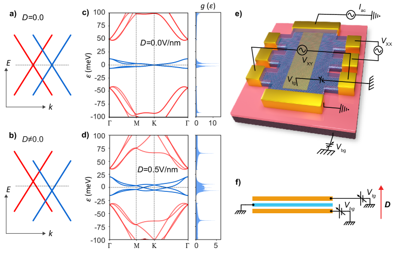
To answer these questions, one needs to investigate specific features of tBLG, other than electron-electron and electron-phonon interaction, e.g., band structure details such as van Hove singularity (vHs) that can crucially influence superconductivity. However, the exploration of how the appearance of superconductivity is connected to the features of such band structure details in tBLG is missing in the literature. Here, we address this issue through the remarkable in-situ tuning of the band structure by a displacement field that continuously tunes a vHs further away from half-filling and thus induces other symmetry-breaking orders, presumably competing with SC. As shown schematically in Fig. 1, applying a perpendicular electric field can tune the band structure of a tBLG with a twist angle slightly away from the magic angle, and can give insights into the intimate connection between the band structure and SC. Thus, we present a comprehensive study on tuning the SC phase of a near-magic angle tBLG () device as a function of a perpendicular electric field (displacement field, ). At zero displacement field ( V/nm), the device shows resistance peaks at the Dirac point (CNP) and full band filling () also known as superlattice gaps, but without any signature of resistance peaks at half-filling (). Most interestingly, the device shows the signature of SC with resistance dropping to almost zero with decreasing temperature away from half-filling ( ). Typical behaviors such as a superconducting dome with temperature (), non-linear current-voltage () characteristics, and suppression of the superconducting phase with a magnetic field () establish the robustness of the SC phase of the device at V/nm. With increasing , the SC phase is suppressed with the appearance of the resistance peak at the half-filling (). The tuning of the SC is further quantified from the dependent critical temperature, , critical D.C. bias current, , and critical magnetic field, , (both parallel and perpendicular). To understand the role of the band structure, we study the Hall density (Hall fillingNormalized Hall density, ) as a function of the filling () at different , which reveals the following: (i) at V/nm, the SC arises precisely around the van Hove singularity (vHs) from an isospin-unpolarized band with degeneracy, , (ii) at higher magnitudes, the suppression of SC is concomitant with the broken isospin symmetry near half-filling, with lifted degeneracy of . Further, when the SC is suppressed at finite , the signature of density waves around the SC dome is seen as periodic resistance oscillations. These observations, along with our theoretical calculations, clearly demonstrate the presence of competing orders in tBLG with different orders stabilized at different electric fields due to the enhanced nesting in the band structure.
0.1 Device set-up and characterization:
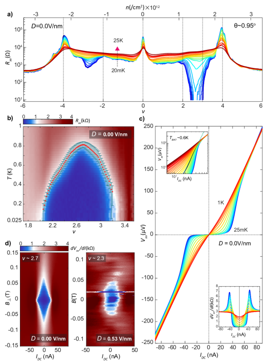
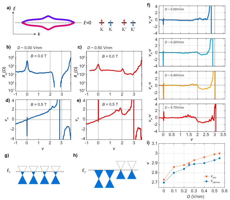
For our study, we have fabricated a dual-gated hBN encapsulated twisted bilayer graphene device using the modified ‘cut and stack’ technique from an exfoliated single monolayer graphene sheet on a SiOSi substrate [42]. Details of fabrication are mentioned in the supplementary information SI-1. A metal layer above the top hBN acts as the top gate of the device, whereas the Silicone (Si) layer acts as the global back gate. The dual-gated device structure helps to tune the number density, , and the perpendicular displacement field, , independently [4, 5, 6, 7, 8, 9] in our tBLG device, as shown schematically in Fig. 1f (see SI-2 for details). Fig. 1e shows the device schematic together with the measurement scheme to measure longitudinal () and transverse () resistance in a standard Hall-bar geometry set-up. Fig. 2a shows the longitudinal resistance, , versus the filling factor, , with increasing temperature from the base temperature of mK up to K at V/nm. The carrier density, , measured relative to the charge neutrality point (CNP) is converted to moiré filling factor, , where is the requisite carrier density to fillempty the low energy flat bands (i.e electronholes per moiré superlattice unit cell) [1, 2]. High insulating resistance peaks at moiré integer filling, , on either side of the CNP indicates the presence of a single-particle band gap above and below the low energy flat bands. The twist angle from the carrier densities for corresponds to for our device, which is around smaller than the magic angle . Note that the twist angle variation across the several contacts remains less than in our device, as shown in SI-Fig.1c,d. Unlike other tBLG devices closer to the magic-angle [1, 2, 3, 12, 17, 18], we do not observe any resistance peaks corresponding to the correlated insulators at half-filling, , or at other integer fillings[2]. All the measurements are done using the standard lock-in technique at Hz in a cryo-free dilution fridge for several thermal cycles.
0.2 Superconductivity at zero :
As seen in Fig. 2a, we see a clear signature of superconductivity on the electron side with the value going down to almost zero between and at the base temperature of mK. Though the signature of resistance decrement with lowering of the temperature on the hole side between and can be seen in Fig. 2a, in this region the value remains finite at the lowest measured temperature ( mK). From here on, we will only focus on the superconducting region on the electron side (). Fig. 2b shows in the d colormap. A superconducting dome around (optimal doping) is clearly visible. The temperature dependence of versus traces are shown in Fig. 2c, which are obtained by integrating as a function of as shown in the lower inset of Fig. 2c. The traces in Fig. 2c show the classic evolution of D superconductors from step-like transitions at low temperature to ohmic dependence around K. The upper inset in Fig. 2c shows the BKT (Berezinskii-Kosterlitz-Thouless) transition, where the evolution of the power law near the critical bias current gives the BKT transition temperature, corresponding to . Fig. 2b and 2c establish the robustness of the superconductivity in our device at V/nm. Further, the superconductivity is killed by applying a perpendicular magnetic field ( mT) as shown in Fig. 2d left panel. Though the Fraunhofer-like oscillation pattern [1, 2, 12, 14, 6, 16, 8] is not seen at V/nm, it is visible when the superconductivity gets suppressed at finite , as shown in the right panel of Fig. 2d (details in SI-4).
0.3 Tuning superconductivity with :
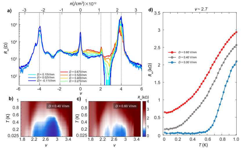
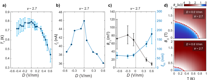
In this section, we discuss our main results on tuning the SC with . Fig. 3a shows the variation of with at the base temperature for several . The corresponding d colormap of with and is shown in SI-Fig. 2a. As shown in Fig. 3a, with increasing positive , the resistance peak values at the CNP and full band filling () slightly decrease while the most dramatic effect with can be seen on the electron-doped side, particularly between . The superconducting region’s width around gradually shrinks as the value crosses V/nm. As SC weakens with , a resistance peak emerges at together with an increase in the background resistance value around . This could be an indication of the onset of correlation physics, which is discussed in the next section while presenting the Hall density measurements. The concomitance between the SC suppression and resistance peak appearance with increasing suggests that the two phases compete rather than being intimately connected. Note that the strength of SC also decreases with negative , but the effect remains weaker compared to the positive as discussed in SI-3 (see SI-Fig. 2b). The superconducting region being tuned by has already been reported in other systems like alternatingly twisted magic-angle trilayer graphene, [9, 8] quadra layer and pentalayer [10, 11] graphene, but not so far seen in tBLG. Ref [12] on MAtBLG reports an appearance of a resistive peak at half filling on the hole side () with increasing , but there are no indications of the modification of the strength of the superconducting phase with . The tunability of the SC phase in our near magic-angle tBLG can be further seen in the superconducting dome, as shown in Fig. 3b and 3c. It can be seen that compared to Fig. 2b at V/nm, at V/nm in Fig. 3c, both the width (in ) of the SC region and are reduced significantly. Fig. 3d shows versus at the optimal doping () for several , emphasizing the tunability of SC with . In Fig. 4, we have summarized the tunability of several SC metrics with . The variation of , , and perpendicular with are shown in Fig.s 4a, 4b, 4c, respectively. Raw data related to these plots are shown in SI-5 and SI-6 (SI-Fig. 4-9); which also describes the method ( value to one-half of its normal state value[2, 6, 8]) used to extract , , and . The right side y-axis of Fig. 4c shows the variation of the superconducting coherence length () with . At a given , the Ginzburg Landau coherence length is extracted from the inferred zero temperature limit of the critical magnetic field, (see SI-6 (IV) for details). Fig. 4d shows the effect on the SC phase of a parallel magnetic field, , and at V/nm (top panel) and V/nm (bottom panel). The temperature dependence of (red dots in Fig. 4d) is fitted to the phenomenological relation: , where is the superconducting critical temperature at zero , and the fitting gives the critical parallel magnetic field in the zero temperature limit, , which matches well with the Pauli limit[6, 29, 8] (see SI-6 (V) for details) at and V/nm. Note that the asymmetry in SC metrics with positive and negative seen in our experiment in Fig. 4 could be related to the asymmetry in the dielectric environment of the top and bottom layer graphene (different thicknesses of the top and bottom hBN, metallic top gate versus SiOSi back gate, and discussed in detail in SI-2 and SI-3), and has been reported for alternatingly twisted trilayer graphene [9, 8].
0.4 Hall density and isospin symmetry breaking with :
So far, we have discussed how the SC is tuned with ; however, to see its connection with the characteristics of the band structure, in this section, we present the Fermiology measurements like the Hall density (). The single particle low-energy band of tBLG has four flavors, corresponding to two valleys and two spins, as schematically shown in Fig. 5a. Fig. 5d shows the variation of the measured Hall filling, (/) (see SI-7 (II) for details), with the moiré filling factor, , at V/nm on the electron-doped side at T (anti-symmetrized by measuring at T, see SI-7 for details). At T, the SC is killed, and it can be seen from Fig. 5b that increases with a linear slope until , and beyond that, increases rapidly and diverges (with value , see SI-Fig. 10a) on either side of , where it changes sign. This is a clear signature of (the Fermi level crossing) a vHs[9]. It can be seen from the versus plot in Fig. 5b ( T) that the SC phase arises around the vHs, and the linear slope in the Hall filling (versus filling) measurement confirms that all the four flavors are equally populated with the charge carriers as shown schematically in Fig. 5g, implying that the SC arises from an isospin-unpolarized band. A similar result for twisted double bilayer graphene stabilized by WSe2 [6] has recently been reported, where the superconductivity emerges from unpolarized states near the van Hove singularities. Fig.s 5c,e show similar plots for V/nm, in which case, initially, the increases with slope one; however, before reaching the vHs at , there is a suppression of around , where a resistance peak () concomitantly emerges as shown in Fig. 5c, with no SC. The d colormap of with and is shown in SI-Fig. 11a. To understand the suppression in Hall filling with , in Fig. 5f we plot versus , which remains close to zero at V/nm, reconfirming the degeneracy of of the occupied bands. As can be seen from the figure, with increasing the values of deviate from zero and become negative between and vHs, and their values head towards , attaining the value of at V/nm, which indicates broken isospin symmetry with as schematically shown in Fig. 5h. The signatures of broken isospin symmetry are also seen in the Landau Fan diagram shown in SI-Fig. 12.
0.5 Competing orders and discussion:
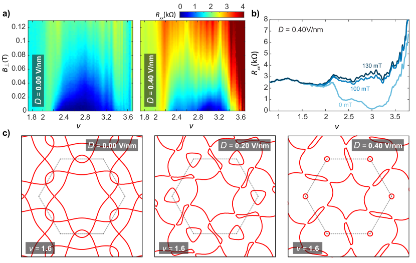
To summarize the above section, for our device, SC arises around the vHs from an unpolarized band but becomes weaker with broken isospin symmetry (or cascaded transitionDi-rac revival) at , which is responsible for the appearance of the peak in . These two competing phases, SC and the phase with isospin polarization are stabilized respectively for small and large values of the displacement field. Though with increasing the SC phase gets suppressed, the intimate connection between the diverging density of states (vHs) and SC can be seen in Fig. 5i, where the filling values corresponding to the vHs () and optimal doping for the SC () are plotted versus and show a close correspondence. In our theory, we capture the shift of the vHs with increasing as shown in SI-Fig. 20. Although the calculated fillings corresponding to the vHs do not precisely match experimental observations, the theory captures the essential features qualitatively. We would like to mention here that there are several other systems, such as rhombohedral trilayer graphene[40], alternatingly twisted trilayer[9, 8] and multilayer graphene[10, 11], in which the SC phase emerges directly from a phase where only two out of the four isospin components are occupied. In comparison, in twisted bilayer graphene, there have been contrasting results between MAtBLG, and detuned [18] or screened tBLG[17, 19]. In this work, in a tBLG slightly away from the magic angle, we have shown that upon tuning with , the two phases seem to compete rather than being intimately connected. Further, in Fig. 6 we show the appearance of other competing orders like density waves arising from spontaneously broken translational symmetry of the moiré lattice when the SC is suppressed at higher [43]. Fig. 6a show how the changes with perpendicular magnetic field, , and at V/nm (left panel) and V/nm (right panel). Nearly periodic oscillations () in become prominent at higher once the SC gets weakened with , which can be seen clearly in Fig. 6a (right panel), and as cut plots in Fig. 6b. The details are discussed in SI-13. These periodic oscillations around the vHs are most likely the manifestation of translation symmetry breaking due to a charge density wave instability and have been reported in the literature[43]. Fermi contours around the vHs in our theoretically calculated band structure offer some insights as to how this comes about. Fig. 6c displays the Fermi contours as computed from a tight binding model (see SI-14 for details). One can see that for higher the contours look approximately like flattened ellipses, with nearly parallel sections signifying nested Fermi contours, (rightmost panel), near the points of the Brillouin Zone. However, such nesting is absent at smaller fields. This indicates the possibility of the formation of charge density waves driven by nesting in the band-structure at finite . In SI-14, we have summarized our theoretical results obtained for various values of fillings, and . Similar tendencies for CDW formation have been predicted previously in MAtBLG[44].
In summary, our findings emphasize the influence of band structure tuning through an external electric field on the emergence of superconductivity and other orders in near magic-angle twisted bilayer graphene. Our results highlight the close connection between the divergent density of states in the electronic structures and the presence of superconductivity. Furthermore, we observe that superconductivity diminishes with alterations to the electronic structure when isospin polarization and density waves are stabilized. Our results are consistent with the recent theoretical study showing the suppression of SC with electric field in tBLG, and highlight how the origin of SC in tBLG is special compared to other twisted and untwisted graphene-based heterostructures[45]. We believe that our study carries broad implications for advancing our understanding of superconductivity as well as other phases in graphitic van der Waals heterostructures, and paves the way for further explorations in the future.
Acknowledgements
A.D. thanks Prof. Ashvin Vishwanath, Prof. Mohit Randeria, and Prof. Nandini Trivedi for the useful discussions. R.D. is grateful to Manabendra Kuiri, Arup Kumar Paul, Ravi Kumar, Saurabh Kumar Srivastav, Souvik Chakraborty, and Ujjal Roy for numerous discussions on the fabrication of twisted heterostructures. R.D. and A.G. thank Ujjal Roy, Saurabh Kumar Srivastav, Ravi Kumar, and Souvik Chakraborty for their assistance while doing measurements in the He3 cryo-stat and cryo-free dilution refrigerator (Oxford Triton and Oxford Proteox). H.R.K. and M.J. gratefully acknowledge the National Supercomputing Mission of the Department of Science and Technology, India, and the Science and Engineering Research Board of the Department of Science and Technology, India, for financial support under Grants No. DST/NSM/R&D HPC Applications/2021/23 and No. SB/DF/005/2017, respectively. H.R.K. also acknowledges support from the Indian National Science Academy under its grant no. INSA/SP/SS/2023/. A.D. thanks the Department of Science and Technology (DST) and Science and Engineering Research Board (SERB), India, for financial support (SP/SERB-22-0387) and acknowledges the Swarnajayanti Fellowship of the DST/SJF/PSA-03/2018-19. A.D. also thanks CEFIPRA project SP/IFCP-22-0005. Growing the hBN crystals received support from the Japan Society for the Promotion of Science (KAKENHI grant nos. 19H05790, 20H00354 and 21H05233) to K.W. and T.T.
Author contributions
R.D. contributed to device fabrication. R.D. and A.G. contributed to data acquisition and analysis. A.G. also contributed to developing measuring codes. S.M., H.R.K., S.B., and M.J. contributed to the development of the theory. K.W. and T.T. synthesized the hBN single crystals. A.D. contributed to conceiving the idea and designing the experiment, data interpretation, and analysis. All the authors contributed to the data interpretation and writing the manuscript.
Competing financial interests
The authors declare no competing interests.
Methods
0.6 Device fabrication and measurement scheme:
The devices consist of hBN-encapsulated twisted bilayer graphene (tBLG) on a SiOSi substrate. The typical length and width of the devices are m and m, respectively. The usual ‘tear and stack’ technique [3, 1] with a modification is used to fabricate the device and is described in detail in the supplementary information (SI-1). We carried out low-temperature transport measurements at mK in a cryo-free dilution refrigerator. Using a constant bias current of nA, the four-probe longitudinal () and transverse voltage () were measured using a lock-in amplifier at a low frequency ( Hz).
0.7 Theory:
A tBLG structure of twist angle was generated using the TWISTER code [46]. The atomic positions were then relaxed in LAMMPS [47] up to a force tolerance of ev/Å. Classical force fields were used to model the interatomic interactions, with Tersoff [48] as the intra-layer potential and DRIP [49] as the inter-layer potential. The electronic band structures were computed using a tight binding model with the transfer integrals approximated using the Slater-Koster formalism [50]. The displacement fields were integrated into the calculations as on-site terms within each layer, enabling the assessment of their impact on the electronic properties of the system. Although the doping levels, at which the van Hove singularities (vHs) occurred in our calculations are lower than those observed experimentally, the qualitative behavior and the evolution of the vHs on the electron side with displacement field are consistent with the experimental findings. Further details are available in the Supplementary Information (SI-14).
0.8 Data availability:
All the relevant non-analytical line-plot data generated or measured during this study are included in this published article (and its supplementary information files). Additional information related to this work is available from the corresponding author upon reasonable request.
References
References
- [1] Cao, Y. et al. Unconventional superconductivity in magic-angle graphene superlattices. Nature 556, 43–50 (2018).
- [2] Lu, X. et al. Superconductors, orbital magnets and correlated states in magic-angle bilayer graphene. Nature 574, 653–657 (2019).
- [3] Cao, Y. et al. Correlated insulator behaviour at half-filling in magic-angle graphene superlattices. Nature 556, 80–84 (2018).
- [4] Liu, X. et al. Tunable spin-polarized correlated states in twisted double bilayer graphene. Nature 583, 221–225 (2020).
- [5] Cao, Y. et al. Tunable correlated states and spin-polarized phases in twisted bilayer–bilayer graphene. Nature 583, 215–220 (2020).
- [6] Su, R., Kuiri, M., Watanabe, K., Taniguchi, T. & Folk, J. Superconductivity in twisted double bilayer graphene stabilized by wse2. Nature Materials 22, 1332–1337 (2023).
- [7] Kuiri, M. et al. Spontaneous time-reversal symmetry breaking in twisted double bilayer graphene. Nature Communications 13, 6468 (2022).
- [8] Park, J. M., Cao, Y., Watanabe, K., Taniguchi, T. & Jarillo-Herrero, P. Tunable strongly coupled superconductivity in magic-angle twisted trilayer graphene. Nature 590, 249–255 (2021).
- [9] Hao, Z. et al. Electric field–tunable superconductivity in alternating-twist magic-angle trilayer graphene. Science 371, 1133–1138 (2021).
- [10] Park, J. M. et al. Robust superconductivity in magic-angle multilayer graphene family. Nature Materials 21, 877–883 (2022).
- [11] Zhang, Y. et al. Promotion of superconductivity in magic-angle graphene multilayers. Science 377, 1538–1543 (2022).
- [12] Yankowitz, M. et al. Tuning superconductivity in twisted bilayer graphene. Science 363, 1059–1064 (2019).
- [13] Cao, Y. et al. Nematicity and competing orders in superconducting magic-angle graphene. Science 372, 264–271 (2021).
- [14] Paul, A. K. et al. Interaction-driven giant thermopower in magic-angle twisted bilayer graphene. Nature Physics 1–8 (2022).
- [15] Codecido, E. et al. Correlated insulating and superconducting states in twisted bilayer graphene below the magic angle. Science Advances 5, eaaw9770 (2019).
- [16] Arora, H. S. et al. Superconductivity in metallic twisted bilayer graphene stabilized by wse2. Nature 583, 379–384 (2020).
- [17] Stepanov, P. et al. Untying the insulating and superconducting orders in magic-angle graphene. Nature 583, 375–378 (2020).
- [18] Saito, Y., Ge, J., Watanabe, K., Taniguchi, T. & Young, A. F. Independent superconductors and correlated insulators in twisted bilayer graphene. Nature Physics 16, 926–930 (2020).
- [19] Liu, X. et al. Tuning electron correlation in magic-angle twisted bilayer graphene using coulomb screening. Science 371, 1261–1265 (2021).
- [20] Tian, H. et al. Evidence for dirac flat band superconductivity enabled by quantum geometry. Nature 614, 440–444 (2023).
- [21] Po, H. C., Zou, L., Vishwanath, A. & Senthil, T. Origin of mott insulating behavior and superconductivity in twisted bilayer graphene. Phys. Rev. X 8, 031089 (2018).
- [22] Sharpe, A. L. et al. Emergent ferromagnetism near three-quarters filling in twisted bilayer graphene. Science 365, 605–608 (2019).
- [23] Tseng, C.-C. et al. Anomalous hall effect at half filling in twisted bilayer graphene. Nature Physics 18, 1038–1042 (2022).
- [24] Serlin, M. et al. Intrinsic quantized anomalous hall effect in a moiré heterostructure. Science 367, 900–903 (2020).
- [25] Wu, S., Zhang, Z., Watanabe, K., Taniguchi, T. & Andrei, E. Y. Chern insulators, van Hove singularities and topological flat bands in magic-angle twisted bilayer graphene. Nature Materials 20, 488–494 (2021).
- [26] Das, I. et al. Symmetry-broken chern insulators and rashba-like landau-level crossings in magic-angle bilayer graphene. Nature Physics 17, 710–714 (2021).
- [27] Cao, Y. et al. Strange metal in magic-angle graphene with near planckian dissipation. Physical review letters 124, 076801 (2020).
- [28] Ghawri, B. et al. Breakdown of semiclassical description of thermoelectricity in near-magic angle twisted bilayer graphene. Nature Communications 13, 1522 (2022).
- [29] Cao, Y., Park, J. M., Watanabe, K., Taniguchi, T. & Jarillo-Herrero, P. Pauli-limit violation and re-entrant superconductivity in moiré graphene. Nature 595, 526–531 (2021).
- [30] Lin, J.-X. et al. Spin-orbit–driven ferromagnetism at half moiré filling in magic-angle twisted bilayer graphene. Science 375, 437–441 (2022).
- [31] Zondiner, U. et al. Cascade of phase transitions and dirac revivals in magic-angle graphene. Nature 582, 203–208 (2020).
- [32] Wong, D. et al. Cascade of electronic transitions in magic-angle twisted bilayer graphene. Nature 582, 198–202 (2020).
- [33] Bistritzer, R. & MacDonald, A. H. Moiré bands in twisted double-layer graphene. Proceedings of the National Academy of Sciences 108, 12233–12237 (2011).
- [34] Xu, Z. A., Ong, N. P., Wang, Y., Kakeshita, T. & Uchida, S. Vortex-like excitations and the onset of superconducting phase fluctuation in underdoped La2-xSrxCuO4. Nature 406, 486–488 (2000).
- [35] Lian, B., Wang, Z. & Bernevig, B. A. Twisted bilayer graphene: A phonon-driven superconductor. Physical review letters 122, 257002 (2019).
- [36] Cea, T. & Guinea, F. Coulomb interaction, phonons, and superconductivity in twisted bilayer graphene. Proceedings of the National Academy of Sciences 118, e2107874118 (2021).
- [37] Shavit, G., Berg, E., Stern, A. & Oreg, Y. Theory of correlated insulators and superconductivity in twisted bilayer graphene. Physical review letters 127, 247703 (2021).
- [38] Zhou, H. et al. Isospin magnetism and spin-polarized superconductivity in bernal bilayer graphene. Science 375, 774–778 (2022).
- [39] Zhang, Y. et al. Enhanced superconductivity in spin–orbit proximitized bilayer graphene. Nature 613, 268–273 (2023).
- [40] Zhou, H., Xie, T., Taniguchi, T., Watanabe, K. & Young, A. F. Superconductivity in rhombohedral trilayer graphene. Nature 598, 434–438 (2021).
- [41] Chen, G. et al. Signatures of tunable superconductivity in a trilayer graphene moiré superlattice. Nature 572, 215–219 (2019).
- [42] Ghosh, A. et al. Evidence of compensated semimetal with electronic correlations at charge neutrality of twisted double bilayer graphene. Communications Physics 6, 360 (2023).
- [43] Lin, J.-X. et al. Zero-field superconducting diode effect in small-twist-angle trilayer graphene. Nature Physics 18, 1221–1227 (2022).
- [44] Isobe, H., Yuan, N. F. Q. & Fu, L. Unconventional superconductivity and density waves in twisted bilayer graphene. Phys. Rev. X 8, 041041 (2018).
- [45] Long, M., Pozo, A. J., Cruz, H. S., Pantaleon, P. A. & Guinea, F. Evolution of superconductivity in twisted graphene multilayers. Private communication .
- [46] Naik, S., Naik, M. H., Maity, I. & Jain, M. Twister: Construction and structural relaxation of commensurate moiré superlattices. Computer Physics Communications 271, 108184 (2022).
- [47] Thompson, A. P. et al. LAMMPS-a flexible simulation tool for particle-based materials modeling at the atomic, meso, and continuum scales. Computer Physics Communications 271, 108171 (2022).
- [48] Kınacı, A., Haskins, J. B., Sevik, C. & Çağın, T. Thermal conductivity of BN-C nanostructures. Physical Review B 86, 115410 (2012).
- [49] Wen, M., Carr, S., Fang, S., Kaxiras, E. & Tadmor, E. B. Dihedral-angle-corrected registry-dependent interlayer potential for multilayer graphene structures. Physical Review B 98, 235404 (2018).
- [50] Moon, P. & Koshino, M. Energy spectrum and quantum Hall effect in twisted bilayer graphene. Physical Review B 85, 195458 (2012).
See pages - of SM