Superconductivity in atomically thin films: 2D critical state model
Abstract
The comprehensive understanding of superconductivity is a multi-scale task that involves several levels, starting from the electronic scale determining the microscopic mechanism, going to the phenomenological scale describing vortices and the continuum-elastic scale describing vortex matter, to the macroscopic scale relevant in technological applications. The prime example for such a macro-phenomenological description is the Bean model that is hugely successful in describing the magnetic and transport properties of bulk superconducting devices. Motivated by the development of novel devices based on superconductivity in atomically thin films, such as twisted-layer graphene, here, we present a simple macro-phenomenological description of the critical state in such two-dimensional (2D) thin films. While transverse screening and demagnetization can be neglected in these systems, thereby simplifying the task in comparison with usual film- and platelet shaped samples, surface- and bulk pinning are important elements to be included. We use our 2D critical state model to describe the transport and magnetic properties of 2D thin-film devices, including the phenomenon of non-reciprocal transport in devices with asymmetric boundaries and the superconducting diode effect.
I Introduction
Technologically relevant superconductors are usually type II materials, with vortices determining their phenomenological properties Abrikosov (1957). In technical applications, the material is often described through its macro-phenomenological properties where vortices appear as an effective medium rather than individual objects. The first such description was the Bean model Bean (1962) that describes magnetic- and transport properties of bulk material in terms of the critical current density due to bulk pinning Larkin and Ovchinnikov (1979), the latter taking the role of a constitutive material relation (here, denotes the magnetic induction that is related to the vortex density , is the superconducting flux quantum, and the vortex separation). A second type of macro-phenomenological description applies to flat samples, e.g., films and platelet-shaped samples as they appeared with the then-novel cuprate superconductors in the late eighties and nineties. Besides bulk pinning Larkin and Ovchinnikov (1979), surface pinning Bean and Livingston (1964); Clem (1974); Benkraouda and Clem (1998); Blatter and Geshkenbein (2008), geometric barriers Zeldov et al. (1994a); Benkraouda and Clem (1996); Brandt (1999); Blatter and Geshkenbein (2008), and demagnetization phenomena Osborn (1945); Brandt and Indenbom (1993); Zeldov et al. (1994b); Blatter and Geshkenbein (2008) become relevant. Today, much interest is focused on atomically thin van der Waals materials Geim and Grigorieva (2013); Novoselov et al. (2016) with superconducting properties Saito et al. (2016), as found in transition metal dichalcogenides Lu et al. (2015); Xi et al. (2016) and twisted layer graphene Cao et al. (2018); Yankowitz et al. (2019). While significant efforts have focused on explaining the microscopic aspects of superconductivity in such atomically thin materials Saito et al. (2016); Qiu et al. (2021); Das et al. (2023); Balents et al. (2020), less emphasis has been devoted to studying the phenomenology of these systems. In the present paper, we introduce a third kind of macro-phenomenological model that describes the two-dimensional (2D) critical state of atomically thin superconductors and use it to determine the relevant transport- and magnetic properties of these materials.
Atomically thin superconductors can easily be tuned, a feature owed to their nanometric thickness. E.g., the surface barrier can be manipulated not only via the geometric design of the edges Clem and Berggren (2011), but also via a finite gate voltage Rocci et al. (2021). In a recent work, the interplay between vortex pinning, the moiré pattern in -layers, and the effects of a perpendicular electric field has been studied Chen et al. (2023), demonstrating the expanded toolkit for engineering superconductivity in this type of materials. This high degree of tunability makes 2D superconductors an ideal platform for realizing interesting and novel devices, see for example the numerous reports on the so-called superconducting diode effect Vodolazov and Peeters (2005); Diez-Merida et al. (2021); Lyu et al. (2021); Pal et al. (2021); Baumgartner et al. (2022); Bauriedl et al. (2022); Golod and Krasnov (2022); Fominov and Mikhailov (2022); Lin et al. (2022); Suri et al. (2022); Gutfreund et al. (2023); Margineda et al. (2023); Sundaresh et al. (2023); Hou et al. (2023); Paolucci et al. (2023); Nakamura et al. (2023); Nadeem et al. (2023); Chen et al. (2023). One important goal of this work then is to provide a simple macro-phenomenological model capable of describing the properties of these 2D materials and their physical performance in technical applications.
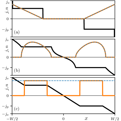
The Bean model has been hugely successfull in explaining the magnetic- and transport properties of the mixed state in bulk material. It reduces the complex pinning behavior of the vortex matter to a simple constitutive material relation . In its simplest (original) variant, is assumed to be independent on the -field (i.e., the vortex density ; we assume ) and solving Maxwell-Ampère’s equation provides the magnetic response of a bulk sample as shown in Fig. 1(a), i.e., the current- and vortex densities and across the superconductor (we assume a finite-width sample along and an infinite extension along ). The simplest critical state is characterized by a constant current density in the penetrated part of the sample that is associated with a linear decrease in (pinned) vortex density away from the sample surface, while both current- and vortex densities vanish inside. Increasing the external field , the vortices penetrate to the middle of the sample (state of full penetration) and the screening saturates with the magnetization . Accounting for surface pinning, the vortex entry into the sample is delayed Clem (1974) and additional layers of Meissner currents flow at the edges, as indicated in Fig. 1(a).
With the emergence of high-temperature superconductors, numerous studies have focused on the phenomenological properties arising from their platelet/film geometry with typical film thickness larger than the London penetration depth . We separate such ‘flat samples’ with from the ‘two-dimensional (2D) thin films’ with , the geometry we will focus on in the present paper, see below. Placing a flat sample () in a perpendicular magnetic field, i.e., with the shortest dimension parallel to the external field , demagnetization effects are strong and the field lines bend around the sample, resulting in Meissner screening currents flowing along all sample boundaries including the top and bottom surfaces perpendicular to the field Brandt and Indenbom (1993); Zeldov et al. (1994b). Furthermore, surface- and geometric edge effects Clem (1974); Zeldov et al. (1994a); Benkraouda and Clem (1996, 1998); Blatter and Geshkenbein (2008) determine the field where vortices penetrate into the sample. In figure 1(b), we illustrate the resulting critical state in flat samples involving Meissner- and vortex-related current densities: since Meissner currents flow on all sample boundaries including the top and bottom surfaces Brandt and Indenbom (1993); Zeldov et al. (1994b, a), vortices are pushed into the sample as soon as the surface/geometrical barrier is overcome; they form two isolated vortex domes where currents flow due to bulk pinning. Meissner currents outside these domes seemingly diverge at the film boundaries (they are cut off at distance from the edge) and connect the vortex-pinning-induced current plateaus across the film center. The magnetic field in direction (evaluated in the film middle at ) vanishes everywhere due to Meissner screening currents, except for the inside of vortex domes and the thin layer at the edges (note the difference between the domes in Fig. 1(b) and the corresponding results in Refs. Brandt and Indenbom, 1993; Zeldov et al., 1994b which is due to the missing of the geometrical barrier in this early work on flat samples: the large Meissner currents at the edges drive vortices, that have overcome the geometrical barrier, to the inside of the film). Hence, a rich critical-state phenomenology (involving conformal mappings and theory of analytic functions in the underlying mathematics Swan (1968); Huebener et al. (1972); Zeldov et al. (1994a); Blatter and Geshkenbein (2008)) characterizes the analysis of flat superconductors that goes beyond the simple description of bulk pinning within the Bean model.
The critical state in 2D thin films with is characterized by the weakness of superconducting screening: as the film thickness drops below the bulk penetration depth , the effective screening length is given by the Pearl length Pearl (1964). For thicknesses in the nanometric range, typical of atomically thin devices, the effective penetration depth is much larger than the coherence length , bringing these materials under the type II paradigm. Even more, easily exceeds the film width , , and the magnetic field remains unscreened, with throughout the film width. This then defines the parametric regime that we focus on in the present paper: 2D thin films with thickness and a finite width such that . This results in the absence of screening and demagnetization effects and allows us to formulate a simple theory for the critical state of such 2D thin-film material that departs significantly from its counterpart in bulk and flat samples, see Fig. 1(c).
While demagnetization and screening can be ignored in 2D thin films with , both surface- and bulk pinning effects play important roles and we will briefly discuss both, one after the other. The vanishing of the current density at the film boundary generates a surface barrier for vortex entry (conveniently described by a fictitious image vortex of opposite circulation) that allows for a surface current density of order of the depairing current density to flow at a distance from the boundaries, i.e., everywhere inside the sample in a typical situation where . Combining Maxwell-Ampère’s and London’s equation (where is the vector potential associated with the induction ) then tells us that the current changes linearly inside the film as long as remains small, . Pushing the external field beyond the surface penetration field drives the current density at the boundaries beyond and vortices enter the film. These are driven towards the film center where they accumulate in the shape of a rectangular box, a ’plateau’ replacing the ‘dome’ in flat samples Zeldov et al. (1994a) of width . As the vortex box expands with further increasing magnetic field , the surface current is squeezed to a narrow layer that reaches the width at the scale of the upper critical field .
In the presence of ‘bulk’ pinning with a finite critical current density , vortices are driven towards the thin-film center as long as the local current density stays larger then . Hence, a symmetric pair of vortex boxes appear away from the boundaries within the 2D thin film as illustrated in Fig. 1(c); they expand with increasing drive and reach the film center (to scale ) at the full-penetration field . As a result, the critical state in 2D thin films differs considerably from those in bulk and flat samples. Particularly noteworthy is the exchange of constant and linear dependencies in the field- and current traces when going between the bulk and the 2D critical states, see Figs. 1(a) and (c), while the comparison between the critical states of flat samples and 2D thin films, see Figs. 1(b) and (c), is of a more quantitative nature. Note that a similar absence of screening characterizes the situation of a thin film with in the parallel-field geometry, see Refs. Shmidt and Mkrtchyan, 1974; Stejic et al., 1994.
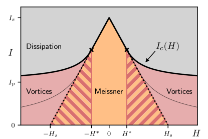
Extending the above critical-state analysis in 2D thin films to include transport currents , we can calculate the critical current of devices in the presence of magnetic fields as shown in Fig. 2. We find that the large currents associated with the surface barrier dominate the current flow and determine the linear field-dependence Maksimova (1998); Plourde et al. (2001); Vodolazov and Peeters (2005) of the critical current at small magnetic fields before vortex entry ( in the absence of bulk pinning), see the solid black line in Fig. 2. At larger fields, vortices occupy a large part of the sample and decreases nonlinearly to a saturation value determined by the bulk critical current density . The figure also informs about the different phases that appear in 2D thin films at given values of field and current , dissipative (grey), Meissner (orange), and mixed (red); the latter two, Meissner- versus mixed states depend on the preparation of the state, here shown is the result of increasing (decreasing) the current from zero (from ) at fixed . A further extension of the model to account for unequal surfaces in asymmetric devices leads us to non-reciprocal transport that is the basis for the superconducting diode effect.
In this paper, we build on previous studies Maksimova (1998); Plourde et al. (2001); Vodolazov and Peeters (2005) to provide an exhaustive description of the 2D critical state model of 2D thin-film superconductors with thickness . In Sec. II, we introduce the 2D critical state model for such 2D thin films based on the Maxwell-London equation that governs the current distribution across such films. We work in the limit typical of atomically-thin strips where we can neglect effects of screening, while fully accounting for both surface- and bulk vortex pinning. We make use of this 2D critical state model to calculate vortex- as well as current-density profiles, first in a finite field without transport, see Sec. II.1, that leads us to Fig. 1(c). In Sec. II.2, we determine the field dependence of the critical current , see Fig. 2, and then find the critical state for a transport current in between. In Sec. III, we determine the non-reciprocal transport properties of asymmetric devices and discuss the superconducting diode effect. We find (in Sec. III.1) that the critical current reaches its maximum at a finite peak field . The different critical currents for positive and negative currents then give rise to the superconducting diode effect. Including bulk pinning, we find an upper bound on the diode efficiency of the 2D thin film even in strongly asymmetric devices, see Sec. III.2. In Sec. III.3, we compare our critical state predictions with recent experiments. While a great deal of transport measurements have been reported on atomically thin superconductors, not much attention has been paid to the magnetic properties of these materials. In the final part of this paper, see Sec. IV, we use our 2D critical state model to determine the hysteretic moment that exhibits numerous features generated by the interplay of surface and bulk pinning. Besides strong experimental signatures, such as kinks, we find a rich variety of vortex configurations such as vortex–anti-vortex coexistence fronts inside the sample. Section V summarizes our results and provides some conclusions.
II 2D critical state model
We consider a thin () superconducting film (in the plane) in a perpendicular magnetic field and introduce a new critical state model to determine the relevant transport and magnetic responses. Inside the superconductor, the current density distribution is determined self-consistently by the interplay of the external field , the distribution of superconducting vortices and the self-field induced by the current density , as given by the Biot-Savart integral. Our 2D thin film has a finite width along and extends to infinity along . For a film of thickness smaller than the London length , the current density is homogeneous in the field direction and we define the sheet current density that depends on the position within the plane of the film. The sheet current density is related to the electromagnetic vector potential and the condensate phase through the London equation
| (1) |
We take the curl of Eq. (1) and rewrite the total field as the sum of the external- and Biot-Savart fields and ; furthermore, we replace the singular gauge part by the vortex density . Accounting for the film geometry and boundary conditions (infinite extension and current along ), the -component of the curl provides us with the Maxwell-London equation Larkin and Ovchinnikov (1971) for the sheet current density
| (2) |
with the -component of the self-field
| (3) |
Equation (2) defines an integro-differential equation for with a characteristic length scale that follows from the comparison of the differential with the self-field term on the right hand side. Estimating the self-field (3) from the current in the absence of screening, see Eqs. (4) and (5) below, we find that . For 2D superconducting strips with , the self-field is negligible and the total magnetic field inside and outside the material has the same value . The equation for the current distribution inside such 2D superconducting thin films therefore simplifies to
| (4) |
a simple first-order differential equation with a source term that depends on the vortex density .
In the following, we will integrate Eq. (4) to find the current-density profile at given field and fixed bias current as summarized in Figs. 3(b)–(e) and 4(b). In doing so, we will determine the critical current as shown in Fig. 2 and characterize the (hysteretic) critical state of thin superconductors with .
II.1 Without bias current
To start with, we consider Eq. (4) in the absence of external bias currents, . In the Meissner state, i.e., when , the current-density profile is linear,
| (5) |
and takes opposite values on the two sides of the 2D film.
Upon increasing the magnetic field , so-called Pearl vortices start penetrating the superconductor; the latter are disk-like objects with supercurrents circulating on the scale that produce a magnetic field of monopolar shape in the upper/lower half-plane, in contrast to the usual flux-tube associated with the Abrikosov vortex in a bulk sample. The nucleation of vortices from the edges of the superconducting film is hampered by the presence of a steep surface barrier. In the ideal scenario, the latter can be overcome by a transport- or field-induced current density when this approaches the depairing current density at the boundary. Indeed, in the narrow 2D film () the self-field can be neglected and the current distribution (at zero field) is homogeneous and equivalent to that in a 1D wire Tinkham (2004), which results in the criterion for the critical surface current density . In real materials, the critical current density where vortices start penetrating inside the superconductor is typically smaller than the depairing value Xu et al. (2010) due to edge roughness, imperfections, or voltage gating Rocci et al. (2021).
In the absence of an external bias current , vortices penetrate inside the sample when the magnetic field reaches the surface penetration value , i.e., when the magnitude of the current density at the edges reaches the critical value . Using Eq. (5), the condition provides us with the surface penetration field
| (6) |
where the superconductor enters the mixed state for . Using the above criterion for the surface current density, the vortex penetration field (6) reads
| (7) |
where the last estimate relates to the thermodynamic critical field that sets the magnetic scale for the penetration of vortices across the surface of a bulk sample in a parallel field Bean and Livingston (1964) (in Ref. Maksimova, 1998, another criterion was used, that resulted in a smaller penetration field , see also Refs. Shmidt and Mkrtchyan, 1974; Stejic et al., 1994 where the same criterion gives for a film in parallel field). Indeed, vortices penetrate inside the thin film when currents of order flow across the full width ; this has to be contrasted with the case of a bulk sample where large currents of order are limited to the London length , what explains the factor in Eq. (7).
In the absence of bulk pinning, the vortices that penetrate inside the 2D film accumulate in a finite region around the center of the superconductor where . In this region, the derivative in Eq. (4) vanishes, implying that the density is constant and given by ; this ‘vortex box’ replaces the ‘vortex dome’ in the flat sample. The solution of (4) then consists of piecewise linear parts near the vortex-free right and left edges, respectively, and a vanishing current in the vortex box; the two solutions merge at the box edges that derive from the condition imposed on the linear part of the solution,
| (8) |
The resulting current-density profile is shown as a red line in the inset of Fig. 3(e) further below.
At finite bulk pinning and large enough fields , vortices from both sides are driven towards the center of the film as long as the local current density stays larger than . Hence, two symmetric vortex plateaus appear away from the boundaries, see Fig. 1(c) in the introduction. The current density is constant and equal to inside these regions and thus the slope in (4) vanishes, again producing the vortex density . Matching the constant current within the plateaus to the (properly shifted) linear current densities (5) in the vortex-free regions, we find the expressions for the inner and outer boundaries and ,
| (9) |
with
| (10) |
the field where the Meissner screening currents (5) reach at the edges of the superconductor.
Summarizing, at small fields below the film remains in the Meissner state (i.e., ) with the linear current profile given by the London response (5). Increasing the field beyond , vortices enter the film and get pinned, with the corresponding current- and vortex-density profiles and shown in Fig. 1(c); note that and do not necessarily coincide any more. The above results will also be relevant in the calculation of the magnetic moment in Sec. IV below, where the hysteretic behavior at decreasing after a field reversal at will be considered as well.
II.2 Critical bias current
We move on to study the critical state preceeding the onset of dissipation, i.e., when a critical current is applied to the superconductor. While the – finite scenario is relevant to magnetization experiments, the critical state with is of great importance for transport experiments.
In the presence of a finite and homogeneous across transport current fed to the sample, the solution of the Maxwell-London equation (4) in the Meissner state picks up an additional term ,
| (11) |
see Figs. 3(b) and (c) where the flat and tilted current distributions at vanishing and finite fields are shown. Note that the linear term induced by the external field does not contribute to the transport current.
Criticality is reached when the magnitude of the current density at either (or both) edges reaches the surface critical current , at which point vortices start penetrating the film. Using Eq. (11), we find the critical current at vanishing magnetic field
| (12) |
with vortices/anti-vortices entering from the two edges. At positive (negative) fields and positive current bias , the screening term in Eq. (11) favours the nucleation of vortices from the left (right) edge of the superconductor when , and the critical current reads Maksimova (1998); Plourde et al. (2001) (we make repeatedly use of Eqs. (6) and (10) to express through or )
| (13) |
Equation (13) defines the critical current in the Meissner state; its linear cusp is the hallmark of surface pinning and corresponds to the linear portions of the black solid line in Fig. 2. The result is valid as long as the current density is larger than depinning everywhere, , allowing vortices to traverse the superconductor without stopping.
The field where first touches then defines a new regime where vortices that enter from the left edge stop because of bulk pinning just before exiting at the right edge. This brings the superconductor to the onset of the mixed state, with the corresponding critical state shown by the solid black line in Fig. 3(c). Imposing the conditions and valid at on Eq. (11), we obtain the relation that sets the transition between Meissner and mixed critical states at,
| (14) |
Increasing the field beyond , the critical current-density profile turns steeper on the left and the mixed state region expands from the right edge into the film, see the black solid lines in Figs. 3(d) and (e). Currents in the linear region push the vortices into the superconductor until they stop and accumulate to form a vortex box with constant density within the region . The Maxwell-London equation (4) then tells that the current density is constant within the vortex box, assuming the value at criticality. Matching the linear and constant portions of , we find the result (see also Appendix A and Eq. (9))
| (15) |
Integrating the resulting current profile , we find the critical current curve in the form (we define and repeat the low-field result Eq. (13); the extension to negative fields is trivial)
| (16) | |||||
| (17) |
The presence of the finite vortex box at fields contributes with the current to , that results in the nonlinear dependence of the critical current on the field . In the limit of large magnetic fields , and saturates to . In the absence of bulk pinning, the critical current drops towards zero as , see Refs. Maksimova, 1998; Plourde et al., 2001. Conversely, as bulk pinning becomes strong, , the linear peak Eq. (16) at small fields, that is due to surface pinning, gets absorbed into the flat background due to bulk pinning. The results (16) and (17) compactly illustrate the relevance of surface and bulk pinning: the surface barrier dominates the low-field regime at and produces a linear cusp in , while bulk pinning shapes the large-field region and produces a saturation in the tails.
When comparing the above theoretical results for to experiments, we note that the magnitude of depends, via , on the value of the critical current density at the edges. The latter can vary from sample to sample due to edge imperfections, rendering the task of predicting the value of the critical current not straightforward. This is not the case, however, for the slope in the Meissner state: taking the derivative of (13), we find that
| (18) |
is independent of . The slope of thus assumes a universal value, determined only by the London length and the width of the film.
II.3 Finite bias current
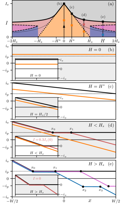
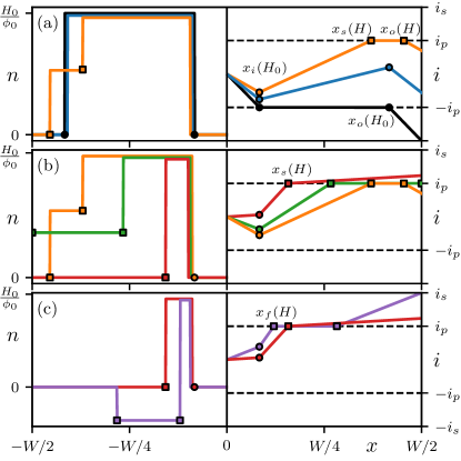
We proceed with the study of the critical state for arbitrary bias current at fixed field . At small fields , the film always resides in the Meissner phase and thus behaves reversibly, with and given by the shifted linear profile (11). At larger fields , the presence of vortices gives rise to hysteretic behavior: we will first study the vortex- and current density profiles and for increasing currents at fixed in samples initially prepared at zero bias current and focus on currents decreasing from in a second step. On increasing from zero at intermediate fixed fields, , the film first displays zero and then one vortex box (with edges ), while it goes from two boxes (with edges ) to one box at larger fields , see the differently colored states in 3(a). Note that the symmetric boxes with coordinates and at vanishing currents are replaced by asymmetric ones involving coordinates to at finite currents .
Without loss of generality, we will consider positive magnetic fields , such that vortices shift towards the right of the superconductor when . To benefit the reader, we will defer the detailed derivations and expressions for the edges of the vortex boxes to Appendix A and focus here on understanding the irreversible evolution of the current-density profile as the bias current is changed from to and reverse.
II.3.1 Increasing the current from
In the absence of bias currents and for fields , the superconductor is in the Meissner state. Upon increasing , vortices first penetrate inside the sample when the current density (11) reaches at either of the two edges, cf. the derivation of (13), i.e., along the line
| (19) |
This (black dotted) line in Fig. 3(a) separates the Meissner- from the mixed states when starting from with and coincides with the critical current (13) at low fields . As a result, for increasing bias currents , the Meissner state encompasses the orange and red-dashed regions in Fig. 2, see also the orange region in Fig. 3(a).
For larger bias currents , vortices accumulate inside the superconductor, forming a vortex box that extends between and ; the box boundaries and are again obtained by matching the linear and constant () portions of the current profile derived from the Maxwell-London equation (4) and fixing the current , see App. A.1. The solution is still given by Eq. (15), while depends additionally on the current and reads,
| (20) |
The first (tiny) vortex box appears on the line : for the current profile touches on the right boundary, , and the first vortex box appears at . With increasing , the current-density profile reaches bulk pinning at values and the nucleation of the vortex box moves to the left. For , we have and the current-density profile cuts at two symmetric points , hence two vortex boxes appear at these latter points, see Eq. (9), with .
The current-density profile for a situation away from is shown in red in Fig. 3(d); the current distribution evolves into the critical one (black lines) as the bias current is increased to and the vortex box touches the right edge of the sample, allowing vortices to leave the superconductor.
For fields , the superconductor is in the mixed state already for vanishing bias currents , with two symmetric vortex boxes and present inside the sample. Upon increasing the bias current, the left box expands, as new vortices enter the superconductor from the left edge, while the right box shifts towards the right edge and conserves its size, as vortices therein are trapped by the surface currents and cannot leave the film. Again, the boundaries of the vortex boxes are found by imposing that (made up from linear and constant portions) is continuous across the superconductor and that ; the corresponding expressions are given by Eqs. (64)–(66) and (55) of Appendix A.1 and a typical current-density profile is shown in blue in Fig. 3(e).
When the bias currents reaches
| (21) |
the boundary of the right vortex box touches and the box starts shrinking as the vortices gradually leave the superconductor. The current-density profile typical for this regime is shown in magenta in Fig. 3(e) and the corresponding expressions for and are given by Eqs. (69)–(70) as well as (55). When , the right vortex box has disappeared completely and only the left box remains; this happens when the bias current reaches
| (22) |
Equations (21) and (22) correspond, respectively, to the lower and upper black dashed curves in the diagram Fig. 3(a). The two curves cross at , where i) the right box touches the sample edge at and ii) its width vanishes. For bias currents , the current-density profile displays a single plateau, i.e., there is only one surviving vortex box whose boundaries and are described by the same expressions (15) and (20) as obtained for fields ; finally, the critical current is reached when .
II.3.2 Decreasing the current from
Due to the presence of a finite vortex population inside the superconductor, the behavior of the mixed state is different when increasing the bias current from zero versus decreasing from , that leads to a hysteretic behavior reminescent of that of the critical state in bulk and flat superconductors Tinkham (2004). Here, we study the situation where the transport current decreases from the critical value at fixed field in order to study the hysteretic effects in current , see Sec. IV below for a study of hysteretic effects in . In preparing the sample, we wish to avoid complications associated with the dissipative state (e.g., a potential strong rearrangement in the current profile ) and therefore drive the film close to, but below before decreasing the current .
Starting with small fields , the film always remains in the Meissner state and hence behaves reversibly. Going to higher fields and preparing the film at , vortices have populated the superconductor such that the sample remains in the mixed state for all values of the bias current , including the red-dashed region in Fig. 2, see also the red region in Fig. 4(a). Decreasing the current below the vortices that are trapped inside the superconductor remain trapped in the region , with given by Eq. (15), see the upper solid black curve in Fig. 4(b), and the local density of vortices does not change as long as remains below its bulk critical value . As a result, the current-density profile is rigidly shifted downwards, see the upper solid red line in Fig. 4(b), until the current in the plateau first reaches at (black dashed line in (a)). At this current, the vortices start shifting to the left and a new vortex-free region with forms close to the right edge of the superconductor (lower solid red curve in (b)); the position of the vortex box in the region is given by Eqs. (72)–(73) in Appendix A.2. Finally, when is further decreased to , the current density reaches at the right boundary in the same instant that touches the left boundary , thus realizing the critical state appertaining to . Hence, in the process of reducing the current from to , the vortex box has kept its size and has shifted from the right side to the left side of the film. Also, note that decreasing the current from critical, the vortex configuration in the mixed state always contains a single vortex box, see Fig. 4(a), different from the behavior with increasing currents where the number of vortex boxes changes between two and one, see Fig. 3(a).
III Superconducting diode effect in asymmetric 2D thin films
Superconducting films have a long tradition in technological applications, including Josephson junction-based devices in electronics and many types of sensors, e.g., for magnetic fields (SQUIDS) or photodetectors (bolometers). Another application that has been much discussed recently is the superconducting diode effect (SDE) Vodolazov and Peeters (2005); Diez-Merida et al. (2021); Lyu et al. (2021); Pal et al. (2021); Baumgartner et al. (2022); Bauriedl et al. (2022); Golod and Krasnov (2022); Lin et al. (2022); Suri et al. (2022); Gutfreund et al. (2023); Margineda et al. (2023); Sundaresh et al. (2023); Hou et al. (2023); Paolucci et al. (2023); Nakamura et al. (2023); Nadeem et al. (2023); Chen et al. (2023) in 2D superconductors. In this type of inductive device, an ac current drive is applied to produce a dc voltage, the opposite of the usual capacitive setup in a semiconductor where an ac voltage drive produces a dc current. A simple mechanism producing this effect is provided by the asymmetric vortex motion within a superconducting film upon current reversal that produces a non-reciprocal transport characteristic. Such a vortex-based SDE can be realized through asymmetric surface barriers generating different surface critical current densities and at the left and right edges of the film, respectively. This kind of asymmetry is ubiquitous in real thin films and can result from device imperfections Plourde et al. (2001) or deliberate design Hou et al. (2023). Another vortex-based source of non-reciprocal transport is the ratchet effect in bulk vortex pinning producing different depinning currents and for vortices incident from the left and right side, respectively. Such a bulk asymmetry does not naturally occur in thin film devices, but can be realized in nanostructured devices Villegas et al. (2003); de Souza Silva et al. (2006); Gillijns et al. (2007); Lyu et al. (2021); Lang (2024) and twisted moiré superconductors Chen et al. (2023), where the degree of asymmetry can directly be controlled by means of an applied gate voltage. While the surface barrier asymmetry manifests in the low field peak of , the asymmetry in bulk pinning shows up in the tails of at large fields.
Alternative mechanisms Nadeem et al. (2023) involving symmetry breaking on a microscopic level have been discussed in order to generate a superconducting diode effect. Prominent examples are noncentrosymmetric materials Hoshino et al. (2018); Ando et al. (2020); Daido et al. (2022), finite momentum pairing Yuan and Fu (2022), or chiral superconductors Zinkl et al. (2022). At the same time, use of the SDE has been proposed as a means to infer spontaneous symmetry breaking in exotic superconductors Zinkl et al. (2022). However, care has to be taken in order not to confuse an intrinsic mechanism with the simple vortex-based origin where time-reversal- and inversion symmetries are broken on a macroscopic level, see Ref. Moll and Geshkenbein, 2023 and the discussion in Sec. III.3 below.
In the present section, we provide a simple and quantitative analysis of the superconducting diode effect in terms of our critical state model, including also the effect of bulk pinning. In Sec. III.1 below, we will first determine the non-reciprocal critical currents and for different drives along and opposite to the -axis. Subsequently, we will find quantitative results for the diode efficiency, see Sec. III.2, and then compare our findings with recent experiments, Sec. III.3.
III.1 Critical current in asymmetric 2D thin films
In the following, we will assume that the film asymmetry is such that the surface critical current density and surface penetration field , see (6), at the left edge are larger than their counterparts and at the right edge. Moreover, for the main part of this section, we will assume that the surface critical current densities are larger than either depinning current, i.e., .
For such an asymmetric setup, criticality at zero-field is realized when the homogeneous current density in (11) reaches the smaller critical value at the right boundary , hence, , see the blue line in the inset of Fig. 5. Vortices then enter the sample from the right side only. Since the application of a field tilts the current profile, the current can be further increased until reaching the critical surface current at the left film boundary, i.e., , at a finite field , see the orange line in the inset of Fig. 5. Using Eq. (11), the two conditions and transform to the relations
| (23) | |||||
| (24) |
The first equation then relates the peak field to the macroscopic difference in the total currents ,
| (25) |
while the sum and differences of the equations (23) and (24) express the macroscopic quantities and through the surface parameters and ,
| (26) | |||||
| (27) |
In a next step, we account for the presence of bulk pinning by repeating the strategy adopted for the symmetric film and compute . Defining and as the right- and left generalizations of the field in Eq. (14), we find that
| (28) |
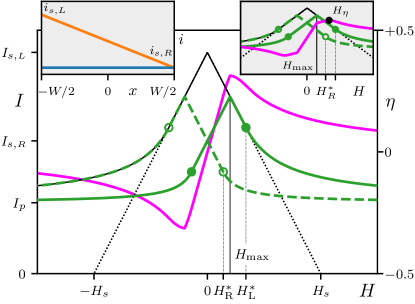
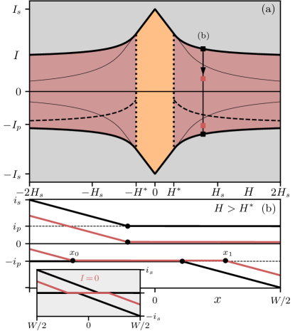
The overall field dependence of the critical current for an asymmetric sample with and symmetric bulk pinning , resulting in a peak field , is shown as a solid green line in Fig. 5. For a current flow in the opposite direction, the left and right surfaces are exchanged and the solid green line in Fig. 5 is reflected with respect to the origin, with the peak field changing sign. Defining and as the critical currents flowing in the positive and negative directions, respectively, we find them related through , as required by time reversal symmetry. The absolute value , the dashed green line in Fig. 5, is thus a mirror copy of reflected with respect to the axis. Asymmetric bulk pinning with results in different asymptotic currents and . Hence, while surface asymmetry manifests in the shift of the peak at small fields, an asymmmetry in bulk pinning manifests in the tails at large fields.
III.2 Efficiency of superconducting diode
Given the difference in the positive and negative critical currents, asymmetric 2D superconducting films display non-reciprocal transport properties that can be exploited in the fabrication of a superconducting diode Vodolazov and Peeters (2005). The non-reciprocal character of these devices is commonly quantified by the (antisymmetric) diode efficiency
| (29) |
shown as the magenta line in Fig. 5; in Eq. (29), we have used that and is given by Eq. (28). As the system obeys time-reversal symmetry, the diode efficiency vanishes for . Moreover, it saturates to the constant value
| (30) |
at large fields where the asymmetric bulk pinning dominates over the effects of surface barriers and reduces to zero for symmetric bulk pinning , see Fig. 5. The sign of indicates the polarity of the diode-like behavior.
The full field dependence is straightforwardly obtained by the expression (28) for the critical current into the definition (29) of , see the magenta line in Fig. 5. Below, we focus on the position of the maximum in the efficiency for the case of symmetric bulk pinning . We start by analyzing the situation at small asymmetry where , shown in the top-right inset of Fig. 5. In this situation, the cusp of at resides within the linear segment of that extends up to . Similarly, drops linearly up to . As a result, the numerator in Eq. (29) stays constant in the interval while the denominator decreases, hence, rises with increasing . With a continuous derivative of across , the efficiency grows further and reaches its maximum at a field where , resulting in
| (31) |
The maximal diode efficiency is then found by evaluating the expression (29) for at this field,
| (32) |
When grows larger, the non-analyticity in at approaches and the above derivation breaks down at . For , the peak in pins the maximum of and hence is achieved exactly at ; we then enter the domain of large asymmetry (shown in the main part of Fig. 5) where
| (33) |
Let us consider how much the diode efficiency can be increased in a strongly asymmetric device (but with symmetric bulk pinning ) by decreasing the strength of the weaker (in our convention, the right) surface barrier until eventually reaching . When this happens, the right edge does no longer play any role as nucleated vortices are stuck until they can overcome vortex pinning in the bulk. The maximal possible diode efficiency is therefore obtained by replacing the right surface barrier with the bulk pinning parameter, i.e., by substituting in Eq. (33), yielding
| (34) |
as the maximal possible in a device with finite (symmetric) bulk pinning.
III.3 Comparison with experiments
The superconducting diode can be engineered in 2D thin films with asymmetric surface barriers as proposed and studied in Ref. Vodolazov and Peeters (2005). This type of inductive diode has recently been realized in conventional films (such as niobium and vanadium) and its functionality has been understood Hou et al. (2023). Here, we will analyze and discuss two recent experimental works Hou et al. (2023); Bauriedl et al. (2022); in both of these studies, the data for the critical current look very similar, but the conclusions drawn by the authors turn out very different. In a first step, we compare the results of our 2D critical state model with their experimental data on the critical current and subsequently discuss the observed efficiency in the light of our findings above. The latter has been used to conjecture Bauriedl et al. (2022) that the diode effect is not vortex based, as the maximum in was found at a field beyond ; as demonstrated above, this finding is nevertheless consistent with our 2D critical-state based vortex model.
We begin with the analysis of as depicted in Fig. 1 of Ref. Bauriedl et al., 2022; the observed curve shows the typical shape expected for a surface dominated sample with a sharp cusp at small fields that compares well with our results in Fig. 5. The experiment was performed in a double layer (thickness and width of the constriction) and clear signatures of non-reciprocal transport and a superconducting diode effect was observed. Transforming the maximal critical current to a current density , we find a value . This has to be compared with the depairing current density that can be obtained from phenomenological parameters and for ; while the bulk value for seems to provide a good estimate (as and in the film are similar to the bulk Chen et al. (2023)), the bulk value may have to be corrected for the film. Taking nevertheless these values, we find a value ; a reduction , here by a factor 5, is expected due to surface imperfections and we consider the agreement quite satisfactory, also with view to our uncertainty in the size of .
Next, we evaluate the slope near the current peak and find a value . This has to be compared with the prediction in Eq. (18) that includes the parameters and . Using the above parameters for and , we find that that results in a small parameter , quite small indeed. On the other hand, we can extract by comparing the experimental result for the slope with the prediction in Eq. (18) and find the value , an outcome that is smaller but still acceptable in comparison with the geometric value . A similar analysis can be carried out for the data reported in Ref. Hou et al., 2023 for their vanadium-based device.
Next, we analyise the experimental data reported for the efficiency. In Ref. Hou et al., 2023, Moodera and collaborators fabricated thin film superconductors with one edge purposefully patterned in order to achieve a strong diode effect. For their vanadium device (Fig. 1 in Ref. Hou et al., 2023) they found that , while from the field dependence of the critical current, we estimate that (we identify the weaker edge on the right). Correspondingly, they report that the diode efficiency is maximal for , see their magenta line in Fig. 1(c). This is in agreement with our theoretical results for a diode device where the maximum in is pinned to the cusp in at .
In Ref. Bauriedl et al., 2022, the edges of the thin film have not been patterned. They find that . This is appreciably smaller than the field that we estimate from their Fig. 1(f). In addition, they reported a maximal diode efficiency at a magnetic field , larger than both and , in agreement with our theory for devices with . Based on this finding, i.e., different peak fields for and , the authors concluded that this would rule out a vortex-based mechanism for the superconducting diode effect. Our analysis tells instead, that this finding is perfectly consistent with our 2D critical state model that explains the diode behavior in terms of weakly asymmetric surface barriers.
The analysis that led to Eqs. (32), (33), and (34) was carried out under the assumption of symmetric bulk pinning. Dropping this condition and assuming asymmetric bulk pinning with , a finite diode efficiency can be realized at large fields, see Eq. (30). Furthermore, it turns out that for a sufficiently large bulk asymmetry, the maximum can be realized in the tails at large fields rather than at or . Moreover, a bulk ratchet effect can give rise to interesting sign reversals of the diode efficiency Gillijns et al. (2007); He et al. (2019); Ideue et al. (2020); Jiang et al. (2021); Margineda et al. (2023). Within our 2D critical state model, such a sign change is naturally explained in terms of opposite asymmetries of surface and bulk pinning, i.e., but . Indeed, since low- and large field behaviors are dominated by surface and bulk, respectively, their change in asymmetry produces a sign change in as the field increases.
IV Magnetic properties of the critical state
We now turn our focus to the magnetic response of 2D thin films with , i.e., we determine the magnetic moment and study the hysteretic trace for a full sweep of the magnetic field along the axis in Fig. 2. The magnetic moment is generated from the currents flowing inside the superconductor and is thus related to the self-field discussed in Eq. (2). As previously announced in Sec. II, magnetization effects are small but nonetheless measurable with sufficiently sensitive techniques, see the discussion in Sec. V below. Moreover, our study of the magnetic response will reveal interesting vortex configurations, such as coexisting vortex- and anti-vortex domains, that should be accessible to magnetic imaging techniques such as, e.g., the SQUID-on-tip Embon et al. (2015).
Standard magnetostatics tells that the magnetic moment of a current distribution is given by the integral
| (35) |
or equivalently, after integration by parts,
| (36) |
where is the induction in the film and the external field. While our approximation was appropriate for the calculation of the current-density profile , here, we have to consider the small difference between and as produced by the current-density profile . Although a magnetization experiment is usually carried out with a squarish sample , here, we keep our 1D geometry with of an elongated film in a perpendicular field to avoid going to a 2D description of the sheet current density . The latter flows along and we find the magnetic moment directed along from (35) to read
| (37) |
where we have included a factor 2 in order to account for the contribution from currents parallel to at the far edges of the sample. Indeed, this last contribution is identical to the contribution from currents parallel to and thus contributes a factor two, in agreement with the result (36) for the total magnetic moment Brandt and Indenbom (1993).
Accounting for the presence of vortices within the type-II film leads to a hysteretic behavior of the magnetic moment . Below, we will first consider the magnetic moment of a pristine (vortex-free) sample in a magnetic field that is ramped up from zero to , entering the mixed state at the penetration field . In a second step, we will reverse the field at a value with vortices trapped within the film and analyze the completion of a full loop in the magnetic moment . We will restrict our analysis to the case of a symmetric thin film with identical surface barriers and symmetric bulk pinning.
IV.1 Magnetic moment: increasing fields
We start with ramping up the external field from zero, as typical in a zero-field cooled (ZFC) experiment. For fields smaller than the surface penetration field , the thin film is in the Meissner state and is given by Eq. (5). Inserting the result into the expression (37), we obtain the magnetic moment in the absence of vortices,
| (38) |
The induction produced by the current density extends a distance of scale in both the and directions and hence resembles the response of a cylinder of diameter and length . Such a cylinder produces the Meissner response (including a demagnetization factor for a cylinder in a perpendicular field ) and expressing the result (38) in terms of the , we find that
| (39) |
One should appreciate that the result (39) is quite large, owing to the fact that we deal with a film in a perpendicular field. Indeed, the response of the film of dimension produces a similar moment as that of a cube with dimensions and there is no geometric reduction. This is different for a film in parallel field, where the moment is down by the geometric factor . The only reduction in (39) is by the factor that originates from the reduced screening due to the small thickness in combination with a restricted film width . For the experiments discussed in Sec. III.3 above, sample sizes are about m and m in Refs. Bauriedl et al., 2022 and Hou et al., 2023, respectively, while m and m, hence the ratio is of order 0.1 – 1.
For fields larger than , two symmetric vortex-boxes as described in Eq. (9) form within the superconductor, see Fig. 6, giving rise to the current-density profile shown in Fig. 1(c). Inserting the (anti-symmetric) current-density profile
| (40) |
into the expression Eq. (37) results in
| (41) |
we arrive at the magnetic moment of the mixed state,
| (42) | |||||
and antisymmetric in . The (negative) magnetic moment as a function of increasing magnetic field is shown as a solid black line in Fig. 7 for . For moderate bulk pinning strengths , see below, the magnetic moment depends on non-monotonically: at small fields , is dominated by the surface barrier contribution and displays a maximum at the onset of the mixed state with
| (43) |
At large fields , the bulk pinning contribution takes over as approaches the asymptotic value
| (44) |
As shown in Fig. 7, the magnetic moment displays a kink corresponding to a finite jump in the derivative when vortices first penetrate. This jump in can be quantified using Eqs. (38) and (42) by comparing the left and right derivatives of the magnetic moment at ,
| (45) |
and
| (46) |
yielding the jump
| (47) |
For negligible bulk pinning , we find the universal result that the right derivative (46) is minus half the left value (45). For larger fields , the absolute value of the right derivative becomes smaller, until it changes sign at . For stronger pinning , the magnetic moment changes monotonically with , with the kink in disappearing as , see the inset of Fig. 7. For larger pinning strengths , the surface barrier does not play any role, as the effective penetration of vortices inside the thin film is determined by the field at which they start moving. This situation can thus be reduced to the case and is described by Eqs. (38) and (42) by substituting with .
IV.2 Magnetic moment: decreasing fields
After increasing the field in a pristine film, we reverse at the value . We will mainly focus on the situation where surface pinning is dominant, i.e., . Reversing the field in the Meissner region , the film responds reversibly. For a reversal field , vortices occupy a finite portion of the thin film and do not immediately leave the sample upon decreasing the magnetic field, see Fig. 6 showing the current density and vortex density profiles in the right and left halves of the film, respectively. The system shows memory effects with the magnetic moment deviating from Eq. (42), resulting in an hysteretic loop as shown in Fig. 7.
The current distribution across the thin film along the irreversible part of the magnetic loop can be obtained by integrating the Maxwell-London equation (4) with the appropriate vortex distribution , see Fig. 6. Inserting the resulting current distribution into the equation (37) for the magnetic moment then produces the curves shown in Fig. 7. To benefit the reader, we will leave the lengthy but straightforward derivations of the analytical results behind these figures to the Appendix B and focus here on understanding the irreversible behavior of , , and from the underlying interplay of surface barrier- and bulk pinning effects.
For a magnetic field just below , the magnitude of the current density in the vortex box drops below . Due to pinning, the vortex density then remains unchanged from the one at and assumes the value within the vortex boxes , see Eq. (9), and zero elsewhere. This is shown on the left part of Fig. 6 with the vortex density at the reversal field (black line) overlapping with the one at (blue line). The Maxwell-London equation (4) then tells that the current displays a negative slope in the vortex-free region and a positive slope in the vortex-boxes, see the blue line in the right part of 6; the corresponding vortex- and current-density profiles are given by Eqs. (74)–(75). Remarkably, and differently from the critical state in the bulk, vortices in this configuration are subject to a finite current density of magnitude smaller than . In this range of magnetic fields, the magnetic moment is given by Eq. (76) that depends linearly on with the Meissner slope (38), see the blue lines in Fig. 7 (with corresponding results at ).
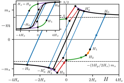
The above state remains valid as long as vortices do not move away from their original positions, i.e., as long as the current-density profile within the vortex box (that has positive slope) remains in the undercritical domain with . As the magnetic field is lowered from , this condition is first broken when , i.e., when takes the value
| (48) |
that determines the transition from the blue to the orange curves in Figs. 6 and 7. Below , the vortex-density profile is changed as the vortices at the outer edge of the box move under the critical force from their original position towards the edge. The vortex box thus devides into high- and low-density parts with densities and , resulting in a two-stage vortex box with a density step at and inner/outer edges at and at . The position derives from tracing the current profile from to (with slope ) to the point (with slope ) where it reaches the critical value ; the condition defines the location
| (49) |
of the density step. As long as the resulting two-stage vortex-box with density and with density does not extend to the film boundary, the total number of vortices remains conserved. To find the box’s outer edge , we impose the condition for vortex number conservation in the form
| (50) |
yielding
| (51) |
The current density inside the region is identical to and assumes a linear slope between and the edges of the thin film. The corresponding vortex- and current densities are given by Eqs. (80)–(81) and are shown in orange in Fig. 6. Due to the conservation of the total vortex number, the areas below the black and orange curves in the plot are identical. The magnetic moment turns non-linear in the interval , see Eq. (82) and the orange segment in Fig. 7. The boundary of this domain is determined by the condition where vortices start leaving the film,
| (52) |
At , we enter the next regime where vortices are free to exit the sample and their number is no longer conserved. The corresponding current- and vortex densities are shown in green in Fig. 6, with the density in the inner (outer) vortex box given by (). The inner boundary and the location of the density step in the two-stage box are still given by and , while the outer boundary is pinned to the edge, ; the vortex- and current-density profiles are given in Eqs. (83)–(84). The constant currents flowing in a large part of the sample produce a reduction in the field dependence of the magnetic moment , see Eq. (85), and the corresponding (green) portion of the magnetic moment in Fig. 7 turns more flat. The orange segment between and connects smoothly the blue and green segments at larger and smaller fields, with no change in the derivative of at and (but a change in curvature).
Vortices continue leaving the film until ; at vanishing field, the density in the outer vortex box has dropped to zero and all vortices at criticality (i.e., where ) have left the film. For negative fields , a thin vortex box with original density survives in the intervals , with still determined by tracing the current profile starting at and using the condition , what results in the expression (49) for . In the remaining part , changes linearly with positive slope , see the red lines in Fig. 6 and Eqs. (86) and (87) for the vortex- and current-density profiles. Within the interval , the magnetic moment changes close to linearly with field and is given by Eq. (88); furthermore, displays a kink at and overshoots the maximal Meissner value given in Eq. (43) close to .
The last hysteretic regime along the magnetic loop is encountered when anti-vortices start penetrating from the film edges. This happens when the above current profile (traced from , see red line in Fig. 6) touches at , resulting in the field
| (53) |
The vortex-density profile again splits into two parts, the leftover vortices with density in the region and the incoming anti-vortices in the region . The vortex–anti-vortex front and the boundary again derive from tracing the current profile with the appropriate slopes, once from till cutting and the other time from where and . The resulting vortex- and current densities are given by Eqs. (89)–(90) and are shown in purple in Fig. 6. At , the magnetic moment curve in Fig. 7 displays another kink and, for sufficiently weak pinning, the slope of changes sign at (see Eqs. (45) and (46) for a quantitative analysis of the kink at ). Correspondingly, the absolute value of starts decreasing again, see Eq. (91) and the purple curves in Fig. 7. Note that the magnitude , i.e., anti-vortices enter the film at a lower field amplitude as compared with the field for vortex entry. Hence, the presence of vortices inside the film lowers the critical entry field for anti-vortices.
As shown with the purple line in the left panel of Fig. 6, in this field regime the vortex- and anti-vortex domains are adjacent to one another at . With further decreasing field , the vortex box is gradually shrinking through incoming anti-vortices—vortex–anti-vortex annihilation then moves the boundary towards the film center until all vortices have disappeared when reaching . This happens at where the entire original vortex box produced at has been replaced by the congruent anti-vortex box and all memory of the field reversal at is erased.
Above, we have implicitly assumed that vortex–anti-vortex annihilation is stabilized at , i.e., by bulk pinning. Indeed, the vortex–anti-vortex attraction quantified by the current density at separation should be (over-)compensated by the bulk pinning current at a scale ; at very weak bulk pinning, grows beyond and an additional vortex-free region separates the vortex box from the anti-vortex box.
So far, we have assumed a reversal field larger than , that implies positive values for the fields and given by Eqs. (48) and (52). Reversing the field at smaller fields , we find that and vortices at immediately leave the film for fields . Correspondingly, the intermediate regimes and are not realized any longer; referring to Figs. 6 and 7 the behavior of , , and jumps directly from ’blue’ to ’red’ at . Note that the current distribution at differs from the one at fields larger than only by the substitution for the outer boundary of the vortex-box.
To conclude this section, let us relax the condition of a strong surface barrier and consider the possibility that bulk pinning prevails with . This corresponds to the scenario where the vortex entry to the film is hampered by bulk pinning and the critical current density does not play any role. As discussed at the end of Sec. III.2, this regime is successfully described with the help of the results from this section upon substitution of with . In this limit, the field reduces to for any value of , as the original vortex box extends to the sample edges and vortices start leaving the sample as soon as they can move from their original positions when the current density reaches the bulk critical value . In addition, when , while when , i.e., for , see the inset of Fig. 7 where . In the first case, the outermost vortices reduce their density as the field is decreased below (the magnetic moment changes from ‘blue’ to ‘green’ type behavior in Fig. 7, see also Fig. 6), and are gradually replaced by anti-vortices as turns negative (‘green’ to ‘purple’ type behavior). In the second, anti-vortices start penetrating into the sample as soon as vortices can escape their pinning centers (direct ‘blue’ to ‘purple’ type behavior). As for the previously considered scenario with , vortex- and anti-vortex domains coexist for . Finally, because anti-vortices replace vortices immediately as these exit the sample at or , the magnetic trace displays no kink upon sweeping the external magnetic field when the surface barrier is weaker than bulk pinning.
V Conclusions
We have presented a 2D critical state model that describes the macrophenomenological properties of 2D thin films with thickness . The geometrically suppressed screening introduces the new characteristic length that easily exceeds the film’s width . In such films with and , the current profile can be found from a straightforward integration of the Maxwell-London equation (4) in the absence of self-field effects (3). The driving term in the Maxwell-London equation (4) depends on the vortex-density profile that we find by including both surface barriers governing vortex entry as well as bulk pinning trapping vortices within the film. The solution of the Maxwell-London equation then involves only linear (Meissner state) and constant (mixed state) segments of current density; together with the vortex profile (made from vortex boxes), these segments are self-consistently combined into the current profile . The results of this 2D critical state model differ pronouncedly from the results of the Bean model describing bulk samples and are quantitatively different from the usual () flat sample macrophenomenology that is dominated by demagnetization- and geometric edge effects.
We have made use of our 2D critical state model to analyze and solve various tasks, the critical current in both symmetric and asymmetric 2D thin films, the determination of the (hysteretic in ) state at arbitrary currents and (fixed) fields , and the hysteretic (in ) magnetic moment . In the resulting phenomenology, effects of surface pinning manifest at small fields, specifically a linear cusp in , Eq. (16), while bulk pinning manifests in the tails of at large fields, Eq. (17). In asymmetric thin films with edges of different surface pinning strength and/or ratchet type bulk pinning, the current transport is non-reciprocal, with the peak maximum in shifted away from zero to , see (25). This non-reciprocity lends itself to the fabrication of superconducting diodes; here, we have extended previous analysis Maksimova (1998); Plourde et al. (2001); Vodolazov and Peeters (2005) to include the effect of bulk pinning and have determined the diode’s efficiency. The comparison with recent experiments shows good agreement between data and theory.
The magnetic moment of 2D thin films has remained uncharted territory so far, both with respect to experiment and theory. While the induced current in the film is small (and can be neglected in the self-field contribution (3) to the Maxwell-London equation), it is this small current that determines the magnetic moment in (37). When surface pinning dominates over bulk pinning, vortex entry into the film manifests as a cusp in the magnetic moment curve , see Eq. (47). Upon reversing the field in the mixed state at , the trapped vortex box evolves in several steps, with field regimes where the box remains invariant, where it splits into two adjacent boxes, where vortices leave as the box reaches the film’s edge and the box shrinks, where anti-vortices annihilate the remaining shrunk box, until all the original vortex box at the field reversal has transformed to a corresponding anti-vortex box at and all memory of the initial state has been lost.
In our study, we have made several assumptions that may be overcome in future work. E.g., we have assumed that the external current is fed homogeneously to the film. In a real sample, though, the contact may feed the current to the film in a non-uniform way, particularly when the contact is small compared to the film width. Second, we remind that our calculation for the magnetic loop has focused on symmetric films, that is the exception rather than the rule as asymmetry in surface pinning occurs quite naturally. Such asymmetry, though, introduces further complexity into the vortex- and current-density profiles, that may be worth analyzing once experiments are being carried out. Furthermore, we have kept the stripe geometry in the calculation of the magnetic moment for simplicity, although typical samples in this type of experiments are rather of squarish shape.
An interesting question is whether and how the current profile and the magnetic moment could be measured in an experiment, as these quantities are small due to the film’s small thickness ; furthermore, the film dimensions (in the m) range are usually quite small. Assuming typical current densities and thicknesses in the few nanometer range, we expect local (parallel) fields of order a fraction of a Gauss (e.g., for ). A correspondingly high sensitivity is provided by the three-junction SQUID on tip (3JSOT) device introduced in Ref. Anahory et al., 2014 that has been developed for simultaneous measurement of parallel and perpendicular (to the film) field components. Using the 3JSOT as a scanning probe at a distance of order above the film, one should be able to image the current-density profile in typical samples with widths from to m, given the reported ac resolution of the device on the order of . Using similar sensitive devices allows to measure the magnetic moment of the film, e.g., via integration of the magnetization map Grover et al. (2022).
Another concern is the application of the macrophenomenological theory to mesoscopic sized samples that appear quite numerously in recent experimental setups. Considering the relevant field scale , see Eq. (7), we can extract a relevant vortex distance , that produces a small number of vortex rows. With typical values and , we arrive at order 10 vortex rows and our simple averaging in a vortex profile may have to be reconsidered. Nevertheless, our results provide a simple and effective first description of the phenomenology of 2D thin films, and improving upon our macro-modelling may require numerical tools.
An interesting observation concerns the non-uniform (linear) current profile that we found in the 2D thin film, a result deriving from the reduced screening. This linear profile contrasts to the usual constant current density profile in the bulk Bean model and may bear interesting consequences when driving the film beyond critical. Indeed, in the dissipative state, flux-flow or normal, we expect a uniform current that is driven by a (uniform) electric field. The transition from the superconducting to the dissipative state in the film then is associated with a sudden rearrangement of the current profile that is expected to give rise to voltage jumps and hysteretic effects.
Acknowledgments
We thank Mikhail Feigelman, Alex Gurevich, and Jagadeesh Moodera for inspiring discussions. We acknowledge financial support of the Swiss National Science Foundation, Division II and the support of the EU Cost Action CA16218 (NANOCOHYBRI).
Appendix A Current-density profile in the mixed state
We derive the current-density profile in the mixed state and obtain the relevant expressions for the vortex-box geometries that are relevant to Sec. II.3. We consider positive magnetic fields , such that vortices accumulate towards the right of the superconductor when . We first consider the situation where the superconductor is prepared at vanishing bias current , as discussed in Sec. II.3.1 and subsequently analyse the scenario where the bias current is decreased from an , see Sec. II.3.2.
A.1 Increasing current from
A.1.1 Fields
The current-density profiles for states prepared from an initial configuration with are shown in Fig. 3. For small fields , the superconductor remains in the Meissner state for all values of the current and no hysteretic effect is present. For larger fields , the superconductor is in the Meissner state when , see Eq. (19), and enters the mixed state at larger currents when and vortices penetrate from the left edge of the film. For , the current-density profile at the left of the film drops linearly from ,
| (54) |
and pushes the vortices to the right; these accumulate in a box with constant current- and vortex densities and . The expression for the left boundary of the vortex box is found by equating in (54) to and we find
| (55) |
independent of and identical to in Eq. (9) with rewritten as , see Eq. (14); the result is applicable in the wide field interval where it takes values between and .
The vortex box extends between and ; to the right of the box, , the current density profile again drops linearly from ,
| (56) |
and the constraint of fixed bias current fixes , that reads
| (57) |
or, after using equation (17) for ,
| (58) |
which touches when . The left and right boundaries (55) and (57) are shown as black dots in Fig. 3(d).
A.1.2 Fields
For larger fields and vanishing bias current , two symmetric vortex boxes (where ) are present inside the superconductor, see Fig. 1(c), the left (right) one extending from to ( to ), see Eq. (9). Upon increasing the bias current , the left box expands to the right as new vortices enter from , while the right one shifts towards with conserved vortex number as the vortices therein are trapped.
To find the positions of the four edges of the vortex boxes, we impose that the current-density profile (involving linear and constant portions as follows from Eq. (4)) is continuous and the total transport current is fixed to . The condition fixes
| (59) |
and the conserved vortex number in the right box, together with Eq. (9) requires that
| (60) |
Finally, the linear portion of between and connects the critical current densities and , hence
| (61) |
which, when replaced to Eq. (60), yields
| (62) |
Integrating the profile , we find the total current
| (63) | |||||
The above equations (59)–(63) determine the four box boundaries as functions of given field and current ; they apply to the regime , see Eq. (21), where the right box is separated from the right boundary, . Inserting from (59) and into (63), we find the current as given in (21). This result for then allows us to write the results for the box boundaries in a compact form,
| (64) |
| (65) |
and
| (66) |
with
| (67) |
The corresponding current-density profile is shown in blue in Fig. 3(e) with the edges of the left and right vortex boxes marked by black dots. For , we have and .
For larger currents, vortices start exiting the right box which gradually shrinks. In this situation, the expression for the total current simplifies to
| (68) |
and using the relations (59) and (61), the new edges of the vortex boxes are found to be
| (69) |
and
| (70) |
Similar as above, we have made use of the expression (22) for , which is to be obtained by the condition for the complete disappearance of the right vortex box and inserting the expressions for and into (68). The current-density profile for is shown in magenta in Fig. 3(e). Finally, when , the right vortex box disappears as , and the mixed state displays a single vortex box described by Eqs. (55) and (58) above.
A.2 Decreasing current from
The presence of vortices leads to hysteretic effects, changing the film’s behavior upon decreasing the bias current from as compared to increasing from zero.
After the state preparation at slightly below for fields , vortices remain trapped in their position as long as the absolute value of the local current density does not exceed . Upon decreasing the bias current , the current distribution is therefore shifted rigidly towards smaller values, see the upper black and red curves in Fig. 4(b), until the current density in the vortex box reaches — this happens when , see the black dashed line in (a). Beyond this point, vortices start rearranging and the vortex box shifts to the left, while maintaining its width and total vortex number. Correspondingly, a new vortex-free region with linear current-density profile is formed close to the right edge (lower red curve in (b)). In this regime, the edges of the vortex box are found by imposing that the current-density profile is continuous and carries the total current
The distance does not depend on and its evaluation at (where is given by (59) and ) produces the condition . Combining this result with Eq. (A.2), we find that
| (72) |
and
| (73) |
The edges of the vortex box in the regime are marked with black dots in Fig. 4(b). Finally, when , the vortex box touches the left edge of the sample, while reaches , and the system has lost any memory of the preparation at .
Appendix B Magnetic moment for a 2D thin film superconductor
Sweeping the magnetic field down from a reversal value , the current distribution across the thin film depends on the vortex density via the Maxwell-London equation (4), with the latter to be determined by the interplay of surface and bulk pinning. Along the magnetic loop, both the current- and vortex profiles change shape as shown in Fig. 6 with separate colors. Inserting the current-density profiles into the definition (37) for the magnetic moment, we obtain for the various regimes, as plotted in Fig. 7 using the same color-coding. In this appendix, we present the analytical expressions for the current- and vortex densities and for the magnetic moments as a function of the magnetic field, thus complementing the discussion in Sec. IV.2 with quantitative results.
B.0.1 Fields
As the magnetic field is reversed at , vortices stay trapped in their original positions , see Eqs. (9), and the vortex distribution is given by
| (74) |
and symmetrically for . This produces the (antisymmetric in ) current distribution
| (75) |
that involves three linear in segments as shown with the blue line in Fig. 6. Integrating the current-density profile as prescribed in Eq. (37) (see also Eq. (41)), we obtain the magnetic moment (shown in blue in the magnetic loop in Fig. 7)
| (76) |
With reference to the piecewise current-density integral, cf. (41), the first and last terms in (76) originate from the film edge at , while the second and third term derive from the vortex box boundaries at and , respectively, see Eq. (9) and use . Making use of the result (42) for the mixed-phase moment in the main text, we can reexpress the above result in the form
| (77) |
to find that the Meissner slope is retraced downwards from the point in the – diagram. This result can be easily understood by inspection of the current-density profile (75) (see also Fig. 6(a)): although vortices are present, they are pinned with a fixed density and box boundaries and that do not depend on . As a consequence, the derivative extends uniformly over the entire width of the film, see Eqs. (4) and (5), that results in a Meissner response.
The vortex distribution changes when the outermost vortex can move again, i.e., for
| (78) |
from which we find the field boundary ,
| (79) |
B.0.2 Fields
Lowering the field below , the outermost vortices rearrange themselves to define a new density profile
| (80) |
and the current distribution reads (we express the bulk critical current by , )
| (81) |
The edges and of the region where vortices redistribute are found by imposing the condition together with the conservation of vortex number (50), see Eqs. (49) and (51). Together, these conditions provide the results (49) and (51) in the main text. At the field , cf. Eq. (52), the outer edge reaches the film surface, , and vortices start exiting the sample. The current- and vortex distributions for fields are shown in orange in Fig. 6 and give rise a nonlinear dependence of the magnetic moment on (shown in orange in Fig. 7),
| (82) |
Again, the first and last terms originate from the film edge , the second and third terms derive from and (note that as given by Eq. (9) changes to given by Eq. (51) when the box splits), respectively, and the fourth term comes from the inner boundary . This association of terms with boundaries will repeat itself also in the expressions below. Furthermore, we note that is continuous at : indeed, the derivatives of Eqs. (75) and (81) match up, as the interval starts appearing only when drops below and is independent of according to Eq. (51).
B.0.3 Fields
Decreasing the magnetic field below , the total vortex number is not conserved as the outermost vortices gradually leave the sample,
| (83) |
with the corresponding critical current densities extending to the sample edges. The full -profile reads
| (84) |
with still given by Eq. (49). Again, the derivatives of Eqs. (81) and (84) match up at : since at , the vortex free region between and disappears and the last region of Eq. (81) is absent. As a result, the derivative is continuous at . This profile remains valid until all vortices in the outermost region have left the film, i.e., until . The vortex- and current density profiles in the field interval are shown in green in Fig. 6. As the current density is constant and equal to in a large part of the sample, the magnetic moment depends only weakly on the field in this regime,
| (85) |
as can be seen by the green curve in Fig. 7. Since the slope in at is absent, see the green line in Fig. 6 left, there is no linear in term in Eq. (85); furthermore, the boundary is absent in this field interval. As discussed in the main text, the above discussion for fields in the interval is valid as long as , i.e., when . Else, the field turns negative and the outermost vortices are expelled from the film as soon as they can move away from their pins.
B.0.4 Fields
Decreasing the field further below , the vortex region shrinks together with and the outermost region turns vortex free,
| (86) |
Correspondingly, the current density is once again linear close to the edges of the sample, with the overall profile taking the form
| (87) |
These results are valid as long as , prohibiting anti-vortices to enter the film, that defines the field as given by Eq. (53). The corresponding vortex- and current densities are shown in red in Fig. 6 and give rise to an approximately linear dependence of the magnetic moment on the field (see the red segments in Fig. 7),
| (88) |
Note, however, that the Meissner slope is spoiled by the field dependence of in (87), cf. Eq. (75) where no such dependence of the vortex density on shows up; furthermore the term is responsible for the deviation from the linear dependence of . The association of terms and boundaries in (88) now involves three terms from and the -term is absent.
B.0.5 Fields
When anti-vortices start penetrating into the thin film for , neighboring vortex- and anti-vortex domains form (if pinning is sufficiently strong), and the vortex distribution reads
| (89) |
where the density is negative in the region , follows from (9) with , and the position of the vortex–anti-vortex front is found the same way as the step position before, i.e., as the point where crosses , hence , see Eq. (49). The current distribution reads
| (90) |
and is analogous to Eq. (81) with the replacement of . As the field is reduced, vortices at annihilate with anti-vortices until and only anti-vortices are left. As discussed in the main text, this happens for . The vortex- and current densities for fields are shown in purple in Fig. 6 and give rise to the magnetic moment (see purple segments in Fig. 7)
| (91) |
References
- Abrikosov (1957) A. Abrikosov, Zh Eksp Teor. Fiz. 32, 1442 (1957), [Sov. Phys. JETP 5, 1174 (1957)].
- Bean (1962) C. P. Bean, Phys. Rev. Lett. 8, 250 (1962).
- Larkin and Ovchinnikov (1979) A. I. Larkin and Y. N. Ovchinnikov, Journal of Low Temperature Physics 34, 409 (1979).
- Bean and Livingston (1964) C. P. Bean and J. D. Livingston, Physical Review Letters 12, 14 (1964).
- Clem (1974) J. R. Clem, “A model for flux pinning in superconductors,” in Low Temperature Physics-LT 13: Volume 3: Superconductivity, edited by K. D. Timmerhaus, W. J. O’Sullivan, and E. F. Hammel (Springer US, Boston, MA, 1974) pp. 102–106.
- Benkraouda and Clem (1998) M. Benkraouda and J. R. Clem, Physical Review B 58, 15103 (1998).
- Blatter and Geshkenbein (2008) G. Blatter and V. B. Geshkenbein, “Vortex matter,” in Superconductivity: Conventional and Unconventional Superconductors, edited by K. H. Bennemann and J. B. Ketterson (Springer Berlin Heidelberg, Berlin, Heidelberg, 2008) pp. 495–637.
- Zeldov et al. (1994a) E. Zeldov, A. I. Larkin, V. B. Geshkenbein, M. Konczykowski, D. Majer, B. Khaykovich, V. M. Vinokur, and H. Shtrikman, Phys. Rev. Lett. 73, 1428 (1994a).
- Benkraouda and Clem (1996) M. Benkraouda and J. R. Clem, Physical Review B 53, 5716 (1996).
- Brandt (1999) E. H. Brandt, Physical Review B 59, 3369 (1999).
- Osborn (1945) J. A. Osborn, Physical Review 67, 351 (1945).
- Brandt and Indenbom (1993) E. H. Brandt and M. Indenbom, Physical Review B 48, 12893 (1993).
- Zeldov et al. (1994b) E. Zeldov, J. R. Clem, M. McElfresh, and M. Darwin, Physical Review B 49, 9802 (1994b).
- Geim and Grigorieva (2013) A. K. Geim and I. V. Grigorieva, Nature 499, 419 (2013).
- Novoselov et al. (2016) K. S. Novoselov, A. Mishchenko, A. Carvalho, and A. H. Castro Neto, Science 353, aac9439 (2016).
- Saito et al. (2016) Y. Saito, T. Nojima, and Y. Iwasa, Nature Reviews Materials 2, 16094 (2016).
- Lu et al. (2015) J. M. Lu, O. Zheliuk, I. Leermakers, N. F. Q. Yuan, U. Zeitler, K. T. Law, and J. T. Ye, Science 350, 1353 (2015).
- Xi et al. (2016) X. Xi, Z. Wang, W. Zhao, J.-H. Park, K. T. Law, H. Berger, L. Forró, J. Shan, and K. F. Mak, Nature Physics 12, 139 (2016).
- Cao et al. (2018) Y. Cao, V. Fatemi, S. Fang, K. Watanabe, T. Taniguchi, E. Kaxiras, and P. Jarillo-Herrero, Nature 556, 43 (2018).
- Yankowitz et al. (2019) M. Yankowitz, S. Chen, H. Polshyn, Y. Zhang, K. Watanabe, T. Taniguchi, D. Graf, A. F. Young, and C. R. Dean, Science 363, 1059 (2019).
- Qiu et al. (2021) D. Qiu, C. Gong, S. Wang, M. Zhang, C. Yang, X. Wang, and J. Xiong, Advanced Materials 33, 2006124 (2021).
- Das et al. (2023) S. Das, H. Paudyal, E. R. Margine, D. F. Agterberg, and I. I. Mazin, npj Computational Materials 9, 66 (2023).
- Balents et al. (2020) L. Balents, C. R. Dean, D. K. Efetov, and A. F. Young, Nature Physics 16, 725 (2020).
- Clem and Berggren (2011) J. R. Clem and K. K. Berggren, Physical Review B 84, 174510 (2011).
- Rocci et al. (2021) M. Rocci, D. Suri, A. Kamra, G. Vilela, Y. Takamura, N. M. Nemes, J. L. Martinez, M. G. Hernandez, and J. S. Moodera, Nano Letters 21, 216 (2021).
- Chen et al. (2023) Z. C. Chen, J. Zhao, F. Gaggioli, S. Grebenchuk, Z. Qiu, Y. Han, J. Hu, K. Watanabe, T. Taniguchi, A. Castro Neto, J. Lu, V. B. Geshkenbein, and K. S. Novoselov, submitted (2023).
- Vodolazov and Peeters (2005) D. Y. Vodolazov and F. M. Peeters, Physical Review B 72, 172508 (2005).
- Diez-Merida et al. (2021) J. Diez-Merida, A. Diez-Carlon, S. Y. Yang, Y.-M. Xie, X.-J. Gao, K. Watanabe, T. Taniguchi, X. Lu, K. T. Law, and D. K. Efetov, arXiv:2110.01067 (2021).
- Lyu et al. (2021) Y.-Y. Lyu, J. Jiang, Y.-L. Wang, Z.-L. Xiao, S. Dong, Q.-H. Chen, M. V. Milošević, H. Wang, R. Divan, J. E. Pearson, P. Wu, F. M. Peeters, and W.-K. Kwok, Nature Communications 12, 2703 (2021).
- Pal et al. (2021) B. Pal, A. Chakraborty, P. K. Sivakumar, M. Davydova, A. K. Gopi, A. K. Pandeya, J. A. Krieger, Y. Zhang, M. Date, S. Ju, N. Yuan, N. B. Schröter, L. Fu, and S. S. Parkin, arXiv:2112.11285 (2021).
- Baumgartner et al. (2022) C. Baumgartner, L. Fuchs, A. Costa, S. Reinhardt, S. Gronin, G. C. Gardner, T. Lindemann, M. J. Manfra, P. E. Faria Junior, D. Kochan, J. Fabian, N. Paradiso, and C. Strunk, Nature Nanotechnology 17, 39 (2022).
- Bauriedl et al. (2022) L. Bauriedl, C. Bäuml, L. Fuchs, C. Baumgartner, N. Paulik, J. M. Bauer, K.-Q. Lin, J. M. Lupton, T. Taniguchi, K. Watanabe, C. Strunk, and N. Paradiso, Nature Communications 13, 4266 (2022).
- Golod and Krasnov (2022) T. Golod and V. M. Krasnov, Nature Communications 13, 3658 (2022).
- Fominov and Mikhailov (2022) Y. V. Fominov and D. S. Mikhailov, Phys. Rev. B 106, 134514 (2022).
- Lin et al. (2022) J.-X. Lin, P. Siriviboon, H. D. Scammell, S. Liu, D. Rhodes, K. Watanabe, T. Taniguchi, J. Hone, M. S. Scheurer, and J. I. A. Li, Nature Physics 18, 1221 (2022).
- Suri et al. (2022) D. Suri, A. Kamra, T. N. G. Meier, M. Kronseder, W. Belzig, C. H. Back, and C. Strunk, Applied Physics Letters 121, 102601 (2022).
- Gutfreund et al. (2023) A. Gutfreund, H. Matsuki, V. Plastovets, A. Noah, L. Gorzawski, N. Fridman, G. Yang, A. Buzdin, O. Millo, J. W. A. Robinson, and Y. Anahory, Nature Communications 14, 1630 (2023).
- Margineda et al. (2023) D. Margineda, A. Crippa, E. Strambini, Y. Fukaya, M. T. Mercaldo, M. Cuoco, and F. Giazotto, Nature Communications 6, 343 (2023).
- Sundaresh et al. (2023) A. Sundaresh, J. I. Väyrynen, Y. Lyanda-Geller, and L. P. Rokhinson, Nature Communications 14, 1628 (2023).
- Hou et al. (2023) Y. Hou, F. Nichele, H. Chi, A. Lodesani, Y. Wu, M. F. Ritter, D. Z. Haxell, M. Davydova, S. Ilić, O. Glezakou-Elbert, A. Varambally, F. S. Bergeret, A. Kamra, L. Fu, P. A. Lee, and J. S. Moodera, Physical Review Letters 131, 027001 (2023).
- Paolucci et al. (2023) F. Paolucci, G. De Simoni, and F. Giazotto, Applied Physics Letters 122, 042601 (2023).
- Nakamura et al. (2023) K. Nakamura, A. Daido, and Y. Yanase, arXiv:2305.19317 (2023).
- Nadeem et al. (2023) M. Nadeem, M. S. Fuhrer, and X. Wang, Nature Reviews Physics 5, 558 (2023).
- Swan (1968) G. W. Swan, Journal of Mathematical Physics 9, 1308 (1968).
- Huebener et al. (1972) R. P. Huebener, R. T. Kampwirth, and J. R. Clem, Journal of Low Temperature Physics 6, 275 (1972).
- Pearl (1964) J. Pearl, Applied Physics Letters 5, 65 (1964).
- Shmidt and Mkrtchyan (1974) V. Shmidt and G. Mkrtchyan, Soviet Physics Uspekhi 17, 170 (1974).
- Stejic et al. (1994) G. Stejic, A. Gurevich, E. Kadyrov, D. Christen, R. Joynt, and D. C. Larbalestier, Phys. Rev. B 49, 1274 (1994).
- Maksimova (1998) G. M. Maksimova, Fiz. Tverd. Tela (St. Petersburg) 40, 1773 (1998), [Physics of the Solid State 40, 1607 (1998)].
- Plourde et al. (2001) B. L. T. Plourde, D. J. Van Harlingen, D. Y. Vodolazov, R. Besseling, M. B. S. Hesselberth, and P. H. Kes, Physical Review B 64, 014503 (2001).
- Larkin and Ovchinnikov (1971) A. Larkin and Y. N. Ovchinnikov, Zh. Eksp. Teor. Fiz. 61, 1221 (1971), [Sov. Phys. JETP 34, 651 (1972)].
- Tinkham (2004) M. Tinkham, Introduction to Superconductivity, Dover Books on Physics Series (Dover Publications, 2004).
- Xu et al. (2010) K. Xu, P. Cao, and J. R. Heath, Nano Letters 10, 4206 (2010).
- Villegas et al. (2003) J. Villegas, S. Savel’ev, F. Nori, E. Gonzalez, J. Anguita, R. García, and J. Vicent, Science 302, 1188 (2003).
- de Souza Silva et al. (2006) C. de Souza Silva, J. Van de Vondel, M. Morelle, and V. Moshchalkov, Nature 440, 651 (2006).
- Gillijns et al. (2007) W. Gillijns, A. V. Silhanek, V. V. Moshchalkov, C. J. O. Reichhardt, and C. Reichhardt, Phys. Rev. Lett. 99, 247002 (2007).
- Lang (2024) W. Lang, “Nanostructured superconductors,” in Encyclopedia of Condensed Matter Physics (Second Edition), edited by T. Chakraborty (Academic Press, Oxford, 2024) pp. 368–380.
- Hoshino et al. (2018) S. Hoshino, R. Wakatsuki, K. Hamamoto, and N. Nagaosa, Phys. Rev. B 98, 054510 (2018).
- Ando et al. (2020) F. Ando, Y. Miyasaka, T. Li, J. Ishizuka, T. Arakawa, Y. Shiota, T. Moriyama, Y. Yanase, and T. Ono, Nature 584, 373 (2020).
- Daido et al. (2022) A. Daido, Y. Ikeda, and Y. Yanase, Phys. Rev. Lett. 128, 037001 (2022).
- Yuan and Fu (2022) N. F. Q. Yuan and L. Fu, Proceedings of the National Academy of Sciences 119, e2119548119 (2022).
- Zinkl et al. (2022) B. Zinkl, K. Hamamoto, and M. Sigrist, Physical Review Research 4, 033167 (2022).
- Moll and Geshkenbein (2023) P. J. W. Moll and V. B. Geshkenbein, Nature Physics 19, 1379 (2023).
- He et al. (2019) A. He, C. Xue, and Y.-H. Zhou, Applied Physics Letters 115, 032602 (2019).
- Ideue et al. (2020) T. Ideue, S. Koshikawa, H. Namiki, T. Sasagawa, and Y. Iwasa, Phys. Rev. Res. 2, 042046 (2020).
- Jiang et al. (2021) J. Jiang, Y.-L. Wang, M. V. Milošević, Z.-L. Xiao, F. M. Peeters, and Q.-H. Chen, Phys. Rev. B 103, 014502 (2021).
- Embon et al. (2015) L. Embon, Y. Anahory, A. Suhov, D. Halbertal, J. Cuppens, A. Yakovenko, A. Uri, Y. Myasoedov, M. L. Rappaport, M. E. Huber, A. Gurevich, and E. Zeldov, Scientific Reports 5, 7598 (2015).
- Anahory et al. (2014) Y. Anahory, J. Reiner, L. Embon, D. Halbertal, A. Yakovenko, Y. Myasoedov, M. L. Rappaport, M. E. Huber, and E. Zeldov, Nano Letters 14, 6481 (2014).
- Grover et al. (2022) S. Grover, M. Bocarsly, A. Uri, P. Stepanov, G. Di Battista, I. Roy, J. Xiao, A. Y. Meltzer, Y. Myasoedov, K. Pareek, K. Watanabe, T. Taniguchi, B. Yan, A. Stern, E. Berg, D. K. Efetov, and E. Zeldov, Nature Physics 18, 885 (2022).