Nonlinear behavior of area dependent interface type resistive switching devices
Abstract
Nonlinearity is a crucial characteristic for implementing hardware security primitives or neuromorphic computing systems. The main feature of all memristive devices is this nonlinear behavior observed in their current-voltage characteristics. To comprehend the nonlinear behavior, we have to understand the coexistence of resistive, capacitive, and inertia (virtual inductive) effects in these devices. These effects originate from physical and chemical processes in memristive devices. The physics-inspired compact model is employed to model and simulate interface-type RRAMs such as Au/BiFeO3/Pt/Ti, Au/NbxOy/Al2O3/Nb, while accounting for the modeling of capacitive and inertia effects. The proposed model’s current-voltage characteristics align well with experimental data and accurately capture the non-zero crossing hysteresis generated by capacitive and inductive effects. The study examines the response of both devices to various frequencies, showing a shift in their nonlinear behavior as evidenced by a reduction in their hysteresis range. Fourier series analysis utilizing a sinusoidal input voltage of varying amplitudes and frequencies indicates harmonics or frequency components that considerably influence the functioning of RRAMs. Moreover, We propose and demonstrate using the frequency spectrum as a fingerprint for memristive devices.
Introduction
While CMOS devices have been the backbone of electronics for decades, memristive devices have emerged as a promising alternative with distinctive characteristics. Memristive devices exhibit intrinsic non-linear behavior, as evidenced by the pinched hysteresis in their current-voltage characteristics, a well-established fingerprint defining their unique attributes [1]. These devices retain information about the amount of charge that has passed through them, presented in the history-dependent resistance function [2, 3, 4]. As the charge accumulates, the resistance (conductance) of the memristor can alter, and this modification is retained until the charge is reset.
Unlike the three traditional circuit components (resistor, capacitor, and inductor) that possess linear relationships between voltage and current, memristive devices display non-linear behavior. The functioning of these devices relies on their internal state, which evolves over time and leads to intriguing and intricate non-linear characteristics [5]. The physical and chemical mechanisms that contribute to resistive switching, such as redox reactions, drift-diffusion of mobile defects, and filament formation[6] change the internal state of the device and thus the resistance of memristive devices. In nanoscale electronic devices, nonlinear behavior can arise from various unknown sources beyond variable resistance. While memristive devices have prominent variable resistance, capacitive and virtual inductive effects can also contribute significantly to non-linearity. To be more specific, the inductive effects are not real and are correlated and referred to as the inertia effects, as described by Yarragolla et al.[7, 8]. A detailed explanation is provided in subsequent sections. As a result, we could say that resistive, capacitive, and inertia memory coexist in such devices [9].
The nonlinear behavior serves as the most important feature that is crucial for implementing neuromorphic dynamic systems such as memristive reservoirs, memristive oscillatory neural networks, and memristive chaotic systems [10]. Furthermore, the non-linear behavior can be strategically utilized as a valuable entropy source for implementing hardware security applications such as physical unclonable functions (PUFs) or true random number generators (TRNGs) [11, 12]. By taking advantage of this behavior, the specific resistive states, transition patterns, harmonics and resonant frequencies of memristive devices can be used as intrinsic and device-specific features. These characteristics, which are challenging to replicate or predict, can be utilized to create cryptographic keys, seeds, or true random numbers with high entropy. Although nonlinear behavior may be an important aspect, it presents several obstacles to overcome, such as achieving reproducibility and reliability in the face of unavoidable variability and ensuring stability and predictability in dynamic synaptic-like plasticity. These challenges require adequate investigation before pursuing practical and effective implementation of memristive devices. Therefore, comprehending the origin and examining the non-linearity of memristive devices is imperative for their efficient utilization in neuromorphic computing and hardware security. One commonly used method is to examine the current-voltage ( I-V) characteristics to identify hysteresis loops that indicate nonlinear behavior. Furthermore, conducting a parametric study that investigates the variations in resistive switching of the device resulting from diverse inputs and device parameters, coupled with Fourier analysis of the frequency spectra, can uncover harmonics and sidebands, thereby offering valuable insights into the non-linear dynamics. Modeling is essential to study and mitigate these challenges by providing a digital platform to explore the effects of various parameters on nonlinear behavior, facilitating the design of memristive devices for optimal performance in neuromorphic computing and hardware security applications.
Memristive devices often exhibit a pinched hysteresis in their current-voltage characteristics, with a zero crossing indicating zero current for zero input voltage. However, some devices, particularly RRAMs, display non-zero crossing hysteresis, suggesting the presence of stored charge. Several studies attribute this phenomenon to resistive, capacitive, and/or inertia effects. So, a more appropriate approach would be to consider the change in resistive switching as a shift in memristive device impedance rather than just memristance. This modification reflects the interplay of different effects, which introduces frequency-dependent impedance, resulting in non-linearities and intricate responses to sinusoidal inputs.
Additional evidence supporting the existence of these effects is shown in Nyquist plots of their impedances, which display double semicircles. One semicircle can be attributed to the presence of an RC circuit, while a negative curve could be interpreted as an inductive loop. It is important to note that this inductive behavior does not correspond to conventional electromagnetic inductance. Instead, we propose that it arises from inertial effects, which contribute to the formation of the second curve. The appearance of different semicircles in a Nyquist plot indicates the presence of multiple time constants or frequency-dependent behavior in a system. Therefore, the coexistence of resistive, capacitive, and inertia effects in memristive devices can result in diverse behaviors at distinct frequencies. Therefore, it is believed that utilizing the frequency-dependent characteristics of memristive devices instead of the commonly used current-voltage characteristics can offer distinct fingerprints. This paper serves as a proof of concept for using the frequency spectrum as an alternative fingerprint to identify and characterize memristive devices. Modeling and simulation techniques are utilized to obtain the frequency spectrum of different devices, enhancing our understanding of the circuit’s overall nonlinear behavior.
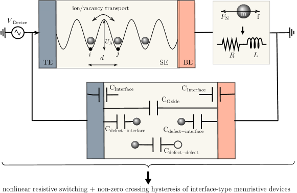
From the previous discussion, it is critical to consider both particle (ion/vacancy) transport and capacitive effects when modeling memristive devices. These two components contribute significantly to the dynamic alterations in memristance. Capacitive effects, encompassing charge storage, and redistribution within the device, are particularly imperative and play a pivotal role alongside ion transport mechanisms. The capacitive components of the device react as the charge accumulates or depletes, impacting the charge distribution and, subsequently, the resistance state. The dual contribution of ion transport and capacitive effects enhances the nonlinear properties observed in memristive devices. Understanding the capacitive contributions is critical to comprehending the complex dynamics that result in non-volatility, hysteresis, and memory-dependent changes in resistance. A deeper understanding of the non-linear behavior of memristive devices can be achieved through comprehensive modeling of ion transport and capacitive effects. Inertia effects are not modeled independently in this work but are included through particle transport. Subsequent sections provide details on how inertia effects are integrated into the overall model for a comprehensive interpretation.
The paper examines the nonlinear behavior of interface-type memristive devices, utilizing a cloud-in-a-cell (CIC) scheme-based model for the Double Barrier Memristive Device (DBMD) [13] and the Bismuth Ferrite Oxide Memristive Device (BFO) [14, 7]. Unlike the state-of-the-art compact models, this method more precisely incorporates the stochastic ion or vacancy transport like the multidimensional computational models, it is fast and accurate like the state-of-the compact models. This study aims to develop a precise model for interface-type devices, considering capacitive effects, as the first step in understanding their nonlinear behavior. Therefore, to study the non-linear behavior, the CIC models proposed by Yarragolla et al.[13, 14, 15] are further modified to incorporate the capacitive effects. The following section will provide a detailed explanation of the modeling of capacitive effects in interface-type memristive devices.
Simulation approach
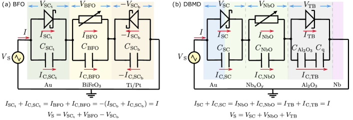
In the interface-type Au/BiFeO/Pt/Ti BFO device [16] and Au/NbO/AlO3/Nb [17], resistive switching occurs through the drift-diffusion or trapping-de-trapping of charged defects, involving positively charged oxygen vacancies in BFO and negatively charged oxygen ions in DBMD. This mechanism alters the properties of the metal/oxide interface (Schottky or tunneling contacts), leading to an analogy-type switching. The primary simulation models for DBMD and BFO devices, utilizing the CIC approach, have been detailed in [13] and [14], respectively.
The CIC method [18] is utilized to examine the behavior of particles in metal oxides, which contributes to resistive switching in RRAMs. This technique involves dividing the RRAM device into a lattice-like grid of cells, with each cell denoting a small volume within the device. Particles, representing atoms, ions, vacancies, or electrons, create a cloud around their positions, distributed across the grid with weights dependent on the oxide defect density. Weight represents the number of actual particles that each simulated particle denotes and allows for modeling a larger population realistically with fewer simulated particles. The weight is calculated as the ratio of total actual particles to simulated ones, which addresses computational limitations. For an input voltage bias, the particles are transported based on their drift velocity, calculated using the activation energy, , and electric field, , obtained by solving the Poisson equation. The drift velocity is calculated as follows based on the probability of the particle movement from one lattice site to another [19, 20]:
| (1) |
where is the lattice constant, is the phonon frequency and is the charge number of the ion/vacancy.
Once the ion or vacancy transport is completed, the electrical parameters, such as the currents and voltages across different layers, are calculated. To incorporate the capacitive effects, parallel capacitors are added across different layers in the equivalent circuit models of BFO and DBMD, as illustrated in Fig. 2.
The resistive current through the Schottky contact is computed as follows [21]:
| (2) |
Here is the effective ideality factor, is the effective Schottky barrier height, and is the effective Richardson constant, is the Boltzmann constant, is the elementary charge and is the temperature. The current across tunneling barrier is calculated using the general Simmons current equation [22].
| (3) |
where is the tunnel barrier height, tunnel barrier width, is the device area and . , , and are the correction factor, free electron mass, and the Planck constant. Moreover, the current across the oxide region is given by the general Ohm’s law,
| (4) |
where is the length of the active oxide layer and is its conductivity. Here, ’ox’ denotes either or oxides. The variables with the subscript ’eff’ represent their effective values, which are derived from the device’s internal state, and rate constant . For more information, refer to the detailed explanation provided by Yarragolla et al.[13].
| Component | depletion layer | capacitance | current |
|---|---|---|---|
| Schottky contact [23] | |||
| Tunneling contact [24] | , | ||
| Oxide |
Capacitive effects
The memristive device contains distinct capacitance elements that serve specific functions in different regions. The proposed model for an interface-type memristive device illustrates four categories of capacitive components as in Fig. 1: (a) capacitance between the interface and defects, (b) between positive and negative defects, (c) oxide capacitance, and (d) interface capacitance. These devices typically have Schottky or tunneling contacts as interfaces. The methods for modeling capacitance across these interfaces are detailed, and corresponding equations are provided in Table 1.
(a) Schottky Contact: The capacitance of a Schottky contact is affected by the dynamics of the depletion layer, a region at the metal-semiconductor interface that lacks charge carriers. Variations in the effective width of the depletion layer , caused by charge accumulation or depletion, affect the overall capacitance [23]. A positive voltage narrows the depletion layer, while a negative bias widens it, thus affecting the capacitance. The depletion layer’s width can be determined by assessing charge accumulation due to traps at the interfaces between the metal and insulator [25]. To determine the capacitance of the Schottky junction , use the electrostatic capacitance equation for a parallel plate capacitor.
(b) Tunnel Barrier: The capacitance across a tunnel barrier can be calculated by considering the series combination of oxide capacitance and quantum capacitance [26]. The oxide capacitance represents the traditional capacitive effects associated with the change in width of the oxide layer , here in DBMD it is . The quantum capacitance accounts for the quantum mechanical effects related to the density of states () in the semiconductor material. Quantum capacitance arises due to the changes in the density of states near the Fermi level in the semiconductor [24]. As the density of states varies, the quantum capacitance reflects the system’s response to changes in charge distribution. The equation used for calculating the quantum capacitance and oxide capacitance in this work is given in Table. 1. The density of states is considered a constant term in this work for simplicity and is calculated based on the capacitance across the tunnel barrier measured by Hansen et al. To simplify calculations, this study does not calculate the density of states. However, simulation methods such as density function theory can be used to calculate it. On the other hand, considering quantum capacitance depends on the particular characteristics of the material, structure, and dimensions involved. Quantum capacitance is more significant in two-dimensional (2D) materials and structures with prominent quantum confinement effects. For very thin layers like a tunnel barrier with a thickness of less than 2 nm, quantum effects become essential.
(a) Metal Oxide: The standard electrostatic capacitance equation is used to determine capacitance across a solid-state electrolyte. This equation considers the effective capacitance resulting from interactions between charged defects and the interface and among different charged defects. The depletion layer width, , indicates the average relative distance between the positions of mobile defects.
Capacitance is typically multiplied by the roughness factor, a dimensionless quantity that indicates the deviation of the real surface area from the ideal geometric surface area. Similarly, a correction factor is applied to the electrostatic capacitance of various RRAM layers to adjust simulation results with experimental findings. This correction factor serves to compensate for several non-idealities inherent to nanoscale devices. Factors such as heterogeneous dielectrics within the oxide layer, interface effects between the oxide and adjacent materials, capacitance frequency dependency, variations in oxide thickness, quantum effects at the nanoscale, and process-related variability can collectively affect electrostatic capacitance. The value of , could be any number between 0 and 1, signifying a reduction in capacitance, accounting for non-idealities and deviations from theoretical expectations. By iteratively adjusting the correction factor, a best-fit value is sought that minimizes the discrepancy between theoretical and experimental results across different conditions and configurations.
Inductive effects
A previously published meminductance model, which is controlled by flux or current and dependent on the system state, has been established in the literature[27, 28]. Although Qingjiang et al.[9] showed various effects in memristive devices, their use of the meminductance model may not be practical or accurate in simulating real-world devices. The assertion of electromagnetic inductance in nanoscale devices may not align with physical constraints, particularly when related to the state equation and a change in inductance proportional to the square of the number of turns. The existence of an additional semi-circle in a Nyquist plot with negative impedance values is attributed to inductive or negative capacitive effects. Marquardt et al.[29] noted that physically realizing windings of an inductance of the required size (>10 mH) within a multi-layer system of approximately 10 nm thickness becomes impractical. However, Bisquert et al.[30] recently proposed a chemical inductor model that is non-electromagnetic, using an inductor and resistor to emulate these effects. While acknowledging the viability of an inductor and resistor model, we propose that the observed combination of inductive effects may be attributed to the inertia of charged particles. As explained by Yarragolla et al.[7], this perspective aligns with the understanding that charged particles exhibit reluctance to change motion, similar to the principles of inertia, contributing to the observed inductive behavior in memristive devices.
In solid-state physics and electronic devices, the behavior of charged particles undergoing resistive switching mimics that of electrical circuits. The movement of these particles, considering drift velocity and friction, is encapsulated in a momentum conservation equation, notably expressed as . This equation, when extended to the drift velocity equation and then to a generalized Ohm’s law (), forms the foundation of the Drude model for electrical conduction. Transitioning further, the equation for drift velocity, when applied to a one-dimensional scenario, yields the final expression[7, 8] {ceqn}
| (5) |
The Drude model explains electron behavior in a conductor through two crucial parameters: kinetic inductance and electrical resistance . Kinetic inductance arises from the inertia of electrons, which causes a delay in their response to an electric field. Electrical resistance, on the other hand, results from collisions between electrons and lattice ions, impeding current flow and causing energy dissipation as heat. The Drude model concepts provide a basis for understanding the electrical properties of conductors at a macroscopic level. They offer insights into how conductivity is affected by external stimuli.
In our model, we account for kinetic inductance by considering the movement of charged particles relative to their drift velocity in Eq. (1), which is influenced by the activation energy of the oxide lattice and the probability of jumps. We have omitted collision effects in our model, so the resistance term can be ignored here. The equation for drift velocity effectively describes the average motion of ions and vacancies in response to an electric field, incorporating momentum-related inertia effects (virtual or kinetic inductance). This integrated approach streamlines the model, eliminating the need for a separate evaluation while explaining the intricate motion of charged particles within an oxide.
Results and discussion
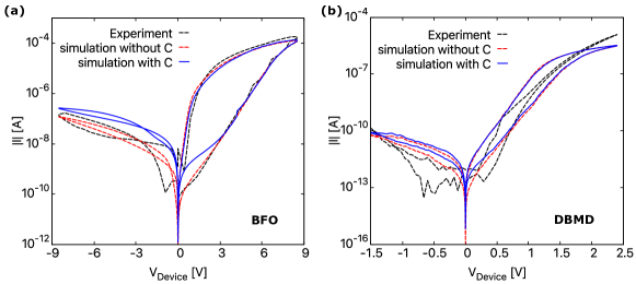
The current-voltage characteristics (I-V curves) shown in Fig. 3 illustrate the nonlinear behavior of BFO and DBMD devices resulting from the coexistence of resistive, capacitive, and inertia effects. To obtain the I-V curves of BFO device shown in Fig. 3(a), an input voltage of 8.5 V was utilized, in conjunction with the parameters used by Yarragolla et al.[14]. The figure compares the I-V curves of BFO with and without including capacitive effects. Although the red and blue curves exhibit a similar nonlinear change in current with the input voltage, the blue curve highlights a noticeable non-zero crossing hysteresis, mainly originating from the capacitive effects. This curve depicts the precise analog change in current with the crossing point observed at -2.9 V in the experimental I-V curves. This confirms the presence of charges in interfacial-type memristive devices and how they result in capacitive effects.
In contrast to the BFO device, the current-voltage (I-V) curves of the DBMD device, as shown in Fig. 3(b), exhibit a notable absence of non-zero crossing hysteresis. This difference can be attributed to the much smaller capacitance in the DBMD device, which is at least two orders of magnitude smaller than that calculated for the BFO device. The simulated I-V curves for the DBMD, both with (blue curve) and without (red curve) the inclusion of capacitive effects, agree remarkably well with the experimental I-V curves. The reduced capacitance in the picofarad range contributes to the subtle variations observed in the red and blue curves, indicating a minimal effect on the current. Notably, at lower input voltage frequencies for both BFO and DBMD, the inclusion or exclusion of capacitive effects may not result in significant changes in current. However, as the input voltage frequency increases, the capacitive effects become more pronounced, potentially affecting the overall device behavior.
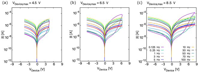
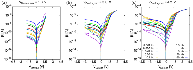
The nonlinearity in memristive devices undergoes significant changes with variations in frequency; therefore, understanding the frequency-dependent behavior of such devices is crucial. For this, different I-V curves of both devices are plotted in Fig. 4 for a sinusoidal input voltage of different amplitudes and frequencies. The following observations can be drawn from the three plots:
(a) For a constant frequency and an increasing maximum device voltage , the hysteresis lobe area increases [31, 13]. This is because the device’s internal state, measured based on the position of oxygen vacancies in BFO and oxygen ions in DBMD, undergoes greater changes at higher voltages. As the voltage increases (decreases), the charged particles experience a greater (lesser) force, resulting in their drift toward the respective interfaces. This leads to an increase (decrease) in current and the difference between the low and high resistance states. However, this argument holds true only for the lower frequency range, a common feature observed in most memristive devices.
(b) For a constant , as the frequency increases, the hysteresis loop area decreases [31, 13]. This phenomenon occurs because the vacancies lack time to jump to a different lattice position and become confined in the same potential well. At lower frequencies, the slower response of the device allows more time for resistive switching mechanisms to manifest, resulting in a larger hysteresis area. As the frequency exceeds 10 Hz for BFO and 1 Hz for DBMD, the I-V curves begin to exhibit behavior similar to that of a normal resistor. Moreover, the change in hysteresis area with frequency in memristive devices can be attributed to the dynamic interplay of capacitive and resistive effects. As the frequency increases, the capacitive reactance decreases, the inductive reactance increases, and vice versa. The impedance equation illustrates that capacitive and inductive reactances balance at certain frequencies, approaching a more resistive behavior. As a result, the capacitive current decreases while the inductive current increases rapidly. The behavior of memristive circuits changes from non-linear to more or less linear resistor-like behavior as the operational frequency varies due to the varying contribution of resistive, capacitive, and inertia effects.
(c) The presence of different effects in these devices have a substantial impact on the zero-crossing current in memristive devices when the frequency of the applied voltage changes. Fig.4 shows that the crossing points move further from the origin as the frequency increases [9], and this effect becomes more pronounced with increasing voltage. As frequency increases and capacitance increases, the battery effect in a circuit becomes more pronounced. The battery effect, commonly linked to the existence of capacitive components, is characterized by the storage and release of charges even when there is no external voltage source. The increased capacitance with frequency is accompanied by a decrease in capacitive reactance, which improves the capacity to store charges. This increased capacitance leads to a more pronounced battery-like effect, where the capacitive component functions as a virtual battery, storing charges and impacting the circuit’s overall behavior. As a result, the increased capacitance with frequency contributes to an enhanced battery effect in the system, moving the crossing point further away from the origin. Moreover, the inertia effects also contribute to the shift in the crossing points. This has been explained in detail by Yarragolla et al[7]. For a frequency of 30 Hz, the change in current is almost linear, and the non-zero crossing disappears.
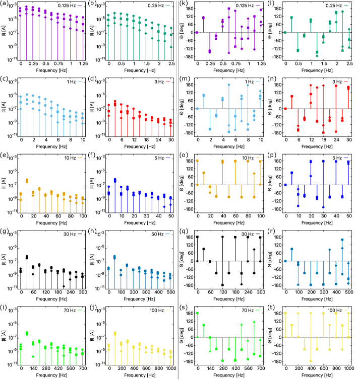
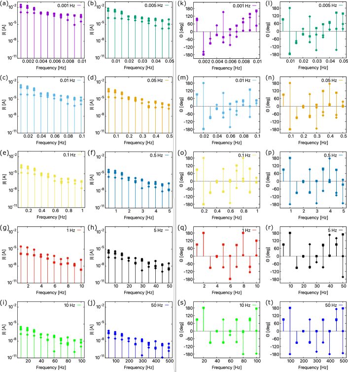
To evaluate the presence of harmonics, we present the frequency spectra of the BFO and DBMD devices in Fig. 6 and Fig. 7, respectively, corresponding to the I-V curves shown in Fig. 4 and Fig. 5. Both devices exhibit a consistent pattern in their amplitude spectra. In Fig. 6(a)-(j) and Fig. 7(a)-(j), as the frequency increases, the hysteresis effects decrease, resulting in a gradual reduction in spikes at lower frequencies. The observed trend indicates a decrease in the dominance of harmonic components in the signal. This phenomenon can be explained by the fact that the impedance of circuit elements, such as resistive, capacitive, and inertial components, exhibits less variation or better balance at lower frequencies. At higher frequencies, spikes show random fluctuations, suggesting the absence of a strong resonance or frequency component. Resonance and harmonics refer to specific frequencies or modes at which the device exhibits heightened responses. These phenomena are often associated with the stochastic non-linear behavior inherent in memristive systems.
As the frequency increases, non-linearities in the circuit, particularly in memristive devices, become more pronounced. Memristors exhibit non-linear resistive switching behavior, which can introduce asymmetrical distortions that favor odd harmonics or cause variations in the amplitudes of both odd and even harmonics. It is important to note that although we observe a somewhat similar trend in the frequency spectra of BFO and DBMD, the non-linearity is less pronounced in DBMD compared to BFO. This discrepancy may have resulted from various factors, such as different geometry considerations. DBMD has a length of only 2.5 nm, and its capacitance is almost two orders of magnitude lower than that of BFO.
The phase plot of frequency spectra of BFO and DBMD are shown in Fig. 6(k)-(t) and Fig. 7(k)-(t), respectively. At low frequencies, the system interacts with complex impedance, which includes resistive, capacitive, and inertia effects, leading to varied phase shifts. The presence of multiple frequency components further complicates the scenario, contributing to seemingly random shifts. The observed phenomenon can be attributed to the system’s response to frequency components. It is important to note that the observed shifts are not random, but rather a result of the system’s interaction with the aforementioned factors. Non-linearities, especially in memristive devices, introduce unpredictability in phase shifts at low frequencies, exhibiting asymmetries. However, at higher frequencies, the shifts stabilize with specific values for even and odd harmonics. As frequencies increase, the stabilization in phase shifts is not driven by resonance but rather linked to the dominance of specific harmonics. This dominance results in stabilized phase shifts for even (odd) harmonics at 180 degrees and odd (even) harmonics at 90 degrees for BFO (DBMD). The intricate combination of device-specific characteristics, non-linear effects, impedance dynamics, and material factors contributes to the distinct phase shift patterns observed in the two memristive devices. The asymmetry in the behavior of even and odd harmonics reflects the nuanced and unique nature of each device’s response to varying frequencies and signal components. Therefore, from these observations, we believe phase plots can serve as unique fingerprints for identifying memristive devices.
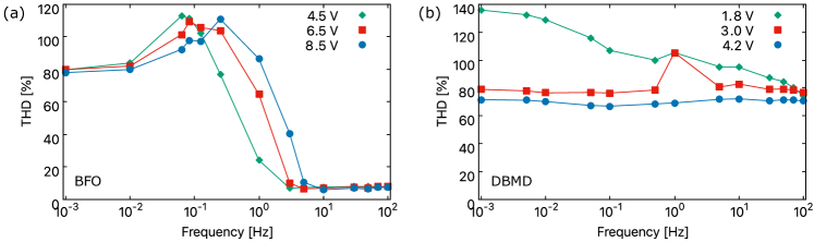
Furthermore, by subjecting memristive devices to a known input signal and analyzing the resulting output signal, one can calculate the total harmonic distortion (THD) as a measure of the distortion introduced by harmonics. Specific THD signatures based on the inherent nonlinear characteristics of different memristive devices or materials can provide a unique identifier. Variations in THD values can indicate differences in the structural or material properties of the memristive device, which contribute to its unique fingerprint. Using THD as a unique identifier for memristive devices enhances identification by introducing greater specificity and complexity to complement other characterization methods, such as current-voltage characteristics and frequency spectrum analysis.
At lower frequencies, the interaction of complex impedance and low-frequency components gradually reduces harmonics, resulting in higher THD as observed in both BFO and DBMD in Fig. 8. On the other hand, higher frequencies exhibit frequency-dependent impedance dynamics, reduced non-linear effects, and a balanced interplay between capacitive and inductive elements, resulting in a cleaner signal with lower THD. As previously stated, reasons such as (a) the device exhibits more resistive current than capacitive current at low frequencies and vice versa at high frequencies due to capacitive reactance, (b) the analogy of inertia effects with kinetic inductance suggests increased inductive reactance at higher frequencies and (c) the cancellation of different effects, result in a more linear device behavior and significantly reduces THD.
From the above discussion, we believe the frequency spectrum of memristive devices provides a unique identifier analogous to the well-established current-voltage characteristics crucial for device characterization and identification. Memristive devices, known for their singular electrical behavior, undergo resistance state changes by applying voltage or current. The device is subjected to alternating current (AC) signals of diverse frequencies to explore its frequency response, which describes how electrical properties change across input frequencies. This behavior is a useful tool for analysis and utilization. Memristive devices or materials exhibit distinct frequency responses, enabling their identification and characterization. Similar to the I-V curves, the frequency spectrum functions as a distinctive identifier, where discrepancies denote material or structural distinctions. In addition, monitoring the frequency response provides an immediate understanding of the status of the memristive device, as variations in the spectrum indicate shifts in resistance states. This active monitoring feature augments the comprehension of memristive devices. Engineers can use the frequency-dependent behavior to optimize device performance, particularly in applications such as neuromorphic computing or resistive switching memory, where nuanced understanding is vital for design and control. therefore, the frequency spectrum is a valuable and versatile tool that provides distinct insights into the behavior and characteristics of memristive devices, complementing the information obtained from traditional I-V curves.
Conclusion
With a special focus on BFO and DBMD devices, this study investigates the nonlinear behavior and non-zero crossing hysteresis of interface-type memristive devices. A physics-based compact model that employs a cloud-in-a-cell scheme is utilized to explore the simultaneous presence of resistive, capacitive, and inductive effects. The physical and chemical processes result in virtual effects in RRAMs. The virtual capacitance arises from numerous factors, including trapping and de-trapping of electrons at the Schottky interface, changes in the density of states across the tunnel barrier capacitance, and electrostatic capacitance of the oxides. Inductive effects occur due to the inertia of the movable defects. The I-V curves demonstrate that capacitive behaviors result in non-zero crossing hysteresis, especially with the BFO device. Conversely, the absence of hysteresis in the DBMD device emphasizes the significance of capacitive effects in determining the behavior of memristive devices, given its significantly lower capacitance. Frequency-dependent change in the I-V curves and shift in the non-zero crossing point with frequency are investigated. The identification of resonances in frequency spectra offers the potential for employing these properties in hardware security and neuromorphic computing applications. A possible solution for implementing PUFs and TRNGs is suggested by the resonance observed in the frequency spectrum of memristive devices. This technique utilizes the characteristic markers provided by the frequency and damping of nonlinear resonances, similar to the utilization of resonant properties in plasma processes. This research significantly enhances the comprehension of nonlinear dynamics in interfacial-type memristive devices, which paves the way for greater utilization of emerging technologies, including secure hardware and neuromorphic computing applications.
Methods
Simulations An in-house model developed using C programming language. The codes developed and implemented are currently research codes that are not yet ready to be used by non-experts.
Data Availability Statement
The datasets used and/or analysed during the current study available from the corresponding author on reasonable request.
References
- [1] Yang, K., Joshua Yang, J., Huang, R. & Yang, Y. Nonlinearity in memristors for neuromorphic dynamic systems. \JournalTitleSmall Science 2, 2100049, DOI: https://doi.org/10.1002/smsc.202100049 (2022). https://onlinelibrary.wiley.com/doi/pdf/10.1002/smsc.202100049.
- [2] Chua, L. Resistance switching memories are memristors. \JournalTitleApplied Physics A 102, 765–783, DOI: 10.1007/s00339-011-6264-9 (2011).
- [3] Strukov, D. B., Snider, G. S., Stewart, D. R. & Williams, R. S. The missing memristor found. \JournalTitleNature 453, 80–83, DOI: 10.1038/nature06932 (2008).
- [4] Ielmini, D. & Waser, R. Resistive Switching: From Fundamentals of Nanoionic Redox Processes to Memristive Device Applications (John Wiley & Sons, Ltd, 2016).
- [5] Chua, L. Everything You Wish to Know About Memristors but Are Afraid to Ask, 89–157 (Springer International Publishing, Cham, 2019).
- [6] Waser, R. & Aono, M. Nanoionics-based resistive switching memories. \JournalTitleNature Materials 6, 833–840, DOI: 10.1038/nmat2023 (2007).
- [7] Yarragolla, S., Hemke, T., Trieschmann, J. & Mussenbrock, T. Non-zero crossing current-voltage characteristics of interface-type resistive switching devices, DOI: https://doi.org/10.48550/arXiv.2401.14507 (2024). ArXiv:2401.14507 [cond-mat.mes-hall].
- [8] Yarragolla, S., Hemke, T., Trieschmann, J. & Mussenbrock, T. Coexistence of resistive capacitive and virtual inductive effects in memristive devices, DOI: https://doi.org/10.48550/arXiv.2401.16057 (2024). ArXiv:2401.16057 [cond-mat.mes-hall].
- [9] Qingjiang, L. et al. Memory impedance in tio2 based metal-insulator-metal devices. \JournalTitleScientific Reports 4, 4522, DOI: 10.1038/srep04522 (2014).
- [10] Setoudeh, F., Dezhdar, M. M. & Najafi, M. Nonlinear analysis and chaos synchronization of a memristive-based chaotic system using adaptive control technique in noisy environments. \JournalTitleChaos, Solitons & Fractals 164, 112710, DOI: https://doi.org/10.1016/j.chaos.2022.112710 (2022).
- [11] Rajendran, S. & Rehman, M. Security of Internet of Things Nodes: Challenges, Attacks, and Countermeasures (Chapman and Hall/CRC,Taylor and Francis Group,, 2021).
- [12] Du, N., Schmidt, H. & Polian, I. Low-power emerging memristive designs towards secure hardware systems for applications in internet of things. \JournalTitleNano Materials Science 3, 186–204, DOI: https://doi.org/10.1016/j.nanoms.2021.01.001 (2021). Nano Energy Materials and Devices for Miniaturized Electronics and Smart Systems.
- [13] Yarragolla, S. et al. Stochastic behavior of an interface-based memristive device. \JournalTitleJournal of Applied Physics 131, 134304, DOI: 10.1063/5.0084085 (2022).
- [14] Yarragolla, S. et al. Physics inspired compact modelling of bifeo3 based memristors. \JournalTitleScientific Reports 12, 20490, DOI: 10.1038/s41598-022-24439-4 (2022).
- [15] Yarragolla, S., Hemke, T. & Mussenbrock, T. A generic compact and stochastic model for non-filamentary analog resistive switching devices. In 2023 12th International Conference on Modern Circuits and Systems Technologies (MOCAST), 1–4, DOI: 10.1109/MOCAST57943.2023.10176574 (2023).
- [16] Du, N. et al. Field-driven hopping transport of oxygen vacancies in memristive oxide switches with interface-mediated resistive switching. \JournalTitlePhys. Rev. Applied 10, 054025, DOI: 10.1103/PhysRevApplied.10.054025 (2018).
- [17] Hansen, M. et al. A double barrier memristive device. \JournalTitleScientific Reports 5, 13753, DOI: 10.1038/srep13753 (2015).
- [18] Laux, S. E. On particle-mesh coupling in monte carlo semiconductor device simulation. \JournalTitleIEEE Transactions on Computer-Aided Design of Integrated Circuits and Systems 15, 1266–1277, DOI: 10.1109/43.541446 (1996).
- [19] Bruce, P. G. Solid State Electrochemistry. Chemistry of Solid State Materials (Cambridge University Press, 1994).
- [20] Meyer, R. et al. Oxide dual-layer memory element for scalable non-volatile cross-point memory technology. In Proceedings - 9th Annual Non-Volatile Memory Technology Symposium, NVMTS, DOI: 10.1109/NVMT.2008.4731194 (2008).
- [21] Sze, S. M. & Ng, K. K. Physics of Semiconductor Devices (John Wiley & Sons Ltd,, 2007).
- [22] Simmons, J. G. Generalized formula for the electric tunnel effect between similar electrodes separated by a thin insulating film. \JournalTitleJournal of Applied Physics 34, 1793–1803, DOI: 10.1063/1.1702682 (1963).
- [23] Grundmann, M. The Physics of Semiconductors: An Introduction Including Nanophysics and Applications. Graduate Texts in Physics (Springer International Publishing, 2015).
- [24] Datta, S. Quantum Transport: Atom to Transistor (Cambridge University Press, 2005).
- [25] Yan, Z. B. & Liu, J.-M. Coexistence of high performance resistance and capacitance memory based on multilayered metal-oxide structures. \JournalTitleScientific Reports 3, 2482, DOI: 10.1038/srep02482 (2013).
- [26] John, D. L., Castro, L. C. & Pulfrey, D. L. Quantum capacitance in nanoscale device modeling. \JournalTitleJournal of Applied Physics 96, 5180–5184, DOI: 10.1063/1.1803614 (2004). https://pubs.aip.org/aip/jap/article-pdf/96/9/5180/13944676/5180_1_online.pdf.
- [27] Di Ventra, M., Pershin, Y. V. & Chua, L. O. Circuit elements with memory: Memristors, memcapacitors, and meminductors. \JournalTitleProceedings of the IEEE 97, 1717–1724, DOI: 10.1109/JPROC.2009.2021077 (2009).
- [28] Biolek, D., Biolek, Z. & Biolková, V. PSPICE modeling of meminductor. \JournalTitleAnalog Integrated Circuits and Signal Processing 66, 129–137, DOI: 10.1007/s10470-010-9505-5 (2011).
- [29] Marquardt, R. et al. Impedance spectroscopy on hafnium oxide-based memristive devices. \JournalTitleAdvanced Electronic Materials 9, 2201227, DOI: https://doi.org/10.1002/aelm.202201227 (2023). https://onlinelibrary.wiley.com/doi/pdf/10.1002/aelm.202201227.
- [30] Bisquert, J. & Guerrero, A. Chemical inductor. \JournalTitleJournal of the American Chemical Society 144, 5996–6009, DOI: 10.1021/jacs.2c00777 (2022). PMID: 35316040, https://doi.org/10.1021/jacs.2c00777.
- [31] Maestro-Izquierdo, M., Gonzalez, M. B., Campabadal, F., Suñé, J. & Miranda, E. A new perspective towards the understanding of the frequency-dependent behavior of memristive devices. \JournalTitleIEEE Electron Device Letters 42, 565–568, DOI: 10.1109/LED.2021.3063239 (2021).
Acknowledgements
Funded by the Deutsche Forschungsgemeinschaft (DFG, German Research Foundation) - Project-ID 434434223- SFB 1461 and Project-ID 439700144- Research Grant MU 2332/10-1 in the frame of Priority Program SPP 2253.
Author contributions statement
S.Y. prepared the data sets, implemented the methodology, conducted the simulations, analysed the results, and prepared the first draft of the manuscript. T.M. and J.T. conceived and directed the conceptual ideas of the work. S. Y., T.H. and T.M. developed the methodological concept for memristor modeling. T.M. acquired the funding and administered the project. All authors contributed with interpreting and discussing the results as well as manuscript writing and revision.
Competing interests
The authors declare no competing interests.