Ab initio study of subsurface diffusion of Cu on the H-passivated Si(001) surface
Abstract
In this paper we use density-functional theory calculations to analyze both the stability and diffusion of Cu adatoms near and on the H-passivated Si(001) surface. Two different Cu sources are considered: depositing Cu from vacuum, and contaminating Cu outdiffusing from bulk Si. Deposited Cu from vacuum quickly moves subsurface to an interstitial site in the third Si layer (T2). Once there, Cu adatoms enter a subsurface zigzag migration route between T2 and another subsurface site, T2→HSL→T2, along the dimer row direction. Contaminating Cu outdiffusing from bulk is found to be a fast diffuser along both parallel and perpendicular directions to the dimer row when far from the surface. It is attracted to the layers close to the surface and becomes trapped at an interstitial site located at the sixth Si layer (T3). As the outdiffusing Cu atoms get closer to the surface, a channeling zigzag diffusion along the dimer row direction, similar to that one followed by deposited Cu from vacuum, is favoured over diffusion along the perpendicular direction. These results are consistent with previous experimental work done on similar systems and will motivate further experiments on the interesting interaction between Cu and Si surfaces.
I Introduction
A clear theoretical understanding of the defects which affect the performance of silicon-based complementary metaloxide semiconductor devices is still far from complete and would be of enormous benefit. Copper is a highly detrimental and very common contaminant in device manufacturing Foster2007 especially since its introduction as the metal for interconnects. It is an extremely fast diffuser in Si, even at room temperature Istratov1998 and forms silicides which degrade device characteristics. When adsorbed on clean Si(001), Cu forms a distinctive three-lobed linear feature perpendicular to the dimer rows which orders to form a c(8x8) reconstruction at high coverages Liu2000 . On addition of hydrogen to a Cu-dosed surface, the feature sizes and appearance change, suggesting that the Cu may be subsurface Baker2005 , though the structure of these features is still unknown. The adsorption of hydrogen onto Si(001) follows various stages Boland1993 : very low coverages lead to single hydrogen atoms adsorbed on one side of a dimer, giving a hemihydride Radny2007 ; however, when the coverage goes beyond more than about 0.1 ML, these single hydrogens rapidly pair up to form saturated dimers Boland1991 with one hydrogen for each dangling bond; adsorption of a full monolayer leads to the saturated, monohydride surface. This surface, notated H:Si(001), is generally very well ordered and unreactive; it can be used as a mask when creating features such as dangling-bond wires Bowler2004 or for overgrowth of systems such as the Bi nanolines which self-assemble on Si(001) Owen2006 . While the overgrowth of Bi lines with the noble metals such as Ag and Au has been considered, Cu has not been used, presumably because of its tendency to act as a contaminant. Here, we present a density-functional theory (DFT) study of the behaviour of Cu at and below H:Si(001), considering both the low-energy structures formed and the diffusion barriers. In a related paper we model the interaction of Cu with Bi nanolines on H:Si(001). Our purpose is to understand the behaviour of this important metal at the H:Si(001) surface and possible mechanisms for decoration of the surface and Bi nanolines. After detailing our methods, we consider first the stable sites for Cu near H:Si(001), and then diffusion barriers for Cu starting on the surface and coming from the bulk, after which we conclude.
II Theoretical and Computational Background
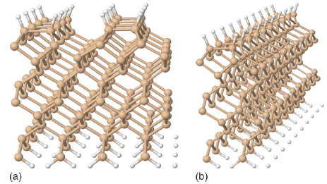
We have used a plane-wave implementation of DFT (Refs. Hohenberg1964 and Kohn1965 ) within the local density approximationCeperley1980 ; Perdew1981 ; Perdew1992 . All calculations have been performed with the Vienna ab initio simulation package (VASP) (Refs. Kresse1993 and Kresse1996 ). Ultrasoft pseudopotentials (Ref. 18) are used for all the elements considered: Cu, Si, and H. We use an energy cutoff of 233.781 eV for the plane waves (which converges energy differences). To understand the interaction of Cu with the H:Si(001) surface, we use a slab with two dimer rows, each containing four dimers (giving an area of 15.36 Å x 15.36 Å) and with ten layers. This guarantees that the Cu atoms in different cells will not interact. For related studies involving the interaction of Cu with Bi nanolines, we must use a computational cell with a rather different shape: the nanolines require a cell ten-dimers long and ten-layers deep, which practically restricts us to a unit-cell one-dimer row wide for most calculations. We have therefore repeated our calculations in a cell of this size to check on the effect of cell size and possible interactions between Cu atoms in neighbouring cells. Both cells are illustrated in Fig. 1. For both cells, the bottom two layers are fixed into their bulk positions and terminated with two H atoms each to simulate bulk conditions, whereas the surface dimers (pairs of atoms bonded to each other with one dangling bond) contained within the slab are covered with a monohydride surface. The square cell contains 16 Si atoms per layer and 48 H atoms in total, giving 208 atoms while the longer thin cell contains 20 Si atoms per layer and 60 H atoms in total, giving 260 atoms. We use a Monkhorst-Pack Monkhorst1976 mesh of 4x4x1 to sample the Brillouin Zone for the square cell, and 4x2x1 for the long, thin cell; both of these give energy-difference convergence. Calculations of barrier heights used the nudged elastic band method Henkelman2000 with a single image (which is equivalent to the dimer method Henkelman1999 with very close images or the force inversion method Tateyama1996 and gives excellent convergence of energy-barrier heights). For a number of the migration routes considered, we found that the Si-Si distances were sufficiently small that the passage of Cu-caused significant rearrangements of the lattice and extremely large energy barriers. We label these routes as “n/a” in Sec. IV.
III Stable sites for Cu near H:Si(001)
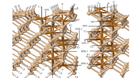
We consider first the binding energies (BEs) of Cu at different possible sites below and at the H:Si(001) surface. The optimized geometries of the most energetically favoured positions are then studied in detail. The diffusion of Cu on and below the H-passivated Si(001) surface is described in Sec. IV, where different migration routes with their corresponding energy barriers will be examined. All the candidate sites are illustrated in Fig. 2 with binding energies given in Table I. We have selected different adsorption sites both on the surface and below the surface. On the surface we consider: the cave site C(-4.41 eV), on the side of a dimer at the trench between dimer rows; the pedestal site P(-4.05 eV) between two adjacent dimers along the dimer row; and the site A(-3.96 eV) close to the Si-H bond of one of the dimers. Below the surface we consider three tetrahedral sites: T4(-4.49 eV), T3(-4.65 eV), and T2(-4.60 eV); and four other sites inside the hexagonal cages: HSL(-4.60 eV), HSL2(-4.62 eV), HSL3(-4.53 eV), and HSL4(-4.36 eV). An additional adsorption site below the dimers, BD(-3.81 eV) is also considered. These energies are summarised in Table I. The T2 and T3 sites show lower binding energies than T4, which indicates that, despite the well-known property of Cu as a fast diffuser inside bulk Si, it will tend to be adsorbed close to the top layers of the H-passivated Si(001) surface; we explore the attraction mechanism of Cu to defects elsewhere. Similarly, HSL2 and HSL3 show lower BEs than HSL4. However, HSL has a BE slightly higher than HSL2, as does T2 with respect to T3. This indicates that despite a clear tendency for Cu to be adsorbed close to the surface, it does not go to the top Si layers. It is also noteworthy that tetrahedral positions inside bulk Si(T5,T6, …) show the same BE as T4 so that the energies of these sites are not affected by the constrained bottom layers. The most energetically favoured sites (T3, HSL2, T2, and HSL in descending energy) are located between the third and the sixth layers. The next sites in energy are HSL3, T4, C, and HSL4, whereas the rest of the sites show sufficiently poor energies to be unimportant and are not considered further. The large gap in energy which opens between the C and P sites is a key indicator. The pedestal P site and its close A site already show energies 0.60 and 0.69 eV higher than T3. Below the dimers, BD, is even worse, with an energy 0.83 eV higher and, finally, the B site presents a really poor energy due to the strong Si-Si bond of the dimers.
| Adsorp. site | (eV) | Binding energy (eV) |
|---|---|---|
| T3 | 0 | -4.65 |
| HSL2 | 0.03 | -4.62 |
| T2 | 0.05 | -4.60 |
| HSL | 0.05 | -4.60 |
| HSL3 | 0.12 | -4.53 |
| T4 | 0.16 | -4.49 |
| C | 0.24 | -4.41 |
| HSL4 | 0.29 | -4.36 |
| P | 0.60 | -4.05 |
| A | 0.69 | -3.96 |
| BD | 0.83 | -3.82 |
IV Cu diffusion near H-passivated Si(001)
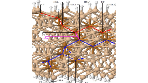
In this section, we investigate the energy barriers for migration routes for Cu diffusion. As mentioned above, we will consider two different Cu sources: Cu deposited from vacuum and Cu outdiffusing from bulk Si. All the migration routes considered are shown in Figure 3 (Cu deposited from vacuum) and Fig. 4 (contaminating Cu inside bulk Si).
IV.1 Depositing Cu from vacuum
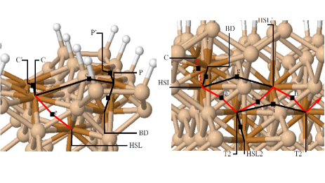
When Cu is deposited from vacuum onto a H-passivated Si(001) surface it will first reach one of the adsorption sites considered above on the surface: C(-4.41 eV), P(-4.05 eV), and A(-3.96 eV), with C being the most feasible site as its BE is the lowest by far. We will show how adatoms adsorbed at A and P will move to C. These are illustrated in Fig. 3(a). A Cu adatom adsorbed at the A site would easily move to P through a barrier of =0.20 eV. Bringing one Cu adatom between two consecutive P sites along the dimer row direction, P and P’ requires a high energy barrier, Eb=0.71 eV. The P→BD route crosses a trapezium where the very short Si-Si bonds (2.43, 2.51, and 3.80 nm) do not give enough space for the Cu adatom to migrate through; this is the first example of a migration route labelled “n/a” and described in Sec. II. In addition, the P→C route, which brings the adtom to a site whose BE is 0.36 eV better, presents a reasonable =0.44 eV, so that this becomes the most likely route. For the adatom at C, which is the position most likely to be reached by deposited Cu adatoms in a first instance, moving to P is unlikely as C→P route presents a very high =0.80 eV. On the other hand, a possible migration route C→C’ (with no energy gain) along the dimer trench shows a relatively high =0.45 eV, compared to the C→HSL route, with a very low =0.06 eV to a site whose BE is 0.19 eV lower. This indicates essentially free movement of adatoms from C to HSL. It is interesting to note that previous studies (Ref. 24) show that Ag adatoms on a H-passivated Si(001) surface do migrate through the dimer trench, C→C’→C; this is likely related to the relative sizes of Cu and Ag. Let us consider now the different migrating posibilities of Cu adatoms based at HSL (Fig. 3(b)). They could diffuse towards either BD, C, or T2 sites, since bringing an adatom from HSL to HSL’ directly through the route between the two Si atoms is not feasible as the Si-Si bond there is so small. The HSL→BD route has a very high =0.83 eV, whereas bringing the adatom to T2 (a site with the same BE), HSL→T2, requires only 0.17 eV. Finally, returning to C (whose BE is 0.19 higher), HSL→C shows an energy barrier =0.19 eV. Therefore, a large number of adatoms will move to T2 directly. On the other hand while a considerable fraction of Cu atoms could move to C, they will return to HSL (with Eb=0.06 eV), and, eventually, diffuse towards T2. Possible migration routes for adatoms at T2 are displayed also in Fig. 3(b). A direct route from T2 to T2’ would again find the problem of small Si-Si distances. So the possibilities for a Cu atom at T2 are either to return to the hexagonal site HSL’, a site with the same BE, through an energy barrier =0.17 eV, or migrating to the hexagonal site HSL2, with a BE only 0.02 eV lower, through a barrier almost two times higher, =0.28 eV. As BEs of HSL’ and HSL2 differ only 0.02 eV, it is the much lower energy barrier of the T2→HSL’ route which becomes a key factor and will enhance this route as the most feasible migration route. From HSL’, as we have seen above when dealing with the migration routes from HSL, Cu adatoms will move towards T2’. Thus, once adatoms reach T2, they enter a subsurface zigzag migration route through the sites T2 and HSL, diffusing along the Si dimer row direction, between the fourth and the fifth Si layers. Finally a possible alternative subsurface migration route along the direction perpendicular to the dimer row, T2→HSL2→T2p (where T2p means the next consecutive T2 site along the direction perpendicular to the dimer row), is much less likely due to the higher energy barriers, 0.28 and 0.30 eV, respectively.
IV.2 Contaminating Cu inside bulk Si
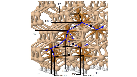
As we have noted above, Cu is known to be a fast diffuser inside bulk Si and to contaminate Si samples easily. Therefore, contaminating Cu diffusing through bulk Si might well be an alternative source of Cu adatoms at the surface. We have already seen that Cu shows a clear tendency to be adsorbed close to the surface. In what follows, we investigate the possible migration routes from bulk to the adsorption sites near the H-passivated Si(001) surface. We choose HSL4 as our starting point. We note that this is verstudy of subsurface diffusiony close to the constrained, bulklike layers, but have confirmed that the diffusion barriers away from this site are equal to the bulk diffusion barrier (of 0.25 eV), and conclude that the constraint has only a small effect on diffusion away from the HSL4 site. It is clear that the HSL4→HSL4’ and HSL4→HSL4p (here HSL4’ means the next consecutive HSL4 site along the dimer row direction, whereas HSL4p means the next consecutive HSL4 site along the direction perpendicular to the dimer row) direct route is not feasible due again to the very small Si-Si bond along this route. On the other hand, a HSL4→T4 route has a small barrier =0.15 eV, so that Cu moves towards T4, with a BE 0.12 eV lower than HSL4. Once at T4, Cu could migrate to either HSL4 or HSL3. The T4→HSL3 is the most feasible route, as the barrier is relatively small (=0.20 eV) and HSL3 has a BE 0.04 eV lower than T4. However, the T4→HSL4p route presents a =0.27 eV to a site 0.12 eV higher in BE, which makes possible an alternative zigzag subsurface migration route T4→HSL4p→T4p along the direction perpendicular to the dimer row. From HSL3, we consider possible migrations to T4’ and T3. Again, although more Cu adatoms will follow the HSL3→T3 route, moving to a site whose BE is 0.12 eV lower through a smaller barrier =0.18 eV, some other adatoms might move towards T4’, with a BE 0.04 eV higher, through a slightly higher barrier =0.25 eV. Thus, despite the tendency of Cu adatoms at HSL4 and T4 to move towards T3, alternative zigzag migration routes along both parallel and perpendicular directions to the dimer row emerge, with the parallel route being more likely. This alternative migration routes confirm the idea of fast diffusing Cu. Once at T3 we check again three possibilities: moving upwards through HSL2 up to T2, or entering a zigzag subsurface migration routes either along the dimer row direction, T3→HSL2→T3’, or perpendicular to the dimer row direction, T3→HSL3p→T3p. The energy barriers are (T3→HSL3)=0.30 eV, (T3→HSL2)0.23 eV, (HSL2→T3)=0.20 eV, and (HSL2→T2)=0.30 eV, whereas relative to the BE of the most energetically favoured adsorption site T3, the BEs of HSL3, HSL2, and T2 are 0.12, 0.03, and 0.05 eV higher. Therefore, Cu adatoms are most likely to enter the migration route along the dimer row direction, T3→HSL2→T3’. The perpendicular migration route is also possible but less likely to happen. Note that the fraction of Cu adatoms moving along the dimer row direction has been increased compared to that one at T4 (where although more adatoms diffused through the dimer row directions a relative high fraction of Cu could possible migrate along the perpendicular direction). Finally, the large energy barrier between HSL2 and T2, =0.30 eV, makes the movement to T2, and entering the T2→HSL→T2’ migration route followed by deposited Cu from vacuum, more unlikely although kinetically possible. Similarly, although most of deposited Cu from vacuum follow the T2→HSL→T2’ migration route, a small fraction of adatoms could migrate from T2 to HSL2 and enter the T3→HSL2→T3’ route. Nevertheless, a vast majority of deposited Cu would migrate along the dimer row direction. Therefore, this large barrier prevents a large mixing between deposited Cu from vacuum and contaminating Cu outdiffusing from bulk Si. We can conclude that both Cu sources diffuse through different migration routes, although some mixing can be expected. To conclude, it is noteworthy that, in spite of multiple diffusion directions in the botton layers, as we go up, closer to the surface, Cu diffusion gets more channeled along the dimer row direction. In Fig. 5 we summarize the lowest-energy-migration routes for Cu deposited from vacuum and contaminating Cu inside bulk Si. Deposited Cu from vacuum follow the route (P→)C→HSL, with =0.06 eV, to enter the zigzag migration route T2→HSL→T2’ with =0.17 eV. Contaminating Cu outdiffusing from bulk can diffuse along different directions, specially when located in the bottom Si layers. However, we display the most feasible migration route HSL4→T4→HSL3→T3 to T3, where adatoms enter a zigzag migration route T3→HSL2→T3’. Energy barriers are (HSL4→T4)=0.15 eV, (T4→HSL3)=0.20 eV, and (HSL3→T3)=0.18 eV, and for the zigzag migration route (T3→HSL2) =0.23 eV and (HSL2→T3)=0.20 eV (Table II).
| Saddle point | Binding energy (eV) | Connecting |
|---|---|---|
| a | -3.34 | P, P’ |
| b | n/a | P, BD |
| c | -3.61 | P, C |
| d | -3.96 | C, C’ |
| e | -4.35 | C, HSL |
| f | -3.77 | HSL, BD |
| g | n/a | HSL, HSL’ |
| h | -4.43 | HSL, T2 |
| i | n/a | T2, T2’ |
| j | -4.32 | T2, HSL2 |
| k | -4.42 | T3, HSL2 |
| l | -4.35 | HSL3, T3 |
| m | -4.29 | T4, HSL3 |
| n | n/a | T4, T4’ |
| o | -4.22 | HSL4, T4 |
| p | n/a | HSL4, HSL4’ |
V Results with the one-dimer row slab
Having established the behaviour of copper in isolation, we now consider the second unit cell described in Sec. II and Fig. 1(b), which contains one dimer row with ten Si dimers and ten layers, and will be suitable for calculations on Bi nanolines. Our concern is to investigate the influence of the narrow cell on the Cu energies and barriers.
V.1 Stable sites for Cu near H:Si(001)
In Table III we display the BEs of the adsorption sites,
following the same nomenclature as above. As we see,
T3(-5.06 eV) is again the most favourable adsorption site,
followed by HSL2(-5.04 eV), T2(-5.02 eV), and
HSL(-4.99 eV). Although there is a quantitative change in
the BEs, no qualitative difference is observed when compared
with the results obtained with the first slab. The adsorption
positions are ordered exactly in the same way and
the values of are very similar. When using the onedimer
cell one could think that, due to the periodicity along
the direction perpendicular to the dimer row, interactions between
Cu atoms in the neighbouring cell are not neglected.
The fact that there is no qualitative difference at all between
BEs in cells containing one and two dimer rows, respectively,
indicate that this interaction does not play a significant
role. Nevertheless, in what following we will study the energy
barriers and migration routes followed by Cu within the
one-dimer row slab so that we can compare these results to
those obtained earlier. This should give us a better idea on
the issue.
| Adsorp. site | (eV) | Binding energy (eV) |
|---|---|---|
| T3 | 0 | -5.06 |
| HSL2 | 0.02 | -5.04 |
| T2 | 0.04 | -5.02 |
| HSL | 0.07 | -4.99 |
| HSL3 | 0.10 | -4.96 |
| T4 | 0.20 | -4.86 |
| C | 0.21 | -4.85 |
| HSL4 | 0.24 | -4.82 |
| P | 0.69 | -4.37 |
| A | 0.69 | -4.37 |
| BD | 0.81 | -4.25 |
| B | xx | xx |
V.2 Depositing Cu from vacuum
The adsorption sites considered above on the surface are: C(-4.85 eV), P(-4.37 eV), A(-4.37 eV), and B(-3.36 eV). As binding energy of B is so bad, we neglect this site, and consider only the P (A site is very similar) and C sites. Energy barriers from P(-4.37 eV) to P’ and C(-4.85 eV) are 1.2 and 0.38 eV, respectively, whereas route towards BD(-4.25 eV) is not feasible due to small Si-Si bonds. So that Cu adatoms clearly diffuse to C site, as seen above, though with slightly higher barriers. Energy barriers from C(-4.85 eV) to C’, P(-4.37 eV) and HSL(-4.99 eV) are 0.53, 0.86, and 0.06 eV, in good agreement with results from the other cell. Therefore, adatoms migrate from C to HSL, where possibilities are moving to BD(-4.25 eV), C, and T2(-5.02 eV), through barriers of 0.45, 0.18, and 0.17 eV. Most of the adatoms will move directly to T2, while a smaller fraction could go back to C, from where they will come again to HSL, eventually diffusing to T2. At T2, possibilities are moving to HSL’(-4.99 eV) through a 0.20 eV barrier or to HSL2(-5.04 eV) through a much larger 0.40 eV barrier. It is clear, then, than Cu adatoms follow a P→C→HSL path to enter a zigzag subsurface diffusion route along the dimer row direction HSL→T2→HSL’→T2’. This agrees very well with the migration route calculated with the other slab model.
V.3 Outdiffusing Cu from bulk
In what follows, we investigate the possible migration routes from bulk to the adsorption sites near the H-passivated Si(001) surface. We start from HSL4(-4.82 eV), from where the only possibility is moving to T4(-4.86 eV) through a 0.19 eV barrier. Energy barrier from T4 to HSL4 is 0.25 eV whereas moving to HSL3(-4.96 eV) requires only 0.19 eV. The latter possibility is, then, more feasible, but a zigzag route T4→HSL4p→T4p along the direction perpendicular to the dimer row is also possible; these barriers agree well with the other cell. From HSL3, most adatoms will move to T3(-5.06 eV) through a 0.22 eV barrier but a small fraction of adatoms could move to T4’ through a 0.29 eV barrier. Therefore, despite the tendency of Cu to move from HSL4 and T4 to T3, alternative zigzag migration routes emerge along both the parallel and perpendicular directions to the dimer row, just as it happened when using the former slab model. At T3 three possibilities emerge: moving upwards through HSL2(-5.04 eV) to T2(-5.02 eV), or enter the zigzag migration routes either along the dimer row direction T3→HSL2→T3’, or along the perpendicular T3→HSL3p→T3p. The energy barriers are (T3→HSL3)=0.32 eV, (T3→HSL2)=0.24 eV, (HSL2→T3)=0.22 eV, and (HSL2→T2)=0.42 eV, whereas relative to the BE of the most energetically favoured adsorption site T3, the BEs of HSL3, HSL2 and T2 are 0.10, 0.02, and 0.04 eV higher. Therefore, Cu adatoms are most likely to enter the migration route along the dimer row direction, T3→HSL2→T3’. The perpendicular migration route is also possible but less likely to happen. Note that the fraction of Cu adatoms moving along the dimer row direction has been increased compared to that one at T4 (where although more adatoms diffused through the dimer row directions a relative high fraction of Cu could possible migrate along the perpendicular direction). Again, this facts were also observed in the previous calculations with the other slab. Finally, the large energy barrier between HSL2 and T2, =0.42 eV, makes the movement to T2, and entering the T2→HSL→T2’ migration route followed by deposited Cu from vacuum, unlikely although kinetically possible. Therefore, this large barrier prevents a mixing between deposited Cu from vacuum and contaminating Cu outdiffusing from bulk Si. This barrier also arises when calculating with a twodimer rows slab model, although it is slightly smaller. To summarize: no qualitative difference is observed when considering slabs containing one and two dimer rows so that we can conclude considering one-dimer row slab is enough as the interaction between Cu adatoms situated in neighboring cells is not significant. Adsorption positions are sorted in the same way in terms of BE while the most likely migration routes are identical. Some small changes have been identified, including a shift in the BE but not in the BE difference . Also, when considering the one-dimer row slab, a clear gap opens between the migration routes followed by Cu deposited from vacuum and Cu coming from inner layers. Such an energy gap also emerges in the case of the two dimer rows slab, although it is smaller and allows a certain mixing between Cu coming from the two different sources.
VI Conclusions
In this paper we have investigated the adsorption and diffusion of Cu adatoms on the H-passivated Si(001) surface. We have seen that both the tetrahedral sites T3 and T2, and the hexagonal sites HSL2 and HSL emerge as the lowest adsorption energy sites, so that despite the behaviour of Cu as a fast diffuser inside bulk Si, it tends to be adsorbed close to the surface. In addition, Cu diffusion for two different sources of adatoms has been examined. Deposited Cu from vacuum follow the route (P→)C→HSL, with =0.06 eV, to enter the zigzag migration route T2→HSL→T2’ with =0.17 eV. Although contaminating Cu outdiffusing from bulk can diffuse along different directions, the most feasible migration route is HSL4→T4→HSL3→T3 to T3, where adatoms enter a zigzag migration route T3→HSL2→T3’. Energy barriers are (HSL4→T4)=0.15 eV, (T4→HSL3)=0.20 eV, and (HSL3→T3)=0.18 eV, and for the zigzag migration route (T3→HSL2) =0.23 eV and (HSL2→T3)=0.20 eV. Therefore, both Cu starting on the surface (after deposition from vacuum) and Cu assumed to be contaminating bulk Si diffuse along the dimer row direction through subsurface zigzag migration routes. Although contaminating Cu adatoms might diffuse also along the direction perpendicular to the dimer row when located in the inner layers, a progressive channeling along the dimer row direction emerges as adatoms migrate upward to the surface.
VII Acknowledgments
We acknowledge useful discussions with Flemming Ehlers and James Owen. A. Rodriguez-Prieto. was funded by the Basque Government. D.R. Bowler was funded by the Royal Society. The computational work was performed at the London Centre for Nanotechnology (LCN), UCL.
References
- [1] A. S. Foster et al. . Phys. Rev. B, 76:075315, 2007.
- [2] A. A. Istratov et al. . Phys. Rev. Lett, 81:1243, 1998.
- [3] B. Liu et al. . Surf. Sci., 453:137, 2000.
- [4] L. A. Baker et al. . Phys. Rev. B, 71:153302, 2005.
- [5] J. J. Boland. . Adv. Phys., 42:129, 1993.
- [6] M. W. Radny et al. . Phys. Rev. B, 76:155302, 2007.
- [7] J. J. Boland. . Phys. Rev. Lett., 67:1539, 1991.
- [8] D. R. Bowler. . J. Phys.: Condens. Matter, 16:R721, 2004.
- [9] J. H. G. Owen et al. . J. Matter Sci., 41:4568, 2006.
- [10] P. Hohenberg et al. . Phys. Rev., 136:B864, 1964.
- [11] W. Kohn et al. . Phys. Rev., 140:A1133, 1965.
- [12] D. M. Ceperley et al. . Phys. Rev. Lett., 45:566, 1980.
- [13] J. P. Perdew et al. . Phys. Rev. B, 23:5048, 1981.
- [14] J. P. Perdew et al. . Phys. Rev. B, 45:13244, 1992.
- [15] G. Kresse et al. . Phys. Rev. B, 47:558, 1993.
- [16] G. Kresse et al. . Phys. Rev. B, 54:11169, 1996.
- [17] H. J. Monkhorst et al. . Phys. Rev. B, 13:5188, 1976.
- [18] G. Henkelman et al. . J. Chem. Phys., 113:9978, 2000.
- [19] G. Henkelman et al. . J. Chem. Phys., 111:7010, 1999.
- [20] Y. Tateyama et al. . Phys. Rev. B, 54:14994, 1996.